TC74VHCT244AFT(EL),TC74VHCT244AFW,TC74VHCT240AFT(EL),TC74VHCT240AFW, 规格书,Datasheet 资料
- 格式:pdf
- 大小:215.08 KB
- 文档页数:9

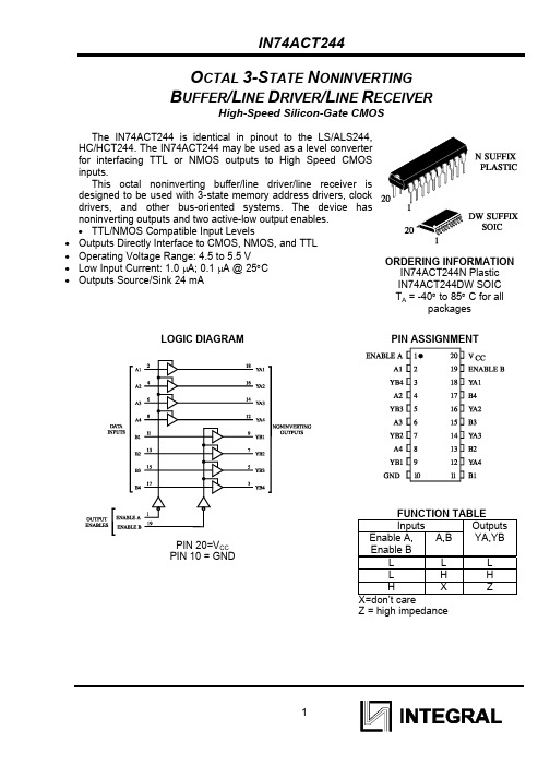
O CTAL 3-S TATE N ONINVERTINGB UFFER/L INE D RIVER/L INE R ECEIVERHigh-Speed Silicon-Gate CMOS The IN74ACT244 is identical in pinout to the LS/ALS244, HC/HCT244. The IN74ACT244 may be used as a level converterfor interfacing TTL or NMOS outputs to High Speed CMOSinputs.designed to be used with 3-state memory address drivers, clocknoninverting outputs and two active-low output enables.•TTL/NMOS Compatible Input Levels•Outputs Directly Interface to CMOS, NMOS, and TTL•Operating Voltage Range: 4.5 to 5.5 V •Low Input Current: 1.0 µA; 0.1 µA @ 25°C •Outputs Source/Sink 24 mAORDERING INFORMATIONIN74ACT244N PlasticIN74ACT244DW SOICT A = -40° to 85° C for allpackagesFUNCTION TABLEInputs Outputs Enable A,Enable BA,B YA,YBL L LL H HH X ZX=don’t careZ = high impedanceLOGIC DIAGRAMPIN 20=V CCPIN 10 = GNDPIN ASSIGNMENTMAXIMUM RATINGS*Symbol Parameter ValueUnit V CC DC Supply Voltage (Referenced to GND) -0.5 to +7.0 VV IN DC Input Voltage (Referenced to GND) -0.5 to V CC +0.5 VV OUT DC Output Voltage (Referenced to GND) -0.5 to V CC +0.5 VI IN DC Input Current, per Pin ±20 mAI OUT DC Output Sink/Source Current, per Pin ±50 mAI CC DC Supply Current, V CC and GND Pins ±50 mAP D Power Dissipation in Still Air, Plastic DIP+ SOIC Package+ 750500mWTstg Storage Temperature -65 to +150 °CT L Lead Temperature, 1 mm from Case for 10Seconds(Plastic DIP or SOIC Package)260 °C*Maximum Ratings are those values beyond which damage to the device may occur.Functional operation should be restricted to the Recommended Operating Conditions.+Derating - Plastic DIP: - 10 mW/°C from 65° to 125°CSOIC Package: - 7 mW/°C from 65° to 125°CRECOMMENDED OPERATING CONDITIONSSymbol Parameter MinMaxUnit V CC DC Supply Voltage (Referenced to GND) 4.5 5.5 VV IN, V OUT DC Input Voltage, Output Voltage (Referenced toGND)0 V CC VT J Junction Temperature (PDIP) 140 °CT A Operating Temperature, All Package Types -40 +85 °CI OH Output Current - High -24 mAI OL Output Current - Low 24 mAt r, t f Input Rise and Fall Time * (except Schmitt Inputs) V CC=4.5 VV CC =5.5 V108.0ns/V* VINfrom 0.8 V to 2.0 VThis device contains protection circuitry to guard against damage due to high static voltages or electric fields. However, precautions must be taken to avoid applications of any voltage higher than maximum rated voltages to this high-impedance circuit. For proper operation, V IN and V OUT should be constrained to the range GND≤(V IN or V OUT)≤V CC.Unused inputs must always be tied to an appropriate logic voltage level (e.g., either GND or V CC). Unused outputs must be left open.DC ELECTRICAL CHARACTERISTICS (Voltages Referenced to GND)V CC Guaranteed LimitsSymbol Parameter Test Conditions V 25 °C -40°C to85°CUnit V IH Minimum High-Level Input VoltageV OUT = V CC -0.1 V 4.5 5.5 2.0 2.0 2.0 2.0 VV IL Maximum Low -Level Input VoltageV OUT =0.1 V 4.5 5.5 0.8 0.8 0.8 0.8 VV OH Minimum High-Level Output VoltageI OUT ≤ -50 µA 4.5 5.5 4.4 5.4 4.4 5.4 V*V IN =V IHI OH =-24 mAI OH =-24 mA4.55.5 3.86 4.86 3.76 4.76 V OL Maximum Low-Level Output VoltageI OUT ≤ 50 µA 4.5 5.5 0.1 0.1 0.1 0.1 V*V IN =V ILI OL =24 mAI OL =24 mA4.55.5 0.36 0.36 0.44 0.44 I IN Maximum Input Leakage CurrentV IN =V CC or GND 5.5 ±0.1 ±1.0 µAI OZ Maximum Three-State Leakage Current V IN (OE)=V IL or V IH V IN =V CC or GND V OUT =V CC or GND5.5 ±0.5 ±5.0 µA∆I CCT Additional MaxI CC /InputV IN =V CC - 2.1 V 5.5 1.5 mA I OLD +Minimum Dynamic Output CurrentV OLD =1.65 V Max 5.5 75 mAI OHD +Minimum Dynamic Output CurrentV OHD =3.85 V Min 5.5 -75 mAI CC Maximum Quiescent Supply Current(per Package)V IN =V CC or GND 5.5 8.0 80 µAAll outputs loaded; thresholds on input associated with output under test. +Maximum test duration 2.0 ms, one output loaded at a time.AC ELECTRICAL CHARACTERISTICS(V CC=5.0 V ± 10%, C L=50pF,Input t r=t f=3.0 ns)LimitsGuaranteedUnitSymbol Parameter 25 °C -40°C to85°CMax MinMaxMin t PLH Propagation Delay, A to YA or B to YB2.0 9.0 1.5 10.0 ns(Figure 1)2.0 9.0 1.5 10.0 nst PHL Propagation Delay, A to YA or B to YB(Figure 1)1.5 8.5 1.0 9.5 nst PZH Propagation Delay, Output Enable to YAor YB (Figure 2)t PZL Propagation Delay, Output Enable to YA2.0 9.5 1.5 10.5 nsor YB (Figure 2)2.0 9.5 1.5 10.5 nst PHZ Propagation Delay, Output Enable to YAor YB (Figure 2)2.5 10.0 2.0 10.5 nst PLZ Propagation Delay, Output Enable to YAor YB (Figure 2)C IN Maximum Input Capacitance 4.5 4.5 pFTypical @25°C,V CC=5.0VC PD Power Dissipation Capacitance 45 pFFigure 1. Switching Waveforms Figure 2. Switching Waveforms。

74ACT244T工作原理1.简介本文将介绍74A CT244T芯片的工作原理。
74A CT244T是一种高速C M OS(互补金属氧化物半导体)非反相缓冲器/放大器,具有广泛的应用领域。
我们将深入探讨其内部构造和工作原理,以帮助读者更好地了解该芯片的功能和性能。
2.构造和功能74AC T244T芯片由多个逻辑门组成,包括六个非反相缓冲器。
每个缓冲器都能够接受输入信号并输出被放大的信号。
该芯片还具有使输入信号反相的功能。
通过连接适当的引脚,可以实现不同的逻辑功能,如缓冲、放大、反相等。
3.工作原理3.1输入与输出74AC T244T芯片有多个引脚,其中包括输入引脚(A1-A6)和输出引脚(Y1-Y6)。
输入引脚接受外部信号作为输入,输出引脚将放大后的信号输出到外部电路中。
3.2内部结构该芯片内部包含多个晶体管以及其他电子元件。
这些元件按照特定的布局和连接方式组成非反相缓冲器电路。
布线和电子元件的优化设计使得芯片在高速工作时具有出色的性能。
3.3工作过程当输入信号在某个引脚上发生变化时,该信号将进入对应的非反相缓冲器。
缓冲器通过晶体管的导通和截止来控制信号的放大和传递。
当输入信号为高电平时,输出信号也为高电平;当输入信号为低电平时,输出信号也为低电平。
3.4异常处理在使用74A CT244T芯片时,需要注意输入信号的幅值和频率范围,以确保芯片正常工作。
当输入信号超出芯片的额定范围时,可能会导致输出信号不准确或不稳定。
此外,芯片的供电电压也应符合规定,以确保其正常运行。
4.应用领域74AC T244T芯片广泛应用于数字电路设计和通信系统中。
它可用于信号放大、缓冲、逻辑电平转换等功能。
其高速工作和稳定性使其成为许多电子设备中不可或缺的部分,如计算机、通信设备、显示器等。
5.总结通过本文的介绍,我们了解了74AC T244T芯片的构造和工作原理。
该芯片通过非反相缓冲器实现信号的放大和传递,并具有反相功能。
HD74HCT244Octal Buffers/Line Drivers/Line Receivers(with inverted 3-state outputs)REJ03D0664–0200(Previous ADE-205-553)Rev.2.00Mar 30, 2006 DescriptionThe HD74HCT244 is a non-inverting buffer and has two active low enable (1G and 2G). Each enable independently controls 4 buffers.This device does not have schmitt trigger inputs.Features• LSTTL Output Logic Level Compatibility as well as CMOS Output Compatibility• High Speed Operation: t pd (A to Y) = 10 ns typ (C L = 50 pF)• High Output Current: Fanout of 15 LSTTL Loads• Wide Operating Voltage: V CC = 4.5 to 5.5 V• Low Input Current: 1 µA max• Low Quiescent Supply Current: I CC (static) = 4 µA max (Ta = 25°C)• Ordering InformationPart Name Package TypePackage Code(Previous Code)PackageAbbreviationTaping Abbreviation(Quantity)HD74HCT244P DILP-20pin PRDP0020AC-B(DP-20NEV)P —HD74HCT244FPEL SOP-20 pin (JEITA) PRSP0020DD-B(FP-20DAV)FP EL (2,000 pcs/reel)HD74HCT244RPEL SOP-20 pin (JEDEC) PRSP0020DC-A(FP-20DBV)RP EL (1,000 pcs/reel)HD74HCT244TELL TSSOP-20pin PTSP0020JB-A(TTP-20DAV)T ELL (2,000 pcs/reel)Note: Please consult the sales office for the above package availability.Function TableInputs OutputG A YH X ZL H HL L LH : high levelL : low levelX : irrelevantZ : off (high-impedance) state of a 3-state outputPin ArrangementLogic DiagramAbsolute Maximum RatingsUnit Item SymbolRatingsSupply voltage range V CC–0.5 to 7.0 VInput / Output voltage V IN, V OUT–0.5 to V CC +0.5 VInput / Output diode current I IK, I OK±20 mA Output current I O±35 mAV CC, GND current I CC or I GND±75 mAmW Power dissipation P T 500Storage temperature Tstg –65 to +150 °CNote: The absolute maximum ratings are values, which must not individually be exceeded, and furthermore, no two of which may be realized at the same time.Recommended Operating ConditionsItem Symbol Ratings Unit ConditionsSupply voltage V CC 4.5 to 5.5 V Input / Output voltage V IN , V OUT 0 to V CC V Operating temperature Ta –40 to 85 °CInput rise / fall time *1t r , t f 0 to 500 ns V CC = 4.5 V Notes: 1. This item guarantees maximum limit when one input switches. Waveform: Refer to test circuit of switching characteristics.Electrical CharacteristicsTa = 25°C Ta = –40 to+85°CItem Symbol V CC (V)Min Typ Max Min MaxUnit Test ConditionsV IH4.5 to5.5 2.0 — — 2.0 — V Input voltage V IL 4.5 to 5.5 — — 0.8 — 0.8 V4.5 4.4 — — 4.4 — I OH = –20 µA V OH 4.5 4.18 — — 4.13 — V Vin = V IH or V IL I OH = –6 mA 4.5 — — 0.1 — 0.1 I OL = 20 µA Output voltageV OL4.5 — — 0.26 — 0.33 V Vin = V IH or V IL I OL = 6 mAOff-state output currentI OZ 5.5— — ±0.5 — ±5.0 µAVin = V IH or V IL ,Vout = V CC or GND Input currentIin 5.5 — — ±0.1 — ±1.0 µAVin = V CC or GNDQuiescent current I CC 5.5 — — 4.0 — 40 µAVin = V CC or GND, Iout = 0 µASwitching Characteristics(C L = 50 pF, Input t r = t f = 6 ns)Ta = 25°C Ta = –40 to +85°CItem Symbol V CC (V) Min Typ Max Min MaxUnit TestConditionst PHL 4.5 — 11 20 — 25 Propagation delay time t PLH 4.5 — 9 20 — 25nst ZL 4.5 — 13 30 — 38 Output enable time t ZH 4.5 — 12 30 — 38nst LZ 4.5 — 14 30 — 38 Output disable time t HZ 4.5 — 17 30 — 38nsOutput rise/fall time t TLH / t THL 4.5 — 4 12 — 15 ns Input capacitance Cin — — 5 10 — 10 pFTest CircuitWaveformsPackage Dimensions RENESAS SALES OFFICESRefer to "/en/network" for the latest and detailed information.Renesas Technology America, Inc.450 Holger Way, San Jose, CA 95134-1368, U.S.ATel: <1> (408) 382-7500, Fax: <1> (408) 382-7501Renesas Technology Europe LimitedDukes Meadow, Millboard Road, Bourne End, Buckinghamshire, SL8 5FH, U.K.Tel: <44> (1628) 585-100, Fax: <44> (1628) 585-900Renesas Technology (Shanghai) Co., Ltd.Unit 204, 205, AZIACenter, No.1233 Lujiazui Ring Rd, Pudong District, Shanghai, China 200120Tel: <86> (21) 5877-1818, Fax: <86> (21) 6887-7898Renesas Technology Hong Kong Ltd.7th Floor, North Tower, World Finance Centre, Harbour City, 1 Canton Road, Tsimshatsui, Kowloon, Hong KongTel: <852> 2265-6688, Fax: <852> 2730-6071Renesas Technology Taiwan Co., Ltd.10th Floor, No.99, Fushing North Road, Taipei, TaiwanTel: <886> (2) 2715-2888, Fax: <886> (2) 2713-2999Renesas Technology Singapore Pte. Ltd.1 Harbour Front Avenue, #06-10, Keppel Bay Tower, Singapore 098632Tel: <65> 6213-0200, Fax: <65> 6278-8001Renesas Technology Korea Co., Ltd.Kukje Center Bldg. 18th Fl., 191, 2-ka, Hangang-ro, Yongsan-ku, Seoul 140-702, KoreaTel: <82> (2) 796-3115, Fax: <82> (2) 796-2145Renesas Technology Malaysia Sdn. BhdUnit 906, Block B, Menara Amcorp, Amcorp Trade Centre, No.18, Jalan Persiaran Barat, 46050 Petaling Jaya, Selangor Darul Ehsan, MalaysiaTel: <603> 7955-9390, Fax: <603> 7955-9510© 2006. Renesas Technology Corp., All rights reserved. Printed in Japan.。
TOSHIBA CMOS Digital Integrated Circuit Silicon MonolithicTC74VHCT240AF,TC74VHCT240AFT,TC74VHCT240AFK TC74VHCT244AF,TC74VHCT244AFT,TC74VHCT244AFKOctal Bus BufferTC74VHCT240AF/AFT/AFK Inverted, 3-State Outputs TC74VHCT244AF/AFT/AFK Non-Inverted, 3-State OutputsThe TC74VHCT240A and 244A are advanced high speed CMOS OCTAL BUS BUFFERs fabricated with silicon gate C 2MOS technology. They achieve the high speed operation similar to equivalent Bipolar Schottky TTL while maintaining the CMOS low power dissipation.The TC74VHCT240A is an inverting 3-state buffer having two active-low output enables. The TC74VHCT244A is anon-inverting 3-state buffer, and has two active-low output enables.These devices are designed to be used with 3-state memory address drivers, etc.The input voltage are compatible with TTL output voltage. These devices may be used as a level converter for interfacing 3.3 V to 5 V system.Input protection and output circuit ensure that 0 to 5.5 V can be applied to the input and output (Note) pins without regard to the supply voltage. These structure prevents device destruction due to mismatched supply and input/output voltages such as battery back up, hot board insertion, etc.Note: Output in off-stateFeatures• High speed: t pd = 6.1 ns (typ.) at V CC = 5 V• Low power dissipation: I CC = 4 μA (max) at Ta = 25°C • Compatible with TTL inputs: V IL = 0.8 V (max)V IH = 2.0 V (min)• Power down protection is provided on all inputs and outputs• Balanced propagation delays: t pLH∼ − t pHL• Low noise: V OLP = 1.0 V (max)• Pin and function compatible with the 74 series(74AC/HC/F/ALS/LS etc.) 240/244 type.TC74VHCT240AF, TC74VHCT244AFTC74VHCT240AFT, TC74VHCT244AFTTC74VHCT240AFK, TC74VHCT244AFKWeightSOP20-P-300-1.27A: 0.22 g (typ.) TSSOP20-P-0044-0.65A: 0.08 g (typ.) VSSOP20-P-0030-0.50: 0.03 g (typ.)Pin AssignmentIEC Logic SymbolTruth TableX: Don’t care Z: High impedance Yn: TC74VHCT244A n Y : TC74VHCT240AV CC162A42Y 12A315 14 13 12 11201A3 2Y 2 1A4 1Y 21A13Y 11Y 119 2A2G 21A2 3Y 218 4Y 2 GND 2A1174Y 1(top view)G 1V CC 16 2A415 14 13 12 1120 12345672Y21A41Y381Y119 2A2G 21A218 92Y4GND 102A117 1Y4(top view)1Y22A32Y11A32Y31A1G 1(1) (2) (6) (4) 1A21A41A3(8)(18) (14) 2Y 14Y 1(16) (12)3Y 1ENG 11Y 11A1TC74VHCT240A(19) (11) (15) (13) 2A22A42A3(17)(9) (5) 2Y 24Y 2(7) (3)3Y 2ENG 21Y 22A1(1)(2)(6)(4)1A21A41A3(8)(18) (14) 1Y21Y4(16) (12)1Y3ENG 11Y11A1TC74VHCT244A (19)(11)(15)(13)2A22A42A3(17)(9) (5) 2Y22Y4(7) (3)2Y3ENG 22Y12A1Absolute Maximum Ratings (Note 1)Characteristics SymbolRatingUnit Supply voltage range V CC −0.5 to 7.0 V DC input voltage V IN −0.5 to 7.0 V−0.5 to 7.0 (Note 2)DC output voltage V OUT −0.5 to V CC + 0.5(Note 3)VInput diode current I IK −20 mA Output diode current I OK ±20 (Note 4)mADC output current I OUT ±25 mA DC V CC /ground current I CC±75 mAPower dissipation P D 180 mW Storage temperatureT stg−65 to 150°CNote 1: Exceeding any of the absolute maximum ratings, even briefly, lead to deterioration in IC performance oreven destruction.Using continuously under heavy loads (e.g. the application of high temperature/current/voltage and the significant change in temperature, etc.) may cause this product to decrease in the reliability significantly even if the operating conditions (i.e. operating temperature/current/voltage, etc.) are within the absolute maximum ratings and the operating ranges.Please design the appropriate reliability upon reviewing the Toshiba Semiconductor Reliability Handbook (“Handling Precautions”/“Derating Concept and Methods”) and individual reliability data (i.e. reliability test report and estimated failure rate, etc). Note 2: Output in off-stateNote 3: High or low state. I OUT absolute maximum rating must be observed. Note 4: V OUT < GND, V OUT > V CCOperating Ranges (Note 1)Characteristics SymbolRating Unit Supply voltage V CC 4.5 to 5.5 V Input voltage V IN 0 to 5.5 V0 to 5.5(Note 2)Output voltage V OUT 0 to V CC (Note3)VOperating temperature T opr −40 to 85°C Input rise and fall timedt/dV0 to 20ns/VNote 1: The operating ranges must be maintained to ensure the normal operation of the device.Unused inputs must be tied to either V CC or GND. Note 2: Output in off-state Note 3: High or low stateElectrical CharacteristicsDC CharacteristicsTest ConditionTa = 25°CTa = −40 to 85°CCharacteristics SymbolV CC (V)Min Typ.Max Min MaxUnitHigh-level input voltage V IH ⎯ 4.5 to 5.5 2.0⎯⎯ 2.0 ⎯ VLow-level input voltageV IL ⎯4.5 to5.5⎯⎯ 0.8 ⎯ 0.8 VI OH = −50 μA 4.5 4.40 4.50⎯ 4.40 ⎯ High-level output voltageV OHV IN= V IH or V IL I OH = −8 mA4.53.94⎯⎯ 3.80 ⎯VI OL = 50 μA 4.5 ⎯ 0.0 0.10 ⎯ 0.10Low-level output voltage V OLV IN= V IH or V ILI OL = 8 mA4.5 ⎯ ⎯ 0.36 ⎯ 0.44V3-state output off-state current I OZ V IN = V IH or V IL V OUT = V CC or GND 5.5⎯⎯±0.25⎯±2.50μAInput leakage currentI IN V IN = 5.5 V or GND 0 to 5.5⎯ ⎯ ±0.1 ⎯ ±1.0μA I CC V IN = V CC or GND 5.5 ⎯ ⎯ 4.0 ⎯ 40.0μAQuiescent supply current I CCT Per input: V IN = 3.4 V Other input: V CC or GND 5.5 ⎯ ⎯ 1.35 ⎯ 1.50mAOutput leakage currentI OPDV OUT = 5.5 V⎯⎯ 0.5 ⎯ 5.0 μAAC Characteristics (input: t r = t f = 3 ns)Test ConditionTa = 25°CTa =−40 to 85°CCharacteristics SymbolV CC (V)C L (pF)Min Typ.Max Min MaxUnit15⎯ 5.6 7.8 1.0 9.0Propagation delay time(TC74VHCT240A) t pLH t pHL ⎯ 5.0 ± 0.550 ⎯ 6.1 8.8 1.0 10.0ns15⎯ 5.4 7.4 1.0 8.5Propagation delay time(TC74VHCT244A) t pLH t pHL ⎯ 5.0 ± 0.550⎯ 5.9 8.4 1.0 9.5 ns15 ⎯ 7.7 10.4 1.0 12.03-state output enable timet pZL t pZH R L = 1 k Ω 5.0 ± 0.550⎯ 8.2 11.4 1.0 13.0ns3-state output disable timet pLZ t pHZ R L = 1 k Ω 5.0 ± 0.550⎯ 8.8 11.4 1.0 13.0nsOutput to output skew t osLH t osHL (Note 1) 5.0 ± 0.550 ⎯ ⎯ 1.0 ⎯ 1.0 nsInput capacitance C IN ⎯ ⎯ 4 10 ⎯ 10 pF Output capacitance C OUT ⎯⎯ 9 ⎯ ⎯ ⎯ pF TC74VHCT240A ⎯19 ⎯⎯ ⎯ Power dissipation capacitance (Note 2)C PDTC74VHCT244A⎯ 18 ⎯⎯⎯pFNote 1: Parameter guaranteed by design. t osLH = |t pLHm − t pLHn |, t osHL = |t pHLm − t pHLn |Note 2: C PD is defined as the value of the internal equivalent capacitance which is calculated from the operatingcurrent consumption without load. Average operating current can be obtained by the equation:I CC (opr) = C PD ·V CC ·f IN + I CC /8 (per bit)Noise Characteristics (input: t r = t f = 3 ns)Test ConditionTa = 25°CCharacteristics SymbolV CC (V) Typ. Limit Unit Quiet output maximum dynamic V OL V OLP C L = 50 pF 5.0 0.81.0V Quiet output minimum dynamic V OL V OLV C L = 50 pF 5.0 −0.8 −1.0VMinimum high level dynamic input voltageV IHD C L = 50 pF 5.0 ⎯2.0 VMaximum low level dynamic input voltageV ILDC L = 50 pF5.0⎯ 0.8 VWeight: 0.22 g (typ.)Weight: 0.08 g (typ.)Weight: 0.03 g (typ.)RESTRICTIONS ON PRODUCT USE•Toshiba Corporation, and its subsidiaries and affiliates (collectively “TOSHIBA”), reserve the right to make changes to the information in this document, and related hardware, software and systems (collectively “Product”) without notice.•This document and any information herein may not be reproduced without prior written permission from TOSHIBA. Even with TOSHIBA’s written permission, reproduction is permissible only if reproduction is without alteration/omission.•Though TOSHIBA works continually to improve Product’s quality and reliability, Product can malfunction or fail. Customers are responsible for complying with safety standards and for providing adequate designs and safeguards for their hardware, software and systems which minimize risk and avoid situations in which a malfunction or failure of Product could cause loss of human life, bodily injury or damage to property, including data loss or corruption. Before creating and producing designs and using, customers must also refer to and comply with (a) the latest versions of all relevant TOSHIBA information, including without limitation, this document, the specifications, the data sheets and application notes for Product and the precautions and conditions set forth in the “TOSHIBA Semiconductor Reliability Handbook” and (b) the instructions for the application that Product will be used with or for. Customers are solely responsible for all aspects of their own product design or applications, including but not limited to (a) determining the appropriateness of the use of this Product in such design or applications; (b) evaluating and determining the applicability of any information contained in this document, or in charts, diagrams, programs, algorithms, sample application circuits, or any other referenced documents; and (c) validating all operating parameters for such designs and applications. TOSHIBA ASSUMES NO LIABILITY FOR CUSTOMERS’ PRODUCT DESIGN OR APPLICATIONS.•Product is intended for use in general electronics applications (e.g., computers, personal equipment, office equipment, measuring equipment, industrial robots and home electronics appliances) or for specific applications as expressly stated in this document.Product is neither intended nor warranted for use in equipment or systems that require extraordinarily high levels of quality and/or reliability and/or a malfunction or failure of which may cause loss of human life, bodily injury, serious property damage or serious public impact (“Unintended Use”). Unintended Use includes, without limitation, equipment used in nuclear facilities, equipment used in the aerospace industry, medical equipment, equipment used for automobiles, trains, ships and other transportation, traffic signaling equipment, equipment used to control combustions or explosions, safety devices, elevators and escalators, devices related to electric power, and equipment used in finance-related fields. Do not use Product for Unintended Use unless specifically permitted in this document.•Do not disassemble, analyze, reverse-engineer, alter, modify, translate or copy Product, whether in whole or in part.•Product shall not be used for or incorporated into any products or systems whose manufacture, use, or sale is prohibited under any applicable laws or regulations.•The information contained herein is presented only as guidance for Product use. No responsibility is assumed by TOSHIBA for any infringement of patents or any other intellectual property rights of third parties that may result from the use of Product. No license to any intellectual property right is granted by this document, whether express or implied, by estoppel or otherwise.•ABSENT A WRITTEN SIGNED AGREEMENT, EXCEPT AS PROVIDED IN THE RELEVANT TERMS AND CONDITIONS OF SALE FOR PRODUCT, AND TO THE MAXIMUM EXTENT ALLOWABLE BY LAW, TOSHIBA (1) ASSUMES NO LIABILITYWHATSOEVER, INCLUDING WITHOUT LIMITATION, INDIRECT, CONSEQUENTIAL, SPECIAL, OR INCIDENTAL DAMAGES OR LOSS, INCLUDING WITHOUT LIMITATION, LOSS OF PROFITS, LOSS OF OPPORTUNITIES, BUSINESS INTERRUPTION AND LOSS OF DATA, AND (2) DISCLAIMS ANY AND ALL EXPRESS OR IMPLIED WARRANTIES AND CONDITIONS RELATED TO SALE, USE OF PRODUCT, OR INFORMATION, INCLUDING WARRANTIES OR CONDITIONS OF MERCHANTABILITY, FITNESS FOR A PARTICULAR PURPOSE, ACCURACY OF INFORMATION, OR NONINFRINGEMENT.•Do not use or otherwise make available Product or related software or technology for any military purposes, including without limitation, for the design, development, use, stockpiling or manufacturing of nuclear, chemical, or biological weapons or missile technology products (mass destruction weapons). Product and related software and technology may be controlled under the Japanese Foreign Exchange and Foreign Trade Law and the U.S. Export Administration Regulations. Export and re-export of Product or related software or technology are strictly prohibited except in compliance with all applicable export laws and regulations. •Please contact your TOSHIBA sales representative for details as to environmental matters such as the RoHS compatibility of Product.Please use Product in compliance with all applicable laws and regulations that regulate the inclusion or use of controlled substances, including without limitation, the EU RoHS Directive. TOSHIBA assumes no liability for damages or losses occurring as a result of noncompliance with applicable laws and regulations.。