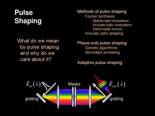
Pulses in the Zero-Spacing Limit of the GOY Model
- 格式:pdf
- 大小:470.48 KB
- 文档页数:27


1.PCM原理抽样量化与编码:sampling,quantizing and coding话路:speech channel幅值: amplitude value抽样频率: sampling frequency抽样速率: sampling rate脉冲流: stream of pulses重复率: repetition rate编码过程: coding process模拟信号: analog signal传输质量: transmission quality数字通信: digital communication数字传输: digital transmission含噪声的环境: noisy environment传输路由: transmission path信噪比 :signal-to-noise ratio信号电平 :signal levels噪声功率: noise power地面系统: terrestrial system二进制传输: binary transmission反向操作: reverse operation8-位码序列: 8-digit sequence接受端: receiving terminal帧格式 :frame format同步字 :synchronization word实现这三项功能的方案 :the schemes for performing these three functions一串幅值: a series of amplitude values电话质量的话路 a speech channel of telephone quality一个8位二进制码的序列: a sequence of 8-binary digits理论上的最小抽样频率 :a minimum theoretical sampling frequency占据着300Hz到3.4kHz频率范围的话路: a voice channel occupying the range 300Hz to 3.4kHz 每个样值8-位码: 8-digits per sample value汽车点火系统的打火: the sparking of a car ignition system重复率为64kHz的脉冲流: the stream of the pulses with a repetition rate of 64kHz真实信号与噪声信号的关系: relationship of the true signal to the noise signal由卫星上接受到的信号 :the signal received from a satellite一条特定消息中的全部信息 :the complete informatian about a particular message被传信号的波形 :the shape of the transmitted signal由传输路由引入的衰减: the attenuation introduced by transmission path将抽样的幅值转换成一串脉冲的单元 :the unit that converts sampled amplitude value to a set of pulses涉及到第一路,第二路及其他各路的序列: a sequence relating to channel 1,2 and so on被称为同步字的独特码序列: a unique sequence of pulses called synchronization word地面系统 :terrestrial system脉冲的“有”或“无” : the presence or absence of the pulses高速的电子开关: a high-speed electronic switch时分多路复用器 :the time division multiplexer时分多路复用 :Time Division Multiplexer2.异步串行数据传输串行接口 serial interface显示终端 CRT terminal发送器与接收器 transmitter and receiver数据传输 data transmission数据流 data stream闲置状态 the idle state传号电平 mark level空号电位 space level起始位 start bit停止位 stop bitT秒的持续时间 duration of T seconds奇偶校检位 parity bit错误标志 error flag传输错误 transmission error下降沿 fallinf edge符号间的空格 intersymbol space接收机的定时 receiver timing本地时钟 local clock磁带 magnetic tape控制比特 control bit逻辑1电平 logical 1 level二进制数据 binary data明显的缺点 obvious disadvantage异步串行数据传输 asynchronous serial data transmission最为流行的串行接口 the most popular serial interface所传送的数据 the transmitted data发送器与接收器的时钟 the clocks at the transmitter and receiver电传机的时代 the era of teleprinter一个字符的点和划 the dots and dashs of a character符号间空格持续时间的三倍 three times the duration of intersymbol space被称为字符的比特组 the group of bits called characters由7或8个比特的信息组成的固定单元 the invariable units comprising 7 or 8 bits of information 由接收机本地产生的时钟 a clock generated locally by the receiver在字符后所收到的奇偶校检位 the received parity bit following the character起始位的下降沿 the falling edge of the start bit数据链路面向字符的特性 the character-oriented nature of the data link3.数据通信地下电缆 underground cable通信卫星 communication satellite微波设备 microwave facilities调制器与解调器 modulator and demodulator缓冲器 buffer定时信号 timing signals同步脉冲 synchronization pulses时隙 time slot移位寄存器 shift register传输媒体 transmission medium线形衰弱 linear attenuation信息安全 information security键盘 keyboard数据终端 data terminals某种类型的数据转换设备 some type of data conversion equipment视频显示终端 visual display terminal称为数据调制解调器的双向数据发送接收机 two-way data transmistter-receiver called a data modem 全双工的数据传输系统 full-duplex data trandmission system由数据处理器的运算速率所决定的速率 the rate determined by the operating speed of the data processor由接口部件来的定时信号 timing signals from the interface assembly磁心存储器 magnetic core memories线性衰减和时延特性 linear attenuation and delay characteristics传输损伤 transmission impairments语音中的冗余特性 the redundant nature of speech在数据发送器中的编码过程 coding process in the data transmitter二进制的不归零信号 binary nonreturn-to-zero signal4.互联网网络资源:network resource信息服务:information services远程终端:remote terminals互联的系统:interconnected systems命令:command电子邮件:electronic mail主机:host无线信道:wireless channels搜索工具:searching tools用户界面:user interface存取:access文本信息:textual messages协议:protocol超文本协议:hypertext protocol分布在全世界的计算机的巨大网络:gaint network of computers located all over the world主干系统:backbone system全国范围的网络:nationwild network电子会议:electronic conferences实时对话:live conversation最大的信息库the largest repository of the computers on the net网络设备资源:network facilities resources在网上的绝大多数计算机:the vast majority of the computer on the netUNIX操作系统:the UNIX operating system在因特网和你的PC机之间传送数据的方法:a way to move data between the internet and your PC 方便的搜索工具:the convenient searching tools联网的超文本协议:the network hypertext protocol5.光纤通信介绍光纤通信:optical fiber communications光源:light source波长:wavelength激光器:laser色散:dispersion传输介质:transmission medium多模光纤:multi-mode fiber长途干线:long-houl trunks单模光纤:singer-mode fiber带宽:bandwidth带宽用户:wideband subscriber纤维光学:fiber-optics商用技术:commercial technologe门限电流:threshod current光检测器:photodetector波分复用:wavelength multiplexing纤维光网络:fiber-optic network视频带宽:video bandwidth长途传输:long distance transmission中继距离:repeater spacing已装光纤的总长度:the total length of installed fiber长途通信系统:long-haul telecommunication system低衰减的石英纤维:the low-loss silica fiber衰减接近瑞利极限的光纤:fibers with losses approaching the Rayleigh limit室温下的门限电流:room temperature threshold currents较长波长区:the longer wavelength region用户接入工程:subscriber access project部件性能和可靠性的改进:improvements in component performance and reliability已安装的光纤系统的数据速率:data rates for installed fibre optic system每秒吉比特:gigabit per second range波分复用:wavelength multiplexing带宽用户环路系统:widebend subscriber loop system多纤连接器:multifibre connectors设计寿命:projected lifetime光源:light source单模光纤:single-mode fibre分布反馈式激光器:distributed-feedback laser信息容量:information capacity交换体系:switching hierarchy带宽业务:broadband services9.蜂窝式移动电话系统蜂窝式移动电话:cellular mobile telephone服务性能:services performance频谱:frequency spectrum频带:frequency band微处理器:microprocessor移动手机:mobile unit广播业务:broadcast servise天线:antenna子系统:subsystems移动用户:mobile subscriber服务能力:service capability利用率:utilization带宽:bandwidth单边带:single-sideband扩频:spread spectrum大规模集成电路:large scale integrated circuits蜂窝点:cellular site蜂窝交换机:cellular switch无线机架:radio cabinet呼叫处理:call processing频谱利用率:frequency spectrum utilization有限的指定频带:the limited assigend ferquency band 服务区:servise area复杂的特性和功能:complicated features and functions大规模集成电路技术:large-scale integraesd circuit technology试验性的蜂窝系统:developmental cellular system中央协调单元:central coordinating element蜂窝管理:cellular administration传统移动电话的运行限制:operational limitiation of conventional mobile telephone system 有限的服务能力:limitied service capability无线通信行业:radio communcation industry可用的无线电频谱:available radio frequency spectrum所分配的频带:the allocated frequency band移动收发信机:mobile transceiver技术上的可行性:techological feasibility严格的频谱限制:severe spectrum limitations调频广播业务:FM broadcasting services传播路径衰耗:propagration path loss多径衰耗:multipath fading电话公司地方局:telephone company zone offices10.全球移动通信系统个人通信 personal communcation通信标准 communcation standrads固定电话业务 fixed telephone services网络容量 network capability移动交换中心 mobile switching center国际漫游 international roaming宽带业务 broadband services接口转换 interface conversion频谱分配 frequency allocation模拟方式 analogue mode蜂窝通信原理 cellular communcation principe拥塞 jamming蜂窝裂变 cellular splitting基站 base station寄存器 register收费功能 billing function接入方法 access method突发脉冲传输方式 brusty transimission mode开销信息 overhead information切换算法 handover algorithms短消息服务 short message services技术规范 technical specificationtotal access communcation system 全接入的通信系统global mobile communcation system 全球移动通信系统time division multiple access 时分多址facsimile and short message services 传真和短消息服务fixed communcation networks 固定通信网络a more personalized system 更加个性化的系统the cost and quality of the link 链路的价格和质量market growth 市场的发展fixed telephone service 固定电话服务coxial cable 同轴电缆interface convision 接口转换cellular communcation priciple 蜂窝通信原则frequency reuse and cell splitting 频率复用和蜂窝裂变cochannel interference 共信道干扰theoretical spectual capability 理论上的频谱容量micro-cellular system 微蜂窝系统base station transceiver 基站收发信机subscriber register 用户寄存器burst transmission mode 突发脉冲传输模式overhead information 开销信息advanced handover algorithms 先进的切换算法facsimile and short message services 传真和短消息服务the GSM technique specications GSM技术规范说明一1 . 研究二进制的传输可见, 只要简单地去判别脉冲的“有”和“无”, 我们就获得了一条消息的全部信息。

Unit 1 The Principle of PCM 请将下述词组译成英文1、抽样量化与编码sampling , quantizing and coding2、话路speech channel3、幅值amplitude frequency4、抽样频率sampling frequency5、抽样速率sampling rate6、脉冲流stream of pulses7、重复率repetition rate8、编码过程coding process9、模拟信号analog signal10、传输质量transmission quality11、数字通信digital communication12、数字传输digital transmission13、含噪声的环境noisy environment14、传输路由transmission path15、信噪比Signal-to-noise ratio16、信号电平signal levels17、地面系统terrestrial system18、噪声功率noise power19、二进制传输binary transmission20、反向操作reverse operation21、8位码序列8-bit sequence22、接收端receiving terminal23、帧格式frame format24、同步字synchronization word 请将下述词组译成中文1、the schemes for performing these three functions实现这三项功能的方案2、 a series of amplitude values一串幅值3、 a speech channel of telephone quality电话质量的话路4、 a sequence of 8-binary digits一个8位二进制码的序列5、 a minimum theoretical sampling frequency理论上的最小抽样频率6、 a voice channel occupying the range 300 Hz to 3.4kHz占据着300Hz到3.4kHz频率范围的话路7、8-digits per sample value每个样值8位码8、the sparking of a car ignition system汽车点火系统的打火9、the stream of the pulses with a repetition rate of 64kHz重复率为64kHz的脉冲流10、the relationship of the true signal to the noisesignal真实信号与噪声信号的关系11、the signal received from a satellite由卫星上受到的信号12、the complete information about a particular message一条特定消息中的全部信息13、the shape of the transmitted signal被传信号的波形14、the attenuation introduced by transmission path由传输路由引入的衰减15、the unit that converts sampled amplitude value to a setof pulses将抽样的幅值转换成一串脉冲的单元16、a sequence relating to channel 1,2 and so on涉及到第一路、第二路及其他各路的序列17、a unique sequence of pulses called synchronizationword被称为同步字的独特的码序列18、terrestrial system地面系统19、the presence or absence of the pulse脉冲的“有”或“无”20、a high-speed electronic switch高速的电子开关21、the time division multiplexer时分多路复用器22、Time Division Multiplexing时分多路复用Unit 2 Asynchronous Serial Data Transmission请将下述词组译成英文1、串行接口serial interface2、显示终端CRT terminal3、发送器与接收器transmitter and receiver4、数据传输data transmission5、数据流data stream6、闲置状态the idle state7、传号电平mark level8、空号电平space level9、起始位start bit10、停止位stop bit11、T秒的持续时间duration of T seconds12、奇偶校验位parity bit13、错误标志error flag14、传输错误transmission error15、下降沿falling edge16、符号间的空格intersymbol space17、接收机的定时receiver timing18、本地时钟local clock19、磁带magnetic tape20、控制比特control bit21、逻辑1电平logical 1 level22、二进制数据binary data23、明显的缺点obvious disadvantage请将下述词组译成中文1、asynchronous serial data transmission异步串行数据传输2、the most popular serial interface最为流行的串行接口3、the transmitted data所传送的数据4、the clocks at the transmitter and receiver发送器和接收器的时钟5、the era of teleprinter电传机的时代6、the dots and dashes of a characters一个字符的点和划7、three times the duration of intersymbol space符号间空格持续时间的三倍8、the group of bits called characters被称为字符的比特组9、the invariable units comprising 7 or 8 bits of information由7或8个比特的信息组成的固定单元10、a clock generated locally by the receiver由接收机本地产生的时钟11、the received parity bit following the character在字符后接收到的奇偶校验位12、the falling edge of the start bit起始位的下降沿13、the character-oriented nature of the data link数据链路面向字符的特性Unit 3 The ISO Networking Standards请将下述词组译成英文1、联网技术networking technology2、国际标准化组织the International Organization for Standardization3、参考模型reference model4、数据分组data packets5、应用程序application program6、网络媒体network media7、分层layering8、硬件和软件hardware and software9、表示层the presentation layer10、传输层the transport layer11、数据链路层the data link layer12、网络服务network services13、文件接入file-access14、数据格式the data format15、主机host16、协议protocol17、连接connectivity18、逻辑选址logical addressing请将下述词组译成中文1、networking technology联网技术2、proprietary networking system专用网络系统3、the International Organization for Standardization国际标准化组织4、compatibility between the various types of networks各种网络之间的兼容性5、seven numbered layers七层6、standardization of network components网络部件的标准化7、error recovery纠错8、receiving host’s system接收方的主机系统9、connection-oriented circuits面向连接的电路10、information flow control信息流的控制11、network topology网络拓扑12、network media access网络媒体接入13、electrical specification电气标准14、maximum transmission distance最大传输距离Unit 4 The TCP/IP Reference Model请将下述词组译成英文1、传输控制协议transmission control protocol2、互联协议internet protocol3、数据通信data communication4、微波microwave5、高层协议higher-level protocol6、流量控制traffic control7、目的地destination8、(信)源resource9、段segment10、互联层Internet layer11、分组交换packet switching12、超文本传输协议hypertext transfer protocol13、灵活性flexibility14、数据报datagram请将下述词组译成中文1、transmission control protocol传输控制协议2、internet protocol互联协议3、satellite links卫星链路4、the standard on which the internet has grown互联网发展所基于的标准5、network access layer网络接入层6、connection-oriented protocol面向连接的协议7、file transfer protocol文件传输协议8、hypertext transfer protocol超文本传输协议9、domain name system域名系统10、developer of software软件开发人11、user datagram protocol用户数据报协议12、packet-switched technology分组交换技术Unit 5 Local-Area Networks (1)请将下述词组译成英文1、局域网local area network2、工作站workstation3、外设peripheral4、拓扑topology5、集线器hub6、交换器switch7、流量traffic8、网络接口卡network interface card9、数据库database10、印刷电路板printed circuit board11、主板motherboard12、网络适配器network adapter13、并行数据parallel data14、电脉冲electrical impulses15、中继器repeater16、联网介质networking media请将下述词组译成中文1、local-area network局域网2、logical topology逻辑拓扑3、devices that connect directly to a network segment 直接连到网络段的部件4、network interface card网络接口卡5、process of the encapsulation打包的过程6、standardized symbol标准化的符号7、printed circuit board印刷电路板8、expansion slot of a bus on a computer’s motherboard在计算机母板上总线的扩展槽9、network adapter网络适配器10、parallel signal produced by the computer由计算机产生的并行信号11、transmitting station发送站12、the specifications for Category 5 twisted-pair Ethernet五类双绞线以太网的规范Unit 6 Local-Area Networks (2)请将下述词组译成英文1、无源集线器passive hub2、网桥bridge3、可用带宽useable bandwidth4、地址表addressing table5、交换器switch6、路由器router7、光纤optical fiber8、无线介质wireless media9、铜线copper wire请将下述词组译成中文1、the device that serves as the center of a network作为网络中心的部件2、multi-port repeater多端口中继器3、reliability of the network网络的可靠性4、passive or active hubs无源或有缘的集线器5、protocol address or network address地址或网络地址6、network administrator网络管理者7、switching of packets to the best route交换分组到最佳路由8、network segment网络段Unit 7 Internet请将下述词组译成英文1、网络资源network resource2、信息服务information services3、远程终端remote terminals4、地址address5、互联的系统interconnected systems6、命令command7、电子邮件electronic mail8、主机host9、无线信道wireless channels10、搜索工具searching tools11、用户界面user interface12、拷贝copy13、互联网internet14、存取access15、文本信息textual messages16、鼠标mouse17、协议protocol18、超文本协议hypertext protocol请将下述词组译成中文1、giant network of computers located all over the world分布在全世界的计算机的巨大网络2、backbone system主干系统3、nationwide network全国范围的网络4、electronic conference电子会议5、remote terminal远程终端6、live conversation实时的对话7、world wide web万维网8、searching tool搜索工具9、the largest repository of information最大的信息库10、network facilities resources网络设备资源11、the vast majority of the computers on the net在网上的绝大多数计算机12、the Unix operating systemUnix 操作系统13、textual messages文本信息14、 a way to move data between the internet and your PC 在因特网和你的PC机之间传送数据方法15、the convenient searching tools方便的搜索工具16、the networked hypertext protocol联网的超文本协议Unit 8 Introduction to Optical Fiber Communication 请将下述词组译成英文1、光纤通信optical fiber communications2、光源light source3、波长wavelength4、激光器laser5、色散dispersion6、传输介质transmission medium7、多模光纤multi-mode fiber8、长途干线long-haul trunks9、单模光纤single-mode fiber10、带宽bandwidth11、宽带用户wideband subscriber12、纤维光学fiber-optics13、商用技术commercial technology14、门限电流threshold current15、光检测器photodetector16、波分复用wavelength multiplexing17、纤维光网络fiber-optic networks18、视频带宽video bandwidth请将下述词组译成中文1、long distance transmission长途传输2、repeater spacing中继距离3、commercial technology商用技术4、optical fiber communications光纤通信5、the total length of installed fiber已装光纤的总长度6、long-haul telecommunication system长途通信系统7、the low-loss silica fiber低衰减的石英纤维8、fibers with losses approaching the Rayleigh limit衰减逼近瑞利极限的光纤9、room temperature threshold currents温室下的门限电流10、the longer wavelength region较长波长区11、subscriber access project用户接入工程12、improvements in component performance andreliability部件性能和可靠性的改进13、data rates for installed fiber optic system已安装的光纤系统的数据速率14、gigabit per second range每秒吉比特15、wavelength multiplexing波分复用16、wideband subscriber loop system宽带用户环路系统17、multifiber connectors多纤连接器18、projected lifetime设计寿命19、light source光源20、single-mode fiber单模光纤21、distributed-feedback laser分布反馈式激光器22、information capacity信息容量23、switching hierarchy交换体系24、broadband services宽带业务Unit 9 Cellular Mobile Telephone System请将下述词组译成英文1、蜂窝式移动电话cellular mobile telephone2、服务性能service performance3、频谱frequency spectrum4、频带frequency band5、微处理器microprocessor6、移动手机mobile unit7、广播业务broadcast service8、天线antenna9、子系统subsystems10、移动用户mobile subscriber11、服务能力service capability12、服务性能service performance13、利用率utilization14、带宽bandwidth15、单边带single-sideband16、扩频spread spectrum17、大规模集成电路large scale integrated circuits18、蜂窝点cellular site19、蜂窝交换机cellular switch20、无线机架radio cabinet21、呼叫处理call processing22、服务区service area请将下述词组译成中文1、frequency spectrum utilization频谱利用率2、the limited assigned frequency band有限的指定频带3、complicated features and functions复杂的特性和功能4、large-scale integrated circuit technology大规模集成电路技术5、developmental cellular system实验性的蜂窝系统6、central coordinating element中央协调单元7、cellular administration蜂窝管理8、operational limitation of conventional mobiletelephone system传统移动电话的运行限制9、limited service capability有限的服务能力10、radio communication industry无线通信行业11、available radio frequency spectrum可用的无线电频谱12、the allocated frequency band所分配的频带13、mobile transceiver移动收发信机14、technological feasibility技术上的可行性15、severe spectrum limitations严厉的频谱限制16、FM broadcasting service调频广播业务17、propagation path loss传播路径衰耗18、multipath fading多径衰耗19、radio cabinet无线机架20、telephone company zone offices电话公司地方局Unit 10 GSM ( Global System for MobileCommunication )请将下述词组译成英文1、个人通信personal communcations2、通信标准communication standards3、固定电话业务fixed telephone service4、网络容量network capacity5、移动交换中心mobile switching center6、国际漫游international raoming7、宽带业务broadband services8、接口转换interface conversion9、频谱分配frequency allocation10、模拟方式analogue mode11、蜂窝通信原理cellular communication principle12、拥塞jamming13、蜂窝裂变cell splitting14、基站base station15、寄存器register16、收费功能billing function17、接入方法access method18、突发脉冲传输方式burst transmission mode19、开销信息overhead information20、切换算法handover algorithms21、短消息服务short message service22、技术规范technical specification请将下述词组译成中文1、total access communication system全接入的通信系统2、global mobile communication system全球移动通信系统3、time division multiple access时分多址4、facsimile and short message service传真和短信息服务5、fixed communication networks固定通信网络6、 a more personalized system更个人化的系统7、the cost and quality of the link链路的价格与质量8、market growth市场的发展9、fixed telephone service固定电话业务10、coaxial cable同轴电缆11、interface conversion接口转换12、cellular communication principle蜂窝通信原理13、frequency reuse and cell splitting频率再用和蜂窝裂变14、cochannel interference共信道干扰15、theoretical spectral capability理论上的频谱容量16、micro-cellular system微蜂窝系统17、base station transceiver基站收发信机18、subscriber register用户寄存器19、burst transmission mode突发脉冲传输模式20、overhead information开销信息21、advanced handover algorithms先进的切换算法22、the GSM technical specificationsGSM的技术规范Unit 11 Circuit Switching and Packet Switching请将下述词组译成英文1、电路交换circuit switching2、分组交换packet switching3、报文交换message switching4、子网subnet5、信头header6、目的地址destination address7、误差控制error control8、存储转发方式store-and-forward manner9、突发性bursty10、传输时延transmission delay11、中间交换设备intermediate switching equipment12、交换技术switching technique13、返回信号return signal14、报文处理机message processor15、给定最大长度given maximum length16、信息转移information transfer17、随机性random18、专用电路dedicated circuit19、电路利用率channel utilization请将下述词组译成中文1、the capability of storing or manipulating user’s data存储和处理用户数据的能力2、the special signaling message特定的信令信息3、 a well defined block of data called a message被精心定义的称为报文的数据块4、the information regarding the source and destinationaddresses涉及源和目的地址的信息5、the computer referred to as a message processor叫做报文处理器的计算机6、the store-and-forward transmission technique存储转发传输技术7、the dynamic allocation of the bandwidth宽带的动态分配8、the overall transmission delay of the message报文整个的传输时延9、switching technique交换技术10、circuit switching电路交换11、message switching报文交换12、packet switching分组交换13、total path of connected lines连线的整个通路14、source-destination pair源到目的地的一对15、communication parties通信各方16、transmission unit传输单元17、initial connection cost incurred in setting up the circuit在建立电路时产生的起初连接成本18、low delay constraint required by the user用户所需的短时延的限制19、the fixed dedicated end-to-end circuit固定专用的端到端电路20、low channel utilization低的电路利用率Unit 12 ATM请将下述词组译成英文1、异步转移模式asynchronous transfer mode2、逻辑信道logical channel3、虚电路virtual circuits4、虚路径virtual path5、建议recommendation6、网络层network level7、业务与应用层service and application level8、虚连接virtual connection9、信息高速公路information superhighway10、点播电视video-on-demand11、统计复用statistical multiplexing12、数字化的信息digital information13、标识符identifier14、协议protocols15、网络节点network node16、宽带网broadband network17、ATM论坛ATM forum18、面向未来的future-proofed19、图像编码image encoding20、虚拟专用网virtual private network21、数据处理data processing请将下述词组译成中文1、short packets called cells被叫做信元的短的分组2、bit rates of several hundred megabits a second每秒几百兆比特的速率3、unique multiplexing method独特的复用方法4、the physical connection between any two terminals任何两个终端之间的物理连接5、interactive video services交互式的视频业务6、 a nature vehicle for multimedia services多媒体业务的自然载体7、the current and future requirements of both operatorsand users运营者和用户当期和未来的要求8、the technique for switching high bit rate channel高比特率信道的交换技术9、asynchronous transfer mode异步转移模式10、multiplexing and switching technique复用和交换技术11、the underlying type of transmission所承载的传输类型12、dual identification双重标识13、virtual circuit虚电路14、virtual path虚路径15、the transfer of cells to the network nodes信元在网络节点上的转移16、hundreds megabits a second每秒几百兆比特17、recommendation I.121I.121建议18、the quality of service服务质量19、in proportion to the exact requirement与实际需求成比例20、the applications and services transported over anetwork网络所传送的应用和业务21、the ability to construct virtual networks构成虚网络的能力22、cost-effective use of infrastructure低价高效的利用网络设施23、future-proofed面向未来的24、coordinating different networks carrying differentservices协调传送不同业务的不同网络25、essential components of future informationsuperhighways未来的信息高速公路的基本部件26、statistical multiplexing统计复用27、optimum use of resources资源的最佳使用28、virtual private networks虚拟专用网Unit 13 The Public Telecommunications Network请将下述词组译成英文1、公众电信网public telecommunication network2、本地环路local loop3、交换节点switching node4、双绞线twisted pair5、外部呼叫external call6、端局end office7、数字数据系统digital data systems8、二线连接two wire connection9、收费中心toll center10、电路交换网circuit-switched network11、电话用户telephone subscriber12、数据流量data traffic13、链路link14、中继线trunk15、半双工的half-duplex16、全双工的full-duplex17、中间交换节点intermediate switching node18、音频电路voice-frequency circuit19、汇接交换机tandem switch20、外部呼叫external call21、拓扑topology22、节点间的internode23、路由route请将下述词组译成中文1、full-duplex connection全双工的连接2、the function of concentrating traffic集中话务量的功能3、the switching nodes called tandem switches被称为汇接局的交换节点4、 a fraction of subscribers一小部分用户5、the interface between the station and the network在站和网络之间的接口6、the subscriber that transmit digital signal发送数字信号的用户7、national networks国家网络8、architectural components结构部件9、local loop本地环路10、the branches between nodes节点间的支路11、twisted pair双绞线12、full duplex全双工的13、intermediate switching nodes中间交换节点14、tree topology树状拓扑15、transmission facilities传输设备16、multiple voice-frequency circuits多条音频电路17、synchronous TDM同步时分复用18、adjacent end offices相邻的端局19、full connectivity全连通性20、isolated subnetworks被分离开的子网21、high-usage trunks高效中继线22、basic order of selection路由选择的基本次序23、backbone hierarchical network主干体系网络24、two subscribers attached to different end offices连到不同端局的两个用户25、exchange area交换区Unit 14 Integrated Services Digital Network请将下述词组译成英文1、全球通信global communication2、灵活性flexibility3、端到端的数字连接end-to-end digital connectivity4、开放网络open network5、语声编码voice encoding6、综合业务数字网integrated services digital network7、系统结构infrastructure8、全球通信global communication9、国际标准化组织International Organization for Standardization10、通信载体communication carriers11、传输媒质transmission medium12、接口设备interface equipment13、宽带限制bandwidth limitation14、交换设备switching equipment15、语音编码voice encoding16、脉码调制pulse code modulation17、基本接入basic access请将下述词组译成中文1、the integrated services digital network综合业务数字网2、the International Organization for Standardization国际标准化组织3、degradation due to the transmission medium由于传输媒质导致的质量下降4、bandwidth limitations inherent in a 4 kHz voicechannel4kHz话路中所固有的带宽限制5、standardized ports标准化的接口6、pulse code modulation脉码调制7、digital communication数字通信8、ISDN standards and system architectureISDN的标准和系统结构9、global communications全球通信10、progressive application of digital technology数字技术的逐步应用11、public communication carriers公共通信载体12、enhanced quality高质量13、substantial quantity of interface equipment 大量的接口设备14、flexibility in the transmission of voice, data, video andother services在传送话音、数据、视频和其他业务上的灵活性15、bandwidth limitations带宽的限制16、end-to-end digital connectivity端到端的数字连接17、voice encoding techniques语音编码技术18、pulse coding modulation脉码调制19、basic access signaling rate基本接入信令速率20、universal access统一的接入21、experimental technology实验性的技术Unit 15 Current Situation and the Future in theTelecommunication World请将下述词组译成英文1、X.25协议X.25 protocol2、电视信号television signals3、窄带业务narrowband services4、基本接入basic access5、电信业务teleservice6、用户电报telex7、无线电波radio waves8、地面天线ground antenna9、同轴的coaxial10、直接广播系统direct broadcast system11、端到端的时延end-to-end delay12、抖动jitter13、繁忙小时peak hours14、芯片技术chip technology15、高清晰度电视high definition television16、运行与维护operations and maintenance请将下述词组译成中文1、the existing public network现有的公用网络2、classical two-way voice conversation传统的双向对话3、packet switched data network based on X.25 protocols基于X.25协议的分组交换数据网络4、the user access to the network对网络的用户接入5、 a circuit switched service with a channel rate of 70Mbit/s信道速率为70Mbit/s的电路交换业务6、the service-independent network与业务无关的网络7、the optimal statistical sharing of the resources对资源的最佳统计复用8、telecommunication service电信业务9、telex network用户电报网10、messages of characters文字报11、two-way voice conversation双向对话12、X.21 protocolsX.21协议13、ground antenna地面天线14、coaxial tree network同轴树状网络15、community antenna TV network公用天线的电视网络16、direct broadcast system直接广播系统17、Ethernet以太网18、token bus and token ring network令牌总线网和令牌环网19、end-to-end delay端到端的时延20、world-wide independent networks全球范围的独立网络21、the peak hours in the telephone network电话网络的繁忙小时22、resource pooling资源共享23、peak hour traffic繁忙小时流量24、integration of narrow-band services窄带业务的综合25、the progress in speech coding and chip technology 在语声编码和芯片技术方面的进步26、 a new teleservice新的电信业务27、adapting to new service requirements对新业务要求的适配28、optimal statistical sharing of the resources资源最佳统计式的共享。

Supertex inc.AN-H56Application NoteIntroductionThe MD1812 and the MD1813 are two unique composite return-to-zero (RTZ) pulser drivers for ultrasound applications. The ICs have built-in level shifters that provide negative P-MOS gate DC bias and fast AC coupled gate drivesignals. They enable the fast damping functions necessary to generate return-to-zero bipolar pulses, and are also able to keep the zero-state to as long as needed, even to infinity. These kinds of fast return-to zero and DC coupled features are very useful for medical ultrasound imaging equipment, piezoelectric transducer drivers, material flaw detection, ultrasonic NDT detection, and sonar ranger applications, especially for those that need to launch ultrasound in pseudo-random codes. Designing a Pulser with the MD1812/13This a pplication n ote d escribes h ow t o u se M D1812 o r M D1813 to design the basic channel of an ultrasound transmitter with the RTZ feature. The circuit is a single channel ultrasound transmitter using the MD1812 or MD1813 to drive TC6320 & TC2320 MOSFETs. It can generate fast return to zero waveforms. The output of high voltage to transducer has ±2A source and sink current capability. A CPLD programmable logic circuit and on-board 40MHz crystal oscillator generate a fast logic signal to control the pulse circuit. The CPLD hasa six-pin JTAG connection for Xilinx’s USB or a convenient parallel-port programming link cable. The circuit consists of one MD1812K6 or MD1813K6 in a 16-lead 4x4x0.9mm QFN package, driving TC6320FGs and TC2320FGs, two complementary high-voltage P and N- channel MOSFETs in one single SO-8 package. The input stage of the MD1812/13 is a high-speed level translator that is able to operate with logic input signals of 1.2V to 5.0V amplitude. In this circuit, the CPLD output logic is typically 3.3V. An adaptive threshold circuit is used with the OE pininside of the MD1812 to set the level translator threshold to the middle of the input logic 0 and logic 1 levels. The OE pin serves a dual purpose. First, its logic 1 level is used to compute the threshold voltage level for the channel input level translators. Second, when OE is low, the outputs are disabled, with the A and C outputs high and the B and Doutputs low (for MD1812 only). This assists in properly pre-charging the coupling capacitors that may be used in series in the gate drive circuit of external PMOS and NMOS FETs. The MD1812/13 level translator uses a proprietary composite drive circuit, which provides DC coupling, together with high-speed operation. The output pin, OUT C , is designed to drive the return-to-zero PMOS FET through a capacitor as fast as an AC coupling gate driver, and OUT G provides delayed DC coupling negative biased gate control to the same PMOS FET. The OUT C swings between V H and V L voltages, while OUT G is within V SS or V NEG levels. Note that the OUT C and OUT G pins of one chip are designed to drive together forone PMOS FET, and that the PMOS FET source is typicallyconnected to the same potential of the MD1812/13 V SS voltage. Each of the output stages of OUT A , OUT B , OUT C & OUT D of MD1812/13 are capable of peak currents of up to ±2.0A, depending on the supply voltages used and load capacitance. But a 2kΩ resistor, R36, must be between OUT G and the gate of the PMOS FET, which is driven by the OUT C through a capacitor. This configuration provides the optimal series resistance value of the gate DC bias driver circuit.The output stage of the MD1812/13 has separate power connections enabling the output signal high and low levels to be chosen independently from the driver supply voltages. As an example, the input logic levels may be 0V and 1.8V, the control logic may be powered by +5V and –5V, and the output high and low levels may be varied anywhere over the range of +5V to -5V. In this design example, MD1812/13’s V DD and V H are both powered by +10V, V SS and V L are grounded, and V NEG is –10V. The source pin of the RTZ PMOS FET driven by the OUT C and OUT G pins is connected to ground.PCB Layout TechniquesIt is very important that the slab at the bottom of the IC package, which is the IC substrate “pin”, be externally connected to the V NEG pin to make sure it always has the lowest potential in any condition.Designing An Ultrasound Pulser with MD1812/MD1813 Composite DriversBy Ching Chu, Sr. Application EngineerUse high-speed PCB trace design practices that are compatible with the circuit’s operating speed. The internal circuitry of the MD1812/13 can operate at up to 100MHz, with the primary speed limitation being due to load capacitance. Because of this high speed and the high transient currents that result when driving capacitive loads, the supply voltage bypass capacitors should be as close to the supply pins as possible. The V SS and V L pins should have low inductance feed-through connections that are connected directly to a solid ground plane. If these voltages are not zero, they will require bypass capacitors similar to the positive power supplies. The V DD and V H supplies determine the output logic levels. These two pins can draw fast transient currents of up to 2.0A, so they should be provided with a low-impedance bypass capacitor at the chip’s pins. A ceramic capacitor of up to 1.0µF may be appropriate. Minimize the trace length to the ground plane, and insert a ferrite bead in the power supply lead to the capacitor to prevent resonance in the power supply lines. A common voltage source and local decoupling capacitor may be used for the V DD and V H pins, which should always have the same DC level applied to them. For applications that are sensitive to jitter and noise, insert another ferrite bead between V DD and V H and decouple each pin separately.Pay particular attention to minimizing trace lengths and using sufficient trace width to reduce inductance. Surfacemount components are highly recommended. Since the output impedance of this driver is very low, in some cases it may be desirable to add a small value resistor in series with the output to obtain better waveform integrity at the load terminals. This will, of course, reduce the output voltage slew rate at the terminals of a capacitive load. Pay particular attention to the parasitic coupling from the driver’s output to the input signal terminals. This feedback may causeoscillations or spurious waveform shapes on the edges of signal transitions. Since the input operates with signals down to 1.2V, even small coupling voltages may cause problems. Use of a solid ground plane and good power and signal layout practices will prevent this problem. Also ensure that the circulating ground return current from a capacitive load cannot react with common inductance to create noise voltages in the input logic circuitry.Testing the Ultrasound Pulser The MD1812 RTZ pulser design example is tested with the following power supply voltage and current limiting: V PP 0 to +100V 5mA, V NN 0 to -100V 5mA, V DD = +10V 50mA, V NEG -10V 5mA, V CC +3.3V, 90mA.The HV OUT signal appears at the SMA connector J6. There is a 5:1 attenuation of the signal, due to the value of resistor R11. When driving a real transducer load, the value of this resistor should be reduced in value to match the load impedance.The HV OUT signal passes through jumper J5, which can be used to terminate the HV OUT signal in a dummy load, comprising a 220pF capacitor in parallel with a 1kΩ resistor. When an external load is connected, the dummy load is not required, and J5 can be configured to pass the signals straight through to the output connector J6.All the on-board test points are designed to work with an active oscilloscope probe, such as the Tektronix P6243 1MΩ active probe. Because TP7 is connected to the HV OUT , where potentially damaging voltages could be present, make sure that V PP /V NN does not exceed the probe limit. If using another type of high impedance oscilloscope probe for the test points, ensure that the ground lead connections to the circuit board ground plane are as short as possible.There are multiple frequency and waveform combinations that can be selected as bipolar pulses, PW or CW waveforms. An external clock input can be used if the on-board 40MHz-oscillator is disabled. The external trigger input can be used to synchronize the output waveforms. There are five push buttons for selecting demo waveform, frequency, phase, and MD1812 chip enable functions. Color LEDs indicate the demo selection states. The CH1 output allows the monitoring of one of the 5 inputs (IN A , IN B , IN C , IN D or O E ) of the MD1812/13 via the select button. The MD1812 and the MD1813 are very similar in function. The only differences between them are the control of the OE (MD1812) vs VLL (MD1813) pin and their logic functions. Please read their data sheets for the details. In this design example, the CPLD program is using an on-board solder jumper, R34, to sense the difference and works accordingly. The example MD1812/13 pulser circuit schematic, detailsignals definitions, and some measured waveforms areshown below.Waveform C, 20MHz, 8 cycles Load: 220pF//1kPulser Circuit SchematicWaveform AWaveform CWaveform BWaveform DOE INA INB INC INDHV OUTV PPV NNOE INA INB INC INDHV OUTV PPV NNOE INAINBINC INDHV OUTV PPV NNOEINAINBINC IND HV OUTV PPV NNNote: The duty cycle of the PW burst is set about 0.2% for limitedpower dissipationNote: The duty cycle of the PW burst is set about 25% at ≤5.0MHz forlimited power dissipation.AN-H56MD1812/13 Reference DesignJ 6X D C RJ E X = L oFig. 1 Waveform of 2.5MHz Fig. 2 Waveform of 5MHzFig. 3 Waveform of 10MHz Fig. 4 Waveform of 10MHz InvertingFig. 5 Waveform of 20MHz 8 Cycles Fig. 6 Waveform of 5mHz & Delay ReadingsFig. 7 Waveform of 10MHz(at IN C , OUT C , OUT G , and P- Gate, V DD = 12V, V NEG = -10V)Fig. 8 Waveform of 5MHz(at IN C , OUT C , OUT G , and P- Gate, V DD = 5V, V NEG = -10V)Supertex inc. does not recommend the use of its products in life support applications, and will not knowingly sell them for use in such applications unless it receives an adequate “product liability indemnification insurance agreement.” Supertex inc. does not assume responsibility for use of devices described, and limits its liability to the replacement of the devices determined defective due to workmanship. No responsibility is assumed for possible omissions and inaccuracies. Circuitry and specifications are subject to change without notice. For the latest product specifications refer to the Supertex inc. (website: http//)©2013 Supertex inc.All rights reserved. Unauthorized use or reproduction is prohibited.Supertex inc.。
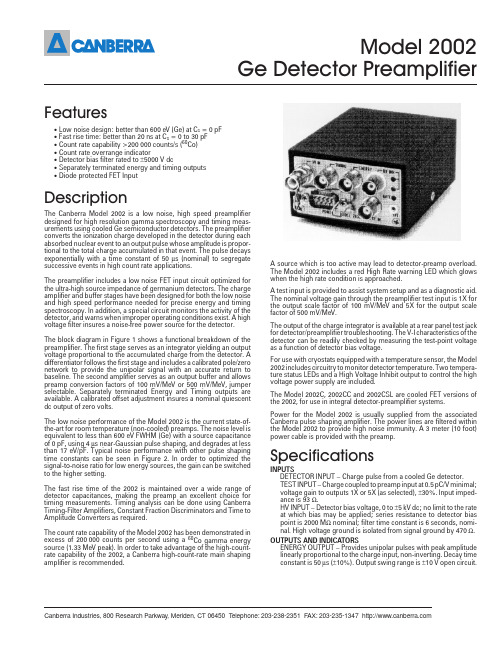
Model2002Ge Detector PreamplifierFeatures•Low noise design:better than600eV(Ge)at C s= 0pF•Fast rise time:better than20ns at C s=0to30pF•Count rate capability>200000counts/s(60Co)•Count rate overrange indicator•Detector bias filter rated to±5000V dc•Separately terminated energy and timing outputs•Diode protected FET InputDescriptionThe Canberra Model2002is a low noise,high speed preamplifierdesigned for high resolution gamma spectroscopy and timing meas-urements using cooled Ge semiconductor detectors.The preamplifierconverts the ionization charge developed in the detector during eachabsorbed nuclear event to an output pulse whose amplitude is propor-tional to the total charge accumulated in that event.The pulse decaysexponentially with a time constant of50µs(nominal)to segregate successive events in high count rate applications.The preamplifier includes a low noise FET input circuit optimized for the ultra-high source impedance of germanium detectors.The charge amplifier and buffer stages have been designed for both the low noise and high speed performance needed for precise energy and timing spectroscopy.In addition,a special circuit monitors the activity of the detector,and warns when improper operating conditions exist.A high voltage filter insures a noise-free power source for the detector.The block diagram in Figure1shows a functional breakdown of the preamplifier.The first stage serves as an integrator yielding an output voltage proportional to the accumulated charge from the detector. A differentiator follows the first stage and includes a calibrated pole/zero network to provide the unipolar signal with an accurate return to baseline.The second amplifier serves as an output buffer and allows preamp conversion factors of100mV/MeV or500mV/MeV,jumper selectable.Separately terminated Energy and Timing outputs are available.A calibrated offset adjustment insures a nominal quiescent dc output of zero volts.The low noise performance of the Model2002 is the current state-of-the-art for room temperature(non-cooled)preamps.The noise level is equivalent to less than600eV FWHM(Ge)with a source capacitance of0pF,using4µs near-Gaussian pulse shaping,and degrades at less than17eV/pF.Typical noise performance with other pulse shaping time constants can be seen in Figure2.In order to optimized the signal-to-noise ratio for low energy sources,the gain can be switched to the higher setting.The fast rise time of the2002is maintained over a wide range of detector capacitances,making the preamp an excellent choice for timing measurements.Timing analysis can be done using Canberra Timing-Filter Amplifiers,Constant Fraction Discriminators and Time to Amplitude Converters as required.The count rate capability of the Model2002has been demonstrated in excess of200000counts per second using a60Co gamma energy source(1.33MeV peak).In order to take advantage of the high-count-rate capability of the2002,a Canberra high-count-rate main shaping amplifier is recommended.A source which is too active may lead to detector-preamp overload. The Model2002includes a red High Rate warning LED which glows when the high rate condition is approached.A test input is provided to assist system setup and as a diagnostic aid. The nominal voltage gain through the preamplifier test input is1X for the output scale factor of100mV/MeV and5X for the output scale factor of500mV/MeV.The output of the charge integrator is available at a rear panel test jack for detector/preamplifier troubleshooting.The V-I characteristics of the detector can be readily checked by measuring the test-point voltage as a function of detector bias voltage.For use with cryostats equipped with a temperature sensor,the Model 2002includes circuitry to monitor detector temperature.Two tempera-ture status LEDs and a High Voltage Inhibit output to control the high voltage power supply are included.The Model2002C,2002CC and2002CSL are cooled FET versions of the2002,for use in integral detector-preamplifier systems.Power for the Model2002is usually supplied from the associated Canberra pulse shaping amplifier.The power lines are filtered within the Model2002to provide high noise immunity.A3meter(10foot) power cable is provided with the preamp. SpecificationsINPUTSDETECTOR INPUT−Charge pulse from a cooled Ge detector.TEST INPUT−Charge coupled to preamp input at0.5pC/V minimal;voltage gain to outputs1X or5X(as selected),±30%.Input imped-ance is93Ω.HV INPUT−Detector bias voltage,0to±5kV dc;no limit to the rate at which bias may be applied;series resistance to detector bias point is2000MΩnominal;filter time constant is6seconds,nomi-nal.High voltage ground is isolated from signal ground by470Ω. OUTPUTS AND INDICATORSENERGY OUTPUT−Provides unipolar pulses with peak amplitude linearly proportional to the charge input,non-inverting.Decay time constant is50µs(±10%).Output swing range is±10V opencircuit.Canberra Industries,800Research Parkway,Meriden,CT06450T elephone:203-238-2351FAX:203-235-1347Output impedance is 93Ω,series connected,dc coupled.Output dc offset is 0±75mV dc (at gain of 100mV/MeV),or 0±100mV dc (at gain of 500mV/MeV).TIMING OUTPUT −Unipolar pulse for each input event;signal parameters same as above,except 50Ωoutput.HV INHIBIT OUTPUT (Requires cryostat with temperature sensor)−Provides a logic signal to turn off High Voltage Power Supply when detector temperature exceeds level which causes detector leakage. Output is +12V when temperature is correct and <+0.5V under fault condition;capable of sinking 10mA.Installing op-tional 10 k Ωresistor changes high level from +12 V to +5V.High voltage inhibit ground is isolated from signal ground by a 1mH,approximately 30Ω,inductor to prevent introduction of ground loop noise.HV INHIBIT INDICATORS (Requires cryostat with temperature sen-sor)−Green LED glows when detector is at normal operating temperature.Red LED glows if temperature exceeds level which causes detector leakage.HIGH RATE INDICATOR −Provides a visual indication of count rate overload.Red LED begins to glow at nominal 75%of max count rate and brightens as max rate is reached.PERFORMANCEINTEGRAL NONLINEARITY −<±0.05%for an output swing of ±8V (unterminated).GAIN STABILITY −≤±0.005%/°C (±50ppm/°C) over a range of 0to +50°C;≤±0.01%over 24hours at constant temperature after 1hour stabilization.CHARGE SENSITIVITY −2V/pC, or 10V/pC, corresponding to 100mV/MeV,or 500mV/keV (Ge)equivalent,as selected by internal jumper plug.Shipped in the 500mV/MeV position.Gain tolerance is ±25%.NOISE −Using a Canberra Model 2020Spectroscopy Amplifier set at 4µs unipolar semi-Gaussian shaping,noise behavior is summa-rized in Table 1.Noise performance for other shaping time con-stants and source capacitances is shown in Figure 2.NOISE IN EQUIVALENT FWHM Ge keVRISE TIME −Measured at low gain setting.<15ns with C source =0pF <20ns with C source =30pF <30ns with C source =100pFCOUNT RATE −Count rate performance has been demonstrated at beyond 200000counts per second for 60Co source (1.33MeV).CONNECTOR TYPESDETECTOR INPUT −On 2002,25mm (1in.),nominal,leads with Augat LSG-3CG1-1sockets (fit 1mm [0.040in.]dia.pins),for direct mounting to common feedthroughs on detector cryostats.The 2002C/CC/CSL preamp is an integral part of the detector assembly.HV INPUT −SHVTEST INPUT −BNC UG-1094/UENERGY OUTPUT −BNC UG-1094/U TIMING OUTPUT −BNC UG-1094/U HV INHIBIT OUTPUT −BNC UG-1094/U POWER −Amphenol 17-20090ACCESSORIESCABLE −A three meter (10ft)power cable is supplied with the preamplifier.POWER REQUIREMENTS +24 V dc –18mA +12V dc –21mA –24V dc –8mA –12V dc –7mA PHYSICALSIZE −2002and 2002C:7.6×10.2×4.4cm (3×4×1.75in.);2002CC and 2002CSL:cylindrical,12.7×7.9cm (5×3.1in.)(l ×d)NET WEIGHT −0.40kg (0.88lb)SHIPPING WEIGHT −0.86kg (1.9lb)Figure 1Model 2002Functional Schematic10.05.02.01.00.10.10.250.512480.20.5Pulse Shaping Constantt in µsFigure 2Typical Electronic Noise Behavior of Model 2002for various pulse shaping time constants。
绝对值与增量型编码器(Absolute and incremental encoder)First, the principle and characteristics of rotary encoder:Rotary encoder is a speed displacement sensor which integrates light, mechanical and electrical technology. When the rotary encoder shaft drives the grating disk to rotate, the light emitted by the light emitting element is cut into intermittent light by the grating disk slit and is received by the receiving element to produce an initial signal. After the signal is processed by subsequent circuit, the pulse or code signal is output. The utility model has the characteristics of small size, light weight, wide variety, complete function, high frequency response, high resolving power, small torque, low energy consumption, stable performance, reliable service life, etc..1, incremental encoder:From a center axis of the photoelectric encoder, a circular, dark line on the optical transmitting and receiving device reads, obtain the four sine wave signal into A, B, C combination, D, a difference of 90 degrees each sine wave phase difference (relative to a cycle of 360 degrees), C, D the reverse signal, superimposed on the A and B phases, can enhance the stability of the signal; the other output per turn a Z pulse to represent zero reference position. Since the phase difference between A and B is 90 degrees, the zero reference bit of the encoder can be obtained by comparing the A phase before or in the B phase to distinguish the forward and reverse rotation of the encoder.2 、 absolute encoder:There are many light path passes on the optical encoder of absolute encoder, each of which has 2 lines, 4 lines, 8 lines and 16 lines in turn...... This arrangement, in each position of the encoder, by reading each line, through the dark, get a group from zero 2 to 2 hex encoding only 2 times n-1 (gray), it's called n absolute encoder. Such encoder is determined by the mechanical position of the photoelectric encoder, which is not affected by power interruption or interference. Each position is determined by the absolute encoder mechanical position is unique, it requires no memory, there is no need to find a reference point, and do not always need to know what time count, location, what time to go to read its position. Thus, the anti-interference property and the reliability of the data are greatly improved.From the above description, we can see that both of them have their advantages and disadvantages, and the incremental encoders are more common. They are used in most situations. From the price point of view, generally speaking, the absolute type encoder is much more expensive, and the absolute type encoder has a range of measurements, so it is generally used more in the special needs of the machine tools.Two 、 output signal1, signal sequenceGeneral encoder output signal in addition to A and B two-phase (A, B two channel signal sequence phase difference of 90 degrees), each turn also output a zero bit pulse Z..When the main shaft rotates clockwise, the output pulse is shown as follows. The A channel signal is located before the B channel. When the spindle rotates counterclockwise, the A channel signal is located behind the B channel. From this we can judge whether the main shaft is positive or reverse.2, zero signalEach revolution of the encoder sends a pulse, called a zero pulse or an identification pulse. The zero pulse is used to determine the zero position or the identification position. To accurately measure the zero pulse, regardless of the rotation direction, the zero pulse is used as a high output combination of the two channels. Because of the phase difference between the channels, the zero pulse is only half the length of the pulse.3, warning signalSome of the encoder and alarm signal output, you can power failure, light-emitting diode fault alarm, so that users can replace the encoder in time.Three 、 output circuit1, NPN voltage output and NPN open collector output lineThis circuit consists of only one NPN transistor and one pull-up resistor, so when the transistor is in static state, the output voltage is the supply voltage, and it is compatible with the TTL logic on the circuit, so it can be compatible with it. Whenthere is an output, the transistor is saturated and the output turns to a low level of 0VDC, while the other side jumps from zero to positive voltage.As the cable length, the transmitted pulse frequency, and the load increase, the influence of this circuit form increases. Therefore, these effects should be taken into account in order to achieve the desired effect. The open collector line cancels the pull-up resistor. The collector and the power line feedback encoder this way transistor is different, it can obtain the current output signal with different voltage encoder.2, PNP and PNP open collector lineThe line is the same as the NPN circuit, the main difference is the transistor, which is PNP, whose emitter is forced to receive a positive voltage, and if there is a resistor, the resistor is pull-down and connected between the output and zero volts.3 、 push-pull circuitThis circuit is used to improve the performance of the circuit, so that it is higher than the aforementioned lines. In fact, the main limitations of the NPN voltage output line is because they use the resistance in the transistor off showed much higher impedance than the transistor, in order to overcome some shortcomings in the push-pull circuit, additional access to another transistor, whether this is also the positive direction is zero direction transformation, the output is low impedance.The push-pull circuit improves frequency and performance, and facilitates longer line data transmission, even at high rates. The level of signal saturation remains low, but is sometimes higher than the aforementioned logic. In any case, push pull lines can also be applied to receivers of NPN or PNP lines.4, long line drive circuitWhen the operating environment requires electrical interference, there is a long time between the encoder and the receiving systemLong distance drive line can be used when distance is used. Data is sent and received in two complementaryIn the channel, so interference is suppressed (interference is caused by cables or adjacent devices). This interference can be considered as "common mode interference"". In addition, the transmission and reception of the bus driver are performed in a differential manner, or the difference in voltage between the complementary transmission channels. Therefore, it is not third of common mode interference, the transmission that is compatible with the RS422 in the DC5V system; in the special chip, power up to DC24V, can be in bad conditions (cable length, strong interference etc.) use.5 、 differential lineDifferential lines are used in analog encoders with sinusoidal long line drives, which require the transmission of signals to be free from interference. Like long line drive circuits, twophase difference signals of 180 degrees are generated for digital signals. The circuit specifically sets up a unique impedance of 120 ohms, which is balanced with the input resistance of the receiver, while the receiver must have equal load impedance. Usually, a 120 ohm terminal resistor is connected in parallel between complementary signals to achieve this purpose.Four, commonly used terms- the number of output pulses / revolutionTurn the rotary encoder output pulses, the optical rotary encoder and rotary encoder, usually within the same number of grooves (also in the circuit to make the output pulse number increased to 2 times the slot number 4 times).- resolutionThe resolution represents the maximum rotation of the rotary encoder and the maximum equal fraction of the readout position data. The absolute value does not output in pulse form, but represents the current spindle position (angle) in the form of code. Unlike an incremental type, it is equivalent to an incremental type of "output pulse / turn"".- gratingOptical rotary encoder with two kinds of gratings: metal and glass. If it is made of metal, it has a through hole; if it is made of glass, it is coated with an anti - light film on thesurface of glass. There is no transparent line (groove) on it. If the number of slots is small, it can be machined on a metal disk by punching or grooving. Metal gratings are used on impact resistant encoders, which are less shock resistant than metal gratings, so please note that the impact is not applied directly to the encoder in use.- the maximum response frequencyThe maximum number of pulses that can be answered within 1 secondExample: the maximum response frequency is 2KHz, that is, 2000 pulses can be answered in 1 secondFormula is as followsMaximum response speed (RPM) /60 * (pulse count / turn) = output frequency HzThe maximum response speed.Is the highest response speed, the pulse occurring at this speed is responsive to the formula as follows:Maximum response frequency (Hz) / (pulse number / turn) x 60= axis speed rpm- output waveformThe waveform of an output pulse (signal).In the output signal phase differenceThe relative time difference between two output pulse waveforms when two phases are output.- output voltageThe voltage of an output pulse. The output voltage varies with the output current. For each series of output voltages, refer to the output current characteristic diagram- starting torqueRotate the encoder shaft at rest to rotate the necessary torque. In general, the torque in operation is smaller than the starting torque.- axle allowable loadRepresents the maximum load that can be added to the shaft. There are two kinds of radial and axial loads. The radial load is vertical to the shaft, the force is related to the eccentricity, the deflection angle, etc. the axial load is horizontal in the shaft, and the force is related to the force of the push-pull shaft. The magnitude of these two forces affects the mechanical life of the shaft- axis moment of inertiaThis value represents the inertia of the rotating shaft and theresistance to the change in speed- speedThis speed indicates the mechanical load limit of the encoder. If this limit is exceeded, the service life of the bearing will be adversely affected, and the signal may also be interrupted.- grayGray code is advanced data, because it is a unit distance and cyclic codes, so it is safe. Only a step change. In data processing, the gray code must be converted into binary code.In the current workThe load current allowed by a channel.- working temperatureThe data and tolerances referred to in the parameter list are guaranteed in this temperature range. If slightly higher or lower, the encoder is not damaged. When the working temperature is restored, the technical specifications can be reached- working voltagePower supply voltage of encoder.The distinction between an incremental encoder and an absolute encoderThe encoder is divided into the incremental encoder, the absolute encoder and the signal principle.Incremental encoder (rotary type)Working principle:From a center axis of the photoelectric encoder, a circular, dark line on the optical transmitting and receiving device reads, obtain the four sine wave signal into A, B, C combination, D, a difference of 90 degrees each sine wave phase difference (relative to a cycle of 360 degrees), C, D the reverse signal, superimposed on the A and B phases, can enhance the stability of the signal; the other output per turn a Z pulse to represent zero reference position.Since the phase difference between A and B is 90 degrees, the zero reference bit of the encoder can be obtained by comparing the A phase before or in the B phase to distinguish the forward and reverse rotation of the encoder.Encoder materials are glass, metal, plastic, glass disk is deposited thin the glass case, its good thermal stability, high precision, direct to pass and the barrier metal disc groove, not fragile, but because the metal has a certain thickness, has limited accuracy, its thermal stability is better than glass a number of grade, plastic encoder economical, low cost, but the accuracy, thermal stability and service life are to be worse.Resolution - the number of passes or dark lines provided by an encoder at 360 degrees per revolution is called resolution, also called resolution, division, or how many lines are directly referred to, usually at each division of the 5~10000 line.Signal output:A sine wave signal output (voltage or current), Fang Bo (TTL, HTL), open collector (PNP, NPN), push and pull a variety of forms, including TTL for long-term differential drive (symmetric A, A-; B, B-; Z, Z-), also known as HTL, push-pull push-pull output encoder the signal receiving device interface and corresponding encoder.Signal connection - the pulse signal of the encoder is generally connected to the counter, PLC, computer, PLC and computer module, there are low speed module and high speed module, and the switching frequency is low and high.Such as single-phase connection, used for single direction counting, single direction speed measurement.A.B two phase connection, used for positive and negative count, judging positive and negative, and speed measurement.A, B and Z three phase connection for position measurement with reference position correction.A, A-, B, B-, Z and Z- connections, due to the connection of symmetrical negative signals, the electromagnetic field whichcurrent contributes to the cable is 0, the attenuation is minimal, the anti-interference is the best, and the distance can be transmitted farther.For TTL with symmetrical negative signal output encoder, the signal transmission distance of up to 150 meters.For HTL with symmetrical negative signal output encoder, the signal transmission distance of up to 300 meters.The problem of incremental encoder:The incremental encoder exists zero accumulative error, less interference receiving equipment downtime for power and memory, boot should change or reference and other issues, these problems such as the selection of the absolute encoder can be solved.General applications of incremental encoders:Measure the direction of rotation, measure the angle of motion, distance (relative).Absolute encoder (rotary type)There are many light path passes on the optical encoder of absolute encoder, each of which has 2 lines, 4 lines, 8 lines and 16 lines in turn...... This arrangement, in each position of the encoder, by reading each line, through the dark, get a group from zero 2 to 2 hex encoding only 2 times n-1 (gray), it's called n absolute encoder. Such encoder is determined bythe mechanical position of the photoelectric encoder, which is not affected by power interruption or interference.Each position is determined by the absolute encoder mechanical position is unique, it requires no memory, there is no need to find a reference point, and do not always need to know what time count, location, what time to go to read its position. Thus, the anti-interference property and the reliability of the data are greatly improved.From a single loop absolute value encoder to a multi ring absolute encoderRotating single ring absolute encoder, the encoder to measure reticle rotation, in order to obtain only encoding when turning over 360 degrees, encoding back to the origin, so as not to meet the principle of absolute encoding only, this encoding can be used to measure 360 degrees within the rotation range, known as the single ring absolute value encoder.If you want to measure the rotation over 360 degrees, you need to use a multi ring absolute value encoder.Encoder manufacturers using the principle of mechanical watch gear, when the disc rotates, another group of encoder through the gear drive (or gear, multi group, and then increase the number of turns of encoder) encoding based on single ring encoding, to expand the measurement range of the encoder, absolute encoder that is called multi circle it is the same type absolute encoder, encoding is determined by the mechanical position, each position encoding only not repeated, withoutmemory.Another advantage of the multi loop encoder is due to a large measurement range, the actual use of the rich more often, so in the installation does not need to try find zero, a middle position as a starting point for it, which greatly simplifies the difficulty of installation and debugging.。
TIMING DISCRIMINATOR FOR PULSED TIME-OF-FLIGHT LASER RANGEFINDING MEASUREMENTSAri Kilpelä, Juha Ylitalo, Kari Määttä, Juha KostamovaaraUniversity of OuluDepartment of Electrical Engineering and Infotech Oulu, Electronics LaboratoryFIN-90570 Oulu FinlandABSTRACTA time-pickoff circuit based on constant fraction discriminator (CFD) timing principle has been developed for pulsed time-of-flight laser rangefinding. It is based on the detection of the crossing point of the trailing edge of the original timing pulse and the leading edge of its delayed replica with a fast ECL comparator. A simplified theory has been presented for the sources of the walk error in constant fraction time discriminators, and three different comparator types have been tested in the CFD developed. It has been noticed that if there are not any crosstalk disturbances, the walk error produced by the limited gain-bandwidth product of the comparator is the dominating walk error source and that walk error can be decreased to +/- 1 mm in a 1:10 dynamic range of input pulses by adding an external offset voltage between the input nodes of the comparator. The bandwidth of the preamplifier used was 100 kHz-100 MHz.1.INTRODUCTIONThe time-pickoff circuit is an essential component in TOF laser radars and more generally in time spectroscopy, which is used for example in nuclear physics measurements 1,2. The purpose of the time-pickoff circuit is to gain a logic output pulse that is precisely related in time to the occurrence of an event. The source of the event may be, for example, the detection of a laser light pulse with varying shape and amplitude.The performance of the time-pickoff circuit is measured with three parameters: walk error, drift and timing jitter. The walk error, which is often the most important parameter, is the timing error in the time-pickoff circuit as a function of the shape and amplitude of the input pulses. Drift, again, is the long-term timing error as a function of component aging and temperature variations in the timing circuitry. Long-termdrift can often be calibrated so that it is sufficiently small. Timing jitter, which isexpressed with the term resolution or precision, is caused by statistical fluctuation ofthe shape of the measurement pulses and noise in the measurement system. The effectof jitter can be reduced by averaging several successive measurement results.In both pulsed laser rangefinding and nuclear physics the amplitude and shape of themeasurement pulse may change in the measurement process. In nuclear physics, theymay vary typically in a relatively large range from one pulse to another due to thedetection process, and, for this reason the gain control cannot be used to cancel theamplitude variation. In pulsed time-of-flight laser rangefinding the variations in thereceived pulse amplitude are induced mostly due to the variation in the measurementdistance and object reflection. The effect of these amplitude variations on timing canusually be cancelled by optical gain control with a negligible timing error. However,the optical gain control is not always fast enough to hold a stable optical peak powerin the pulses. This happens, for example, when the measurement beam is scannedover a surface. In that situation it is necessary to have a time-pickoff circuit with lowwalk error, because the time-pickoff circuit can adapt even to two successive pulses,which have varying amplitudes. It is possible that the averaged shapes of the pulsesmay vary also in the laser rangefinders.The aim of this work was to develop a timing discriminator for pulsed time-of-flightlaser rangefinding measurements with a walk error less than +/-1 mm (+/-7 ps) in aninput amplitude range of 1:5. The application environment is a laser radar describedin chapter 2 and in more detail in ref. 3. It is a double-channel laser radar which isused in steel industry for measuring the thickness of the lining in a steel converter.Tests were made also with a single-channel laser radar, which is designed formeasuring the shapes of ship blocks in shipyards in distances varying from 2 to 30 m 4. In order to decrease the walk error, it was studied how the speed of the timing comparator affects the walk error. Also a compensation method based on theadjustment of the offset voltage of the timing comparator was analyzed. Theadjustment procedure should be easy and fast and applicable to all devices of theselected laser type.2. CONSTRUCTION OF A PULSED TIME-OF-FLIGHT RADARThe block diagram of a double-channel laser radar used in the applicationenvironment in this work is presented in figure 1. The measurement system consistsof a transmitter, two receiver channels, two constant fraction discriminators and a timemeasuring unit. In addition, the system may include also an optical attenuator and amicroprocessor unit which measures the power of the received signal and controls theoperation of the optical attenuator. The start pulses are taken directly from theoutgoing radiation from diffuse reflection. In a single-channel laser radar the wholereceiver channel is common to start and stop pulses, which are separated after thetime-pickoff circuit to their own channels with logic gates. The laser transmitter sendsoptical pulses in 4 kHz frequency. The laser may be either a SH or DH type, the pulse power of which may vary in the range of 5 to 50 W. The FWHM (full-width-at-half-maximum) of the measurement pulses in the channel are in the range of 6 to 8 ns. The lower and upper -3 dB corner frequencies of the whole receiver channel are 100 kHz and 100 MHz, respectively.The time-pickoff circuit converts the analog measurement pulses to ECL logic pulses which are fed to the TDC (time-to-digital converter). The TDC measures the time difference between the start and stop pulses. It consists of a 100 MHz oscillator and counters which roughly digitize the time interval to be measured. The time fractions between the start and stop pulses and their respective next clock pulse but one are digitized with an interpolation circuit based on analog time-to-amplitude conversion 3,5.3. OPERATION OF A TIME-PICKOFF CIRCUIT3.1. GENERAL CONSIDERATIONS OF A TIME-PICKOFF CIRCUITThe time-pickoff circuits can be roughly divided into two groups, constant fraction discriminators and leading edge discriminators. The timing moment may be detected with a comparator 6,7, or a tunnel diode 8. In the leading edge discriminator, the timing moment is the crossing moment of the leading edge of the input pulse and a fixed threshold level. The timing moment is a function of the amplitude and rise time of the input signal. The result of the variation of the timing moment is that the walk error is large and the resolution does not remain at an optimum level.In constant fraction timing, the timing moment is always located at some fractional point of the leading and trailing edges of the input pulse. Usually the input signal is divided into two parts. The other part of the signal is delayed and inverted. An undelayed, but attenuated signal is summed with it. The timing moment is the point where the rising edge of the non-attenuated pulse has an equal voltage level with the peak level of the attenuated pulse. Then the summed bipolar pulse crosses zero voltage level. The optimum fractional point and the value of the delay are selected so that the resolution value is minimized 1. The delay is usually implemented with a delay cable and the attenuation with a resistor divider. Pulse inverting is possible to realize with a pulse transformer or with a shorted delay cable. If a comparator is used in the detection of the timing moment, the delayed and undelayed pulses can be fed to the different input nodes, and subtraction of the pulses from each other is not needed.There are three possible sources for walk error: first, variation of the crossing moment of the two signals in the input of the time-pickoff circuit, second, the limited gain-bandwidth product of the comparator, and third, the possible crosstalk in the circuit.All these sources may increase walk error, but they may also cancel out the effect of each other.The crossing moment may vary due to the timing principle itself or because there is an offset voltage between the two input pulses. The offset voltage may introduce walk error, but it may be also used for cancelling the walk error, which is caused by the limited speed of the comparator. The effect of the offset voltage can be seen from the figure 2, where the input pulse of the time-pickoff circuit is divided into two pulses and the other pulse is delayed. The timing moment is the crossing point of the two pulses which are fed to different input nodes of the comparator. From fig. 2 it can be seen that if a positive offset voltage is added to the delayed pulse and if the amplitude of the input pulse is decreased, the timing moment shifts to an earlier position.The propagation delay of the time-pickoff circuit changes, when the slew rates of the pulses change, because the comparator has a limited gain-bandwidth product. The higher the slew rate of the input pulse, the smaller is the propagation delay of the comparator. If the amplitudes of the input pulses are changed, but the slew rates of the input pulses are kept constant by changing the rise time, the propagation delay remains unchanged, provided that the amplitudes of the input pulses exceed some minimum level 9.The third source for the walk error may be some crosstalk between the input pulses and some other pulses in the time-pickoff circuit. In some cases also the disturbance caused by the crosstalk may cancel the effect of some other walk error source, but then the adjustment procedure of the walk error may be very time-consuming and unpredictable.The timing jitter σt of the measurement result depends on the slew rate and noise of the input pulse:σσt nV D dV dt 222==(/),(1)where σn is the r.m.s. noise of the input of the time-pickoff circuit and (/)dV dt V D =is the slew rate of the signal at the timing moment 10. Eq. 1 is derived for timing,where the input pulse crosses a reference level. From (1) it can be noted that the timing moment should be chosen as a point in which the ratio between noise and slew rate is at minimum. If it is assumed that the distance is measured n times and the noise in the measurement process is randomly distributed, the resolution is improved by factor n compared to a single measurement result.There are many sources of noise in TOF laser radars: the signal-induced noise, the excess noise from an avalanche photodiode and amplifiers and the noise from the current caused by background radiation. According to measurements in ref. 3, when the temperature of the target is near room temperature or lower, the effect of the background noise can be neglected. At small signal levels, both the noise from theelectronics and the signal-induced noise must be taken into account, but at high signal levels the signal-induced noise is dominating, if an avalanche photodiode is used as a photodetector. The higher the timing moment is chosen in the leading or trailing edge, the stronger the signal-induced noise is at the timing moment. At the top of the laser output pulse the slew rate is small and, for example, the relaxation oscillations may cause instability in the shape of the pulse 11. For these reasons the timing moment should not be chosen near the peak of the pulse. The lower the timing moment is at the linear part of the leading or the trailing edges, the better the resolution, because the signal-induced noise is there at its lowest, assuming that the timing moment is chosen from the linear parts of the leading and trailing edges.3.2. CONSTRUCTION OF THE DEVELOPED CFDThe main principle of the time-pickoff circuit used here is the following: the amplified input pulse is divided into two parts which have equal amplitudes and the other pulse is delayed. The delayed and non-delayed signals are fed to the different input nodes of a fast comparator with ECL logic outputs. The value of the delay is selected so that the two pulses cross each other at the trailing edge of the first pulse and at the leading edge of the latter pulse. The pulse diagram is presented in figure 2. With this method, the advantage is that the resolution is small, because both pulses to the inputs have high slew rates at the timing point. The timing moment is usually selected to be at 30 % - 40 % from the maximum amplitude, because, according to the measurements, the resolution is smallest at that level.A simplified schematic diagram of the CFD developed is presented in figure 3. The threshold level of the noise comparator is adjusted to exceed the peak level of the background noise, for example to a level of 100 mV to 150 mV. The output pulse of the noise comparator goes through ECL-flip-flop n:o 1 (type 10H131) to the data input of the flip-flop N2. So the output of the flip-flop N2, which is at the same time the output of the discriminator, can change its state only when the amplitude of the input pulse of the discriminator exceeds the threshold level adjusted to the noise comparator. The output timing pulse from the timing comparator triggers the clock input of flip-flop N2.Flip-flop N1 has two purposes: it extends the data input pulse of the flip-flop N2 and latches the output nodes of the noise comparator to a stable state until the output of the flip-flop N2 resets the state of flip-flop N1. The latter function is important, because the output nodes of the noise comparator may change at the same time as the input pulses to the timing comparator cross each other. Then the output pulse of the noise comparator can be coupled to the input nodes of the timing comparator through the parasitical capacitances between the bonding wires in a dual comparator circuit inducing timing error.The presented configuration is a result of evolution. Originally the timing comparator was enabled by the noise comparator through its latch input only for the period oftiming. The idea was that in this case the offset of the timing comparator can be selected freely without oscillations which may be present in the version of fig. 3 if the noise level exceeds the input offset 5. However, this method needs an extra delay cable in order to adjust the timing for the latch input of the timing comparator. We found that that the latching of the timing comparator is not needed, because the possible oscillations in the output of the timing comparator in the construction of fig.3 are suppressed when the timing pulse exists at its input, and were not found to produce any measurable errors.4. MEASUREMENTSThree different comparator types were tested in a CFD circuit described in chapter 3. The types were Analog Devices AD 96687 and Signal Processing Technology HCMP 96870A and SPT 9689. The walk error of the distance meter was measured with several offset voltages with all three comparator types. All the comparators tested are pin-compatible with each other. The main difference between the comparators is in the -3 dB bandwidth of small signal open loop gain. However, not any exact values are given in the datasheets, but it seems that the SPT9689 is the fastest comparator and the AD96687 is the slowest one.In all walk error measurements a double-channel laser radar was used, except for the measurement presented in figure 8, which was measured with a single-channel laser radar. In the single-channel radar only the comparator SPT9689 was tested. The semiconductor laser used in double-channel radar was a pigtailed DH laser diode CVD-193F (manufactured by Laser Diode Inc.), the pulse power of which was 18 W measured from the end of the fiber. The rise and fall times (between 10 % and 90 %) of the channel pulse (at the input of the CFD) were 4.5 ns and 4.7 ns, respectively, and the FWHM was 7.9 ns measured with an oscilloscope of 1 GHz analog bandwidth. The shape of the channel pulse is presented in figure 4. In a single-channel laser radar the laser type CVD-93F was used. It had a pulse power of 5 W, rise time of 3.3 ns, fall time of 4.3 ns and FWHM of 6.8 ns. The delay cable in the constant fraction discriminator was 190 cm long in the measurements presented in figures 5 to 12. With that cable the crossing point of the undelayed and delayed pulses was about at 41 % of the maximum height of the pulse in a double-channel radar and 28 % in the single-channel radar.The walk error measurements with zero offset voltage are presented in figure 5. The external offset voltage compensated the internal offset voltage of the comparator. We found that the walk error was clearly largest with the AD 96687 comparator and smallest with the SPT 9689 comparator.The walk error measurements with different offset voltages are presented in figures 6 to 9. For all comparators the walk error curves have been measured with several values of offset voltage. The smallest walk error, +/- 1 mm in the input amplitude range of 0.2 to 2.0 V, was achieved with SPT 9689 in a double-channel radar. The best measured walk error in the single-channel radar with SPT9689 was about +/- 1.5 mm in the input amplitude range of 0.2 to 2.0 V.The effect of the timing level on the performance of the CFD was studied by measuring the single-shot resolution values vs. input pulse amplitudes with several delay cable lengths (figure 10). The comparator type was AD96687. The timing levels are indicated as relative levels of the crossing point of the input pulses of the timing comparator compared to the maximum amplitude of the pulses. The timing levels were measured with zero offset voltage. The results show that the resolution depends slightly on the timing level, as expected, and the higher the timing level, the worse the resolution. However, with input amplitudes smaller than 1.3 V the resolution was clearly the best with 41 % timing level and not with the lowest timing level. This is probably due to the fact that with low signal amplitudes, the noise of the amplifiers becomes the dominating noise source and the total noise levels at the timing points at 23 % and 41 % timing levels are somewhat equal. The lower slew rate value at 23 % level gives a worse resolution than at 41 % level at low signal amplitudes.The effect of crosstalk between the output of the noise comparator and the input of the timing comparator may have an impact on the shape of the walk error curve. It was proved to be true by measuring the walk error curves so that the latch inputs of the noise comparator were not in use. The walk error curves measured with and without using the latch inputs, with different noise comparator threshold values, are presented in figures 11 and 12, respectively. In both measurements the comparator type was AD96687. All curves in the figures are measured with the same delay cable length and the same timing comparator offset voltage. It can be seen that the crosstalk between bonding wires inside the double comparator circuit has a rather strong effect on the shape of the walk error curves and for this reason it is necessary to prevent the change of state of the output nodes of the noise comparator during the timing moment at the inputs of the timing comparator.5. EVALUATION OF THE WALK ERROR VALUEIn the evaluation of the value of the walk error, two things must be taken into account: the dependence of the propagation delay on the slew rate of the input pulses and the offset voltage in the input nodes of the comparator.A simplified model of the propagation delay of a comparator has been introduced in12. The propagation delay is created by the internal capacitances of the comparator. In the following, we make a simple assumption that the comparator is an amplifier which has a single high-frequency pole and the shape of the input pulses remains the same at all input signal amplitudes. The amplification is linear, but we take into account the effect of operating in a large signal range by including in the calculation the minimum propagation delay τD. It is assumed that the maximum slew rate of the comparator is not exceeded. The open loop gain in the s-domain is:U s U s F se AsAo is D()()()()()==⋅+−ττ10(2),where A(0) is the open loop gain in zero frequency and τ001= the time constant corresponding to the upper -3 dB corner frequency of the unit gain. The terms U i(s) and U o(s) are the input and output voltages of the amplifier, respectively. Assuming that the input signal is a linear ramp ()u t SR ti=⋅and taking the inverse Laplace transform from U o(s) we can calculate the response time t delay required to reach some output level V o:tVSRdelay D=⋅+200ττ(3)Eq. (3) consists of the minimum propagation delay τD and another delay, the value of which depends on the slew rate of the input signal. The propagation delay has the simplified form in small signal analysis:t AB slew ratedelay=+,(4)where A ja B are constants. The smaller is the constant 200⋅Vτ, the smaller the dispersion of the propagation delay (walk error) of the comparator. In practice it means that the comparator should be as fast as possible.The effect of the offset voltage summed to the input nodes of the comparator can be evaluated coarsely using input pulses which have linear leading and trailing edges (figure 13). Now we derive the crossing point of the pulses from a pair of equations which define the straight lines of the leading and trailing edges of the pulse:u U U t t u U U t t of pr p pf−=⋅−=−⋅(5),where U of = offset voltage between the input nodes, U p = the amplitude of the input pulses in the comparator nodes, t r = rise time (0-100 %) of the pulse and t f = fall time (100%-0) of the pulse. We can calculate the crossing point t cross by solving the pair of equations in the crossing point:t U U t t cross of pr f =−+111(6)If U of , t r ja t f are constants, we come to a simplified solution for the crossing point:t C D slew ratecross =− (7),where C and D are constants and the term slew rate equals to the sum of the slew rates of the leading and trailing edges: slew rate U t U t p r p f=+.In order to calculate the final walk error curves, we may select the values V 0 and τ0 in eq. 3 so that the shape of the calculated propagation delay curve is close to the shape of the measured propagation delay curve of AD96687 presented in figure 5. For example, if we choose the value of 0.5 V for V 0 and assume that the AD96687 has a gain of 170 at the frequency of 100 MHz, the calculated walk error curve comes very close to the measured one. If we sum up equations 3 and 6 and use the measured rise and fall times t r and t f , we can calculate the walk error curves with different offset voltage values. The result of such calculations for AD96687 is presented in figure 14.In equation 6 the rise time t r (0-100 %) used was 4.9 ns and the fall time t f (100%-0)used was 5.6 ns, and in equation 3 the rise and fall times used were 5.6 ns both.Comparing the calculated walk error curves of figure 14 and the measured walk error curves of figure 6 with each other, it seems that they are reasonably close to each other and it can be concluded that the forming of the walk error curve is based on the factors described above. The value of the walk error can be decreased in a limited amplitude range by adding an external positive voltage between the input nodes of the timing comparator, as the calculations show. The differences between calculated and measured curves are probably due to the facts that the comparator propably has more than one high-frequency poles and that the pulse edges in equation 5 have been approximated to be linear, which in reality is not, of course, quite true.6. DISCUSSIONTo achieve a small walk error, the bandwidth of the timing comparator should be increased. In this way only a small offset voltage is needed to straighten the walk error curve and the result is a decreased walk error value especially at low amplitudes. From eq. 5 it can also be seen that if the rise and fall times of the input pulses are decreased, the walk error decreases.The new semiconductor technologies make it possible to fabricate faster amplifiers and comparators. There are already commercially available transimpedance and voltage amplifiers with bandwidths ranging from 0.5 to 1 GHz. However, with high bandwidths, the importance of the layout increases and all stray capacitances must be minimized in order to prevent other parts of the circuit from disturbing the input pulses of the timing comparator. The crosstalk could also be minimized by integrating the CFD with the amplifiers on the same semiconductor chip. ACKNOWLEDGMENTSThe authors would like to thank the Academy of Finland for financial support of the work.REFERENCES1 D.A. Gedcke, W.J. McDonald, Nuclear Instruments and Methods, 58, 253 (1968)2 T.J. Paulus, IEEE Transactions on Nuclear Science, 3, (1985)3 Kari Määttä, Juha Kostamovaara, Risto Myllylä Applied Optics, 27, 5334 (1993)4 Kaisto I., Kostamovaara J., Manninen M., Myllylä R., SPIE Proceedings 2088, 121 (1993)5 Juha Kostamovaara, Kari Määttä, Risto Myllylä, SPIE Proceedings 1614, 283 (1991)6 Michael R. Maier, Donald A. Landis, Nuclear Instruments and Methods, 117, 245, (1974)7 M.D. Cable, M.S. Derzon, R.G. Vieira, H.P. Spracklen, IEEE Transactions on Nuclear Science, 35(1), 133, (1988)8 Branko Leskovar, C.C. Lo, Paul R. Hartig, Kenneth Sauer, Rev. Sci. Instrum., 47(9), 1113, (1976)9 David M. Binkley, Michael E. Casey, IEEE Transactions on Nuclear Science, 35(1), 226, (1988)10 Bertolini, G., Coche, A., Semiconductor detectors, , pp. 243-276, North-Holland Publishing Co., Amsterdam (1968)11 Peter K. Cheo: "Handbook of Solid-State Lasers", pp. 82-84, ISBN 0-8247-7857-X, Marcel Dekker Inc., New York (1989)12 Arie F. Arbel, "Analog Signal Processing and Instrumentation", pp.172-176, Cambridge University Press (1980)Figure 1. A simplified diagram of a laser radar.Figure 2. The formation of timing point, when an offset voltage has been added between the input nodes of the timing comparator.Figure 3. The schematic diagram of a constant fraction time discriminator used in this work.Time [ns]C h a n n e l p u l s e [V ]00.20.40.60.811.2010203040Figure 4. The delayed and non-delayed pulses measured from the input pins of the comparator AD96687. The offset voltage between the input pins was 36 mV and the timing level was 41 %.Figure 5. The walk error of the CFD for three comparator types with zero external offset voltage and 41 % timing level.offset voltages. The timing level was 41 %.Figure 7. The measured walk error curves of the CFD with HCMP96870A and different offset voltages. The timing level was 41 %.Figure 8. The measured walk error curves of the CFD with SPT 9689 and different offset voltages. The timing level was 41 %.Figure 9. The measured walk error curves of SPT 9689 with different offset voltages in single-channel laser radar. The timing level was 41 %.Figure 10. The single-shot resolution of the laser radar as a function of the amplitude of the channel pulse measured with four different timing levels. The comparator type was AD96687 and the offset voltage was 33 mV.Figure 12. The walk error curves measured with different noise comparator threshold values without using the latch inputs of the noise comparator. The timing level was 41 % and the offset voltage of the timing comparator was 33 mV.。
TrueAlarm photoelectric smoke sensing and heat sensing combined in one housing to provide:∙Smoke activity accurately monitored by TrueAlarm photoelectric sensing technology∙Thermal activity accurately monitored by TrueAlarm thermistor sensing technology∙And TrueSense detection, a correlation of smoke activity and thermal activity providing intelligent firedetection earlier than with either activity aloneFor use with Simplex® 4007ES, 4010ES, 4100ES, and 4100U fire alarm control panels:∙TrueAlarm analog sensor information is digitally communicated to the control panel via IDNettwo-wire communications∙Special point types allow the 4098-9754 multi-sensor to communicate smoke and heat analog sensing datausing only one IDNet address∙Individual sensor information is processed by the host control panel to determine sensor status and todetermine whether conditions are normal, off-normal,or alarm∙(4100U fire alarm control panels require software revision 11 or higher with multi-point compatible IDNet transmission modules)Alarms can be determined by either:∙Smoke detection with selectable sensitivity from0.2 to 3.7 %/ft obscuration (refer to additionalinformation on page 2)∙Heat detection selectable as fixed temperature or fixed with selectable rate-of-rise∙TrueSense intelligent analysis of the combination of smoke and heat activityAdditional design features:∙Functional and architecturally styled enclosures for ceiling or wall mounting∙Smoke sensor louver design that directs air flow to chamber enhancing smoke capture∙Built-in magnetic test feature∙Compatible with standard bases (including relay control), sounder bases, and isolator bases∙Designed for EMI compatibilityUL listed to Standard 268* This product has been approved by the California State Fire Marshal (CSFM) pursuant to Section 13144.1 of the California Health and Safety Code. See CSFM Listings7272-0026:218 and 7300-0026:217 for allowable values and/or conditions concerning material presented in this document. Accepted for use – City of New York Department of Buildings – MEA35-93E. Refer to page 4 for ULC listing status. Additional listings may be applicable; contact your local Simplex product supplier for the latest status. Listings and approvals under Simplex Time Recorder Co. are the property of Tyco Fire ProtectionProducts.TrueAlarm Multi-Sensor 4098-9754Mounted in Standard Sensor BaseTrueAlarm multi-sensor model 4098-9754 combine theestablished performances of a TrueAlarm photoelectricsmoke sensor with a fast-acting and accurate TrueAlarmthermal sensor to provide both features in a singlesensor/base assembly.Digital Communication of Analog Sensing.Analog information from each sensor is digitallycommunicated to the control panel where it is analyzed.Photoelectric sensor input is stored and tracked as anaverage value with an alarm or abnormal condition beingdetermined by comparing the sensor’s present valueagainst its average value. Thermal data is processed tolook for absolute or rate-of-rise temperature as desired.Intelligent Data Evaluation. Monitoring eachphotoelectric sensor’s average value provides a softwarefiltering process that compensates for environmentalfactors (dust, dirt, etc.) and component aging, providingan accurate reference for evaluating new activity. Theresult is a significant reduction in the probability of falseor nuisance alarms caused by shifts in sensitivity, eitherup or down. Status indications of dirty and excessivelydirty are automatically generated allowing maintenance to be performed per device.Control Panel Selection. Peak activity per sensor isstored to assist in evaluating specific locations. The alarm set point for each TrueAlarm sensor is determined at thecontrol panel, selectable as more or less sensitive as theindividual application requires.Multi-Point Reporting and CO Base Reference.Reporting 4098-9754 “sub-points” under its singleaddress varies with the base used. Muti-point details arelisted in data sheet S4090-0011.Using the 4098-9754 with CO sensor bases is detailed indata sheet S4098-0052.True Alarm Multi-Point Analog SensingUL, ULC, CSFM Listed; FM Approved;TrueAlarm Multi-Sensor Model 4098-9754 MEA (NYC) Acceptance*Providing TrueSense Early Fire DetectionTimed/Multi-Stage Selection. Alarm set points can be programmed for timed automatic sensitivity selection (such as more sensitive at night, less sensitive during day). Control panel programming can also providemulti-stage operation per sensor. For example, a 0.2% level may cause a warning to prompt investigation while a 2.5% level may initiate an alarm.Sensor Alarm and Trouble LED Indication. Each sensor base’s LED pulses to indicate communicationswith the panel. If the control panel determines that a sensor is in alarm, or that it is dirty or has some other type of trouble, the details are annunciated at the control panel and that sensor base’s LED will be turned on steadily. During a system alarm, the control panel will control the LEDs such that an LED indicating a trouble will return to pulsing to help identify the alarmed sensors.General mechanical:∙Housing is sealed against rear air flow entry∙Electronics are EMI/RFI shieldedSmoke sensing:∙Photoelectric light scattering sensing technology∙360° smoke entry for optimum response∙Chamber screen provides protection from dirt, dust, and insectsHeat sensing:∙Fast response thermistor design∙Rate compensated, self-resetting operation∙Control panel can select per sensor for fixed temperature sensing, rate-of-rise temperature sensing, or thecombination of bothTrueAlarm photoelectric sensors use a stable, pulsed infrared LED light source and a silicon photodiode receiver to provide consistent and accurate low power smoke sensing. Seven levels of sensitivity are availablefor each individual sensor, ranging from 0.2% to 3.7% per foot of smoke obscuration. Sensitivities of 0.2%, 0.5%, and 1% are for special applications in clean areas. Standard sensitivities are 1.5%, 2.0%, 2.5%, 3.0%, and3.7%. Application type and sensitivity are selected and then monitored at the fire alarm control panel.*Sensor head design provides 360° smoke entry for optimum smoke response. Because of the photoelectric sensing technology, the 4098-9754 sensor is UL listed for air velocity of up to 4000 ft/min. However, care must be taken in determining sensor locations to avoid areas where local airflow may also impact any smoke flow. (Refer to the application reference section on this page.) TrueAlarm heat sensors monitor a fast reacting thermistor providing operation that is self-restoring and rate compensated. Due to its small thermal mass, the sensor accurately and quickly measures the local temperature for analysis at the fire alarm control panel. The control panel allows alarm selection to be per sensor as fixed temperature, or rate-of-rise temperature, or the combination of both.Temperature Detection. Rate-of-rise temperature detection is selectable at the control panel for either 15° F (8.3° C) or 20° F (11.1° C) per minute. Fixed temperature sensing is independent of rate-of-rise sensing and selectable to operate at 135° F (57.2° C) or 155° F (68° C). In a slow developing fire, the temperature may not increase rapidly enough to operate the rate-of-rise feature. However, an alarm will be initiated when the temperature reaches its selected fixed temperature setting. Utility Temperature Monitoring. TrueAlarm heat sensors can be programmed as a utility device to monitor for temperature extremes in the range from 32° F to 122° F (0° C to 50° C). This feature can provide freeze warnings or alert to HVAC system problems.Control Panel Sensor Analysis.Each multi-sensor’s smoke and heat sensing element provides data for evaluation at the fire alarm control panel where four independent detection modes are evaluated. They are:∙Fixed temperature heat detection∙Rate-of-rise heat detection∙TrueAlarm photoelectric smoke detection∙And TrueSense correlation detectionComparing Photoelectric Activity and Thermal Activity. TrueSense analysis correlates both thermal activity and smoke activity at a single multi-sensor location using an extensively tested covariance relationship. As a result, TrueSense detection improves response to conditions indicative of faster acting, hot flaming fires when compared to the response of either photoelectric smoke activity or thermal activity alone. High Integrity Detection. TrueSense operation provides early fire detection and maintains the established high level of immunity to false alarms and nuisance alarms that is inherent with TrueAlarm sensor operation. Sensor locations should be determined after careful consideration of the physical layout and contents of the area to be protected. Refer to NFPA 72, the National Fire Alarm and Signaling Code. On smooth ceilings, smoke sensor spacing of 30 ft (9.1 m) may be used as a guide.* * For detailed application information, refer to 4098 Detectors, Sensors, and Bases Application Manual, document number 574-709.Base mounted address selection allows the address of the multi-sensor base to remain with its programmed location when the sensor is removed for service.Integral red LED indicates power-on by pulsing, oralarm or trouble when steady on, reflecting status of either sensor. The exact status of the specific sensing element is annunciated at the fire alarm control panel.∙ Individual smoke sensitivity and temperature operation is selectable for each sensor∙ Sensitivity monitoring that satisfies NFPA 72 sensitivity testing requirements∙ Peak value logging allows accurate analysis for sensitivity selection∙ Automatic, once per minute individual sensor calibration check verifies sensor integrity ∙ Multi-stage alarm operation ∙ Selectable alarm verification∙ Automatic environmental compensation and determination of dirty and excessively dirty ∙ TrueSense analysis of smoke and heat activity∙ Ability to display and print detailed sensor information in plain English language∙ Smoke sensitivity displayed in percent per foot and temperature readings selectable as Fahrenheit or CelsiusNOTES:1. Review wire size, wire count, box type, and whether a locally mounted relay is used before determining box size.2. When a locally mounted relay is used, mount relay in electrical box and use 1-1/2" extension ring (by others) on 4" square or octagonal box of 1-1/2" or 2-1/8" depth as required.3. Flush mounting also fits a single gang box, 2-1/8" (51 mm) deep if compatible with wiring requirements. (Not applicable if a locally mounted relay is used.)4. Refer to Systems Manual 574-709 for additional information.Electrical boxes are supplied by others, refer to notes below for additional information4" (102 mm)TrueAlarm Multi-Sensor (ordered separately, refer to page 3 for mounting requirements)Model* Color Description4098-9754WhiteMulti-sensor, photoelectric sensor with integral thermal sensor; select base from list below4098-9754 IND4098-9779 BlackTrueAlarm Multi-Sensor Bases (ordered separately, refer to page 3 for mounting requirements)Model* Color DescriptionFor MoreDetail SeeData Sheet 4098-9792 WhiteStandard Sensor Base, no optionsS4098-0019 4098-9776 Black4098-9789WhiteSensor Base with connections for remote LED alarm indicator or unsupervised relay.4098-9789 IND4098-9775 Black4098-9791 White4-Wire Sensor RelayBase Includes connections for Supervised Remote Relay and for remote LED alarmindicator or unsupervised relay; see below for details4098-9780 White2-Wire Sensor RelayBase4098-9793 White Isolator Base with built-in IDNet communications isolator, no options S4098-0025 4098-9794 White Sounder Base with connections for remote LED alarm indicator or unsupervised relay S4098-0028Accessories Reference (ordered separately as required, refer to page 3 for additional mounting requirements)Model Description4098-9832 Adapter Plate, 6-3/8” (162 mm) diameter, 1/4” (6.4 mm) deep, matches bases, see page 3 for required applications2098-9808Choose oneif applicableRed LED Alarm Indicator on single gang stainless steel plate, mounts on single gang box, 1-1/2” (38 mm) minimumdepth4098-9822Relay with operation that tracks base led status, mounts in base electrical box, 4” square or octagonal box with 1-1/2”(38 mm) extension ring, select box depth per actual wiring requirements; DPDT contacts for resistive/suppressed loads,power limited rating of 2 A @ 28 VDC; non-power limited rating of 1/2 A @ 120 VAC, (requires external 24 VDC coilpower)2098-9737Supervised Relay for use with 4098-9791 only; DPDT contacts for resistive/suppressedloads, power limited rating of 3 A @ 28 VDC; non-power limited rating of 3 A @ 120 VAC(requires external 24 VDC coil power)Mount remotely or in base electrical box;remote mounting requires 4” octagonal or4” square box, 1-1/2” minimum depth; basemounting requires 4” octagonal box, 2-1/8”deep with 1-1/2” extension ring; see page 3 fordimension reference4098-9860Supervised Relay for use with 4098-9780 only; SPDT dry contacts, power limited ratingof 2 A @ 30 VDC, resistive; non-power limited rating of 0.5 A @ 125 VAC, resistive* Note: Model numbers ending in IND are assembled in India.General Operating Specifications (refer to data sheet list for additional detail)Communications and Sensor Supervisory Power IDNet communications, 1 address per baseUL Listed Operating Temperature Range 32° F to 100° F (0° C to 38° C)Operating Temperature Range 15° F to 122° F (-9° C to 50° C)Storage Temperature Range 0° F to 140° F (-18° C to 60° C)Humidity Range 10 to 95% RHSmoke Sensor Sensitivity Range0.2 % to 3.7% per foot of smoke obscuration, selected at control panel (refer to additionalinformation on page 2)Smoke Sensor Air Velocity Range 0-4000 ft/min (0-1220 m/min)Thermal Sensor Operation(selected at control panel)Fixed alarm temperature setting of 135° F (57.2° C), and/or rate-of-rise temperature alarm at 15°F (8.3° C) or 20° F (11.1° C), also selectable as utility monitoring operation from 32° F to 122° F(0° C to 50° C)Housing Color Frost White or BlackTyco Fire Protection Products • Westminster, MA • 01441-0001 • USA S4098-0024-12 11/2016Standard Size Base Mounting Sounder Base MountingTYCO, SIMPLEX, and the product names listed in this material are marks and/or registered marks. Unauthorized use is strictly prohibited. NFPA 72 and National Fire Alarmand Signaling Code are trademarks of the National Fire Protection Association (NFPA).。
浙江省名校2024届高三下学期开学适应性考试英语试卷学校:___________姓名:___________班级:___________考号:___________一、阅读理解Between 1901 and 2023, the Nobel Prizes and the Nobel Memorial Prize in Economic Sciences were awarded 621 times to 1,000 people and organizations. With some receiving the Nobel Prize more than once, this makes a total of 965 individuals and 27 organizations. Below, you can view the full list of 2023 Nobel Prizes and Nobel Prize winners.The Nobel Prize in Physics 2023Pierre Agostini, Ferenc Krausz and Anne L'Huillier "for experimental methods that generate attosecond pulses (脉冲) of light for the study of electron dynamics in matter"The Nobel Prize in Physiology or Medicine 2023Katalin Kariko and Drew Weissman "for their discoveries concerning DNA that enabled the development of effective vaccines (疫苗) against COVID-19"The Nobel Prize in Chemistry 2023Moungi G. Bawendi, Louis E. Brus and Alexei I. Ekimov "for the discovery and combination of quantum dots (量子点) "The Nobel Prize in Literature 2023Jon Fosse "for his innovative works which give voice to the unsayable"The Nobel Peace Prize 2023Narges Mohammadi "for her fight against the unfair and cruel treatment of women in Iran and her fight to promote human rights and freedom for all"The Noble Memorial Prize in Economic Sciences 2023Claudia Goldin "for having advanced our understanding of women's labour market outcomes"For further information, you can click here.1.Whose achievement directly contributes to people's heath?A.Pierre Agostini.B.Katalin Karikó.C.Alexei I. Ekimov.D.Jon Fosse.2.What do the last two winners have in common?A.They make breakthroughs in scientific field.B.They show concern for women's condition.C.They conduct their research in Asian countries.D.They fight for the freedom of working women.3.Where is the article probably taken from?A.A science website.B.A literary magazine.C.A research paper.D.A science textbook.A rising star from Virginia has secured the title of "America's Top Young Scientist" for his groundbreaking creation—a bar of soap designed to battle against skin cancer. At just 14 years old, Heman Bekele emerged as the victor of the 2023 Young Scientist Challenge, standing out among the ten finalists with his innovative creation known as the Skin Cancer Treating Soap (SCTS) .Bekele's brilliant concept centers on the development of a soap that is not only affordable, but also has the potential to reactivate the body's natural defenders of the skin to stop skin cancer. In Bekele's own words, "Curing cancer, one bar of soap at a time." He always has endless passion for biology and technology, and the Young Scientist Challenge just provided him with the perfect platform to display his ideas. Reflecting on his inspiration, Bekele shared that his childhood played a significant role in shaping his innovative thinking. Having witnessed people work tirelessly under the sun, he couldn't help but wonder how many were aware of the risks associated with constant sun exposure."I wanted to make my idea not only scientifically exceptional but also accessible to a broad audience, "Bekele expressed during an interview with the media. He received invaluable guidance from Deborah Isabelle, a product engineering specialist, who connected him with other scientists to aid him in reaching his ambitious plans.During his presentation, Bekele passionately expressed his vision of turning the soap into "a symbol of hope, accessibility, and a world where skin cancer treatment is within reach for all."Over the coming five years, Bekele longs to perfect his invention and establish a nonprofit organization devoted to distributing his innovative creation to more places including undeveloped communities, offering hope and a practical solution in the fight against skin cancer.4.What made Bekele an instant hit?A.Starting a soap fashion.B.Overcoming skin cancer.C.Being the youngest scientist.D.Creating a soap against skin cancer.5.What inspired Bekele to invent SCTS?A.His concern for others.B.His adventure in childhood.C.His enthusiasm for technology.D.His interest in medical knowledge.6.What will Bekele do in the near future?A.Obtain official approval.B.Visit undeveloped areas.C.Increase the availability of the soap.D.Update the facilities of production.7.Which of the following can best describe Bekele?A.Inspiring and modest.B.Humorous and positive.C.Creative and considerate.D.Curious and independent.Whenever I order food for delivery, I play a little game to guess how many sets of tableware (餐具) the restaurant will provide with my meal. Sometimes restaurants will throw in two, three or four sets for just one order. But I rarely need any tableware at all, and the waste goes into the trash or collects dust in a kitchen drawer.Researchers working with Chinese technology group Alibaba tried a simple approach to this problem. Instead of just wastefully doling out tableware, the company required food-delivery customers in some cities in China to pick how many sets of tableware they wanted to receive. The default (默认设置) was set at zero. The result, published today in the journal Science, was a 638% increase in the share of no-tableware orders. If applied across China, researchers found, the approach would save nearly 22 billion sets of plastic tableware. The study doesn't cover carbon emissions, but it's safe to say that the impact would be significant.cut waste, and emissions.Nudging its customers cost Alibaba nothing more than a few hours of software engineering time and the impact it brought was immense. The concept of nudging comes from the field of behavioral economics known as nudge theory. It suggests that a slight action can encourage good human behavior without the need for policies that limit choice or economic punishment that raises the cost of bad behavior. To nudge customers to eat better, for example, a restaurant might organize its menu by listing healthy options first and bury unhealthy ones at the bottom. More recently, some big companies like Google have also begun to use nudges to advance climate objectives.Behavioral economics broadly, and nudges more specifically, aren't without controversy. Some might think it assigns consumers responsibility for addressing environmental challenges. But there is another way to look at it. In the absence of necessary policy—and policy is needed—companies can help encourage a widespread shift of consumer behavior.And all of that behavioral change can add up. The International Energy Agency found in2021 that small behavioral changes in energy consumption such as walking instead of driving and adjusting the thermostat could in total shave off 4% of global emissions. The more that companies can do to facilitate such changes, the better.8.What did Alibaba do with tableware waste?A.It stopped restaurants from handing out tableware.B.It withdrew unused tableware from customers.C.It updated the food-delivery device regularly.D.It allowed picking tableware at customers' demand.9.What do the underlined words "low-hanging fruits" mean in paragraph 2?A.Easily accessible things.B.Fast increasing orders.C.Exceptionally tough choices.D.Widely accepted strategies.10.What can we learn about nudge theory from paragraph 3?A.It brings about economic loss.B.It results from consumption policies.C.It indicates small action changes behaviour.D.It implies bad behaviour impacts economy.11.What is the main idea of the text?A.Nudge theory affects behaviors.B.Good behaviors boost economy.C.Nudging helps build a greener world.D.Behavioral economics benefits customers.Ramirez Castaneda, a Colombian biologist, spends her time in the Amazon studying how snakes eat poisonous frogs without getting ill. Although her findings come in many shapes and sizes, she and her colleagues have struggled to get their biological discoveries out to the wider scientific community. With Spanish as her mother tongue, her research had to be translated into English to be published. That wasn't always possible because of budget or time-and it means that some of her findings were never published."It's not that I'm a bad scientist, "she says. "It's just because of the language."Castaneda is not alone. There is plenty of research in non-English-language papers that gets lost in translation, or is never translated. A research looked through more than 400,000 peer-reviewed papers in 16 different languages and found 1,234 studies providing evidence on biodiversity conservation which, because they weren't in English, may have been overlooked. These included Japanese-language findings on the effectiveness of relocating theendangered Blakiston's fish owl, the largest owl species.Some experts argue that for the sake of the bigger picture, scientific knowledge should converge (转换) into one common language. Science is very globalised and becoming more so, so the use of a global language is enormous for that.Of course, scientists can work with an English partner, or use a translator-but this ultimately strengthens the cycle of dependency on the global north, leading to inequality in international influence. The specific meanings of words can also pose a problem in translation. For example, it is difficult to find in English one single word to describe forest snakes and frogs in the work Castafieda does with indigenous (土著的) communities in the Amazon."So we're losing observations for science, too, "says Castaneda. "For me, it's not possible to just have everything translated into English. We need multilingual (多语种的) science, and we need people that feel comfortable doing science in their own languages. It could be possible to switch to a world where, say, Chinese, English and Spanish are the three languages of science, just as English, French and German were the languages of science in the 19th century."12.What prevented Castaneda's discoveries from being more widely known?A.Poor management.B.Opposition from her colleagues.C.Her bad reputation.D.The language barrier.13.What's the consequence of the dominant focus on English in scientific research?A.Inefficient wildlife conservation.B.A knowledge gap in the scientific world.C.A growing interest in non-English papers.D.Inadequate job opportunities for translators.14.What does the author want to illustrate by mentioning forest snakes and frogs?A.The urgency to protect rare species.B.The need to adopt one global language.C.The challenges in translating scientific texts.D.The biodiversity on the South American continent.15.What is presented in the last paragraph of the text?A.A potential solution.B.A theoretical model.C.A popular belief.D.A global trend.二、七选五16.Pursue Your Dreams Today, Not TomorrowHave you caught yourself daydreaming about your dreams? We often postpone our dreams, trapped in a cycle of delay. But why wait? ①You don’t have to take a huge, life-changing step. You can take minute steps toward a brighter future. And start right now.②If you never try, you’re going to be weighed down by your regrets. You’re always going to wonder how your life would've turned out if you actually took a chance on yourself. Don’t let your future self be disappointed by your present self.It doesn’t matter how old you are or how many people have warned you that you’re never going to succeed. Even the most successful people have had their hesitations about whether they had what it took to make it in their field. ③Embrace a mindset of determination, knowing that success is within your reach.At the end of the day, you need to carve out a path for yourself that will lead to the most satisfaction. If you allow your fear to get the best of you, you're never going to forgive yourself. ④. It’s what you would encourage your friends to do, so why aren't you giving yourself that same push?Sometimes, following your passion means spending a lot of your time each day. It may require making slight adjustments to your schedule, but you don't have to sacrifice everything to follow your hearts. Try to strike a balance between your current life and your dreams. ⑤Pursue your dreams now, even though that means you might need to break out of your comfort zone, and even though it means entering the unknown.A. Ask yourself what would be worse.B. Starting small is completely acceptable.C. You owe it to yourself to go after your dreams.D. New opportunities may lead to personal growth.E. If things go well, you can gradually make further shifts.F. You need to move past your insecurities and explore your full potential.G. Hard as it is, it's crucial to wave off the doubts in the back of your mind.三、完形填空(15空)I had not visited Eton for many years. When one day passing from the Fellows' Librarywas standing again beside me in the eager promise of his youth.few friends. Indeed, such of his poems as could have come to the eyes of the authorities whoown certification. Though you might not perhaps understand the poet in it, you can see thewhich he had never worn.17.A.statue B.character C.portrait D.theme18.A.valuable B.distinguished C.familiar D.gracious19.A.wholly B.partly C.curiously D.secretly20.A.peers B.chairman C.leader panion21.A.judgment B.thought C.memories D.behaviour22.A.hurriedly B.freshly C.anxiously D.eagerly23.A.selective B.splendid C.handsome D.challenging24.A.Yet B.Therefore C.Thus D.However25.A.because B.why C.that D.what26.A.observed B.captured C.illustrated D.guarded27.A.operate B.promote C.justify D.permit28.A.appreciation B.reason C.cause D.effect29.A.devotion B.ambition C.imagination D.symbol30.A.brought about B.stood for C.stood out D.brought in31.A.interpret B.grant C.appoint D.identify四、短文填空32.Doctors in the Johns Hopkins University School of Medicine have followed the meal-time habits of more than 500 people for six years, ①_____ (find) weight change is mostaffected by the size and ②_____ (frequent) of meals rather than the interval (间隔) from firstto last meal. It challenges the popular trend of intermittent fasting (禁食疗方) ③_____ a useful weight loss strategy.Intermittent fasting, also referred to as time-restricted feeding, is a dietary strategy where all meals ④_____ (consume) during a short window of time each day. These windows can extend from 6 to 10 hours, resulting in a person essentially fasting for up to 18 hours each day.The idea reveals ⑤_____ is no link between the lime of a person's eating window each day and weight changes. "Based on other studies that have come out, including ⑥_____ (we) , we are starting to think timing of meals most likely doesn't produce ⑦_____ instant impact on weight loss, "said doctor Bennett. "What does matter, however, is the total number of medium and large meals a person eats over the day." It suggests simply eating smaller meals, less frequently, is ⑧_____ ultimately leads to weight loss.All of this doesn't mean intermittent fasting strategies won't help. But what does seem increasingly clear is that the weight loss benefits occasionally ⑨_____ (see) with these eating strategies may be primarily driven by a reduced caloric intake. It doesn't mean you can simply eat all you want in a short window each day and still expect ⑩_____ (lose) weight.五、书面表达33.学校新建图书馆前的空地即将绿化, 现征求学生的建议。
a r X i v :c h a o -d y n /9905016v 3 31 A u g 1999Pulses in the Zero-Spacing Limit of the GOYModelK.H.Andersen a ,T.Bohr b ,M.H.Jensen c ,J.L.Nielsen c andP.Olesen ca Departmentof Hydrodynamics and Water Resources (ISVA),the DanishTechnical University,building 115,DK-2800Lyngby,Denmark,tlf.:+4545251420,fax:+4545932860,e-mail:ken@isva.dtu.dk,www.isva.dtu.dk/˜ken.b Departmentof Physics,the Danish Technical University,building 309,DK-2800Lyngby,Denmark c The Niels Bohr Institute,Blegdamsvej 17,DK-2100Copenhagen Ø,DenmarkShell models of turbulence have increasingly been used as a laboratory for testing hypotheses about the statistical nature of Navier-Stokes turbulence.Even though they are derived by heuristic arguments they are surprisingly adept at reproducing the statistical properties of high Reynolds number tur-bulence.The reasons behind the apparent success of the shell models still Preprint submitted to Elsevier Preprint 5February 2008remains unclear.In the present paper an attempt will be made to examine the detailed behaviour of one particular shell model–the so-called GOY model by Gledzer-Ohkitani-Yamada[1–10]in the limit where the ration between the wave number of successive shells approach unity–which we shall refer to as the zero-spacing limit.One of the most important problems in turbulence is to understand inter-mittency–the very lumpy and irregular intensity of turbulent motion.Even in strongly turbulent states each region experiences periods of almost com-plete quiescence interrupted by rapid burst events,and this is believed to be the origin of the corrections to Kolmogorov scaling seen experimentally,and predicted rather accurately by the shell models[3].Single burst motion su-perimposed on the Kolmogorov spectrum(which emerges as afixed point of the shell model)have been studied in shell models by a number of authors [11–14].In this paper we also consider single burst motion but,in contrast to the previous work,we do not superimpose a Kolmogorov background.It was shown recently,that prior to a burst in the GOY shell model,the veloc-ityfield tends toward the“trivial”quiescentfixed point[15].In this paper we thus study localised disturbances propagating through the quiescent,unforced system.One should keep in mind in the following,that the shell models are defined in k-space and that the pulses we describe are likewise in k-space. Thus a pulse travelling to smaller k should correspond roughly to a spatial region of growing size,but we shall not go into the detailed conversion of our results to real space,since this is not even a completely well defined process in the context of(1-d)shell models.The paper is structured as follows:First a short introduction to the GOY model is given in Section1.It was conjectured by Parisi in a yet unpublished paper[12]that the correlation functions of the GOY model(also called the structure functions)might be calculated from the existence of soliton-like so-lutions on top of the Kolmogorovfixed point u(k)∝k−1/3.For the study of the pulses he proposed a continuum limit of the GOY model(the“Parisi equa-tion”).Around the quiescentfixed point this equation does not form pulses, but rather forms shocks.The Parisi equation around the quiescentfixed point is studied in[16]and the results are briefly reviewed in section2.Pulses in the quiescent state are,however,seen in the zero-spacing limit of the GOY model.The equation governing the zero-spacing limit is derived in section3 and the qualitative behaviour of our model is illustrated through numerical simulations.In section4a continuum version of the zero-spacing limit is pro-posed,and a solution for a pulse is derived.The asymptotic behaviour of a pulse is is treated in the case where the backgroundfield is zero(section5) and non-zero(section6).In section7the acceleration of a pulse which is seen away from the zero-spacing limit is examined.Finally the Lyapunov exponent of the GOY model is calculated as a function of the shell spacing,and it is shown that the model is not chaotic in the limit of the shell spacing going2towards zero(Section8)1The GOY modelShell models are formed by a truncation approximation(in k-space)of the Navier-Stokes equations[10].The most well-studied model is the“GOY”model of Gledzer-Ohkitani-Yamada.This model yields corrections to the Kolmogorov theory[3]in good agree-ment with experiments[17,18].For the“GOY”shell model,wave-number space is divided into N separated shells each characterised by a wave-number k n=r n k0with n=1,···,N.Each shell is assigned a complex amplitude u n describing the typical velocity difference over a scaleℓn=1/k n.By assuming interactions only among nearest and next nearest neighbour shells and phase space volume conservation one arrives at the following evolution equations[2] (dr u∗n−1u∗n+1+c nConservation of this quantity leads to an additional constraint on the param-eter b nb n=1r.(5)In the most studied case where r=2one obtains the canonical values b n= c n=1∂ln k ≈u(k,t)+ǫk∂u(k,t)∂k,with u(k,t)≡u(k n,t)=u n(t),(6) and similarly for u n+2,u n−1,and u n−2.Tofirst order one obtains[12]:u∗t+νk2u∗=−ik(2−δ) u2+3kuu k ,(7)4where u k≡∂u/∂k etc..By rescaling time with2−δwe get the Parisi equation:u∗t+3ikuu k=−iku2,(8) for the case of no forcing or viscosity.Here subscripts denote differentiation. Splitting into real and imaginary parts,u=a+ib,we geta t−3kab k−3kab k=2kab(9) andb t−3kaa k+3kbb k=k(a2−b2).(10) In numerical simulations we observed that a short while after the initialisation, shocks are formed in both directions.As was seen from the equations,the real part is only able to move to the left,while the imaginary part moves both ways. Setting a=0in the original equations,we get just a single real equation for the inertial range:b t+3k2bb k=−kb2(11) For the left-moving part of the pulse,the real and the imaginary parts areseen to become proportional.Inserting b=Ca into the Parisi equation gives√us two possibilities:a=0(which we already treated)and a=±3b the equation for the imaginary part becomes:b t−6k2bb k=2kb2.(12)It is possible to explain the observed splitting of the pulse by writing(8)in characteristic form.We shall not give the details,since they can be found in the previous paper[16].The starting point is to rewrite(8)in a form resembling the the Burgers equationv∗t−ivv x=0,(13)where u=k−1/3v and k=(2x)−3/2.Of course,there are three important differences to the Burgers equation:Here we have an equation in k−space,v is complex and the conserved quantity is the energy E= (2x)5/2v2.Writing v=re iθ/3the Riemann invariants J±can be found,and the solution can be expressed in terms of theser= J3++J3−andJ3+−J3−sinθ==±r(x,t).(16)dtThe important point is that,since r is nonnegative,one family of characteris-tics(J+)can never move to the left while the other one(J−)can never move to the right.If the initial condition has support in a limited region of x,say [x−,x+]the same is true of J±.They both vanish(in the initial condition) outside of this interval.For times t>0we compute thefield values byfinding where,on the x-axis(i.e.,t=0),the characteristics going through the point (x,t)emanate.Now,if x>x+,the J−-characteristic going through this point must emanate from some x0>x+and thus J−(x,t)=J−(x0,0)=0.This means that either r=0(which makes the entirefield vanish)or sinθ=1 which means thatθhas the constant valueπ/2,which implies that a=0,in agreement with the numerical simulations.The splitting of the pulse into a right-moving part with a=0and a left-√moving part with a=Fig.1.The development of a initial small bump in the GOY model with r=1.1 and r=1.0.Shown is|u n|.3The zero-spacing limitWhen we study the GOY model for r≥1we observe important deviations from the behaviour of the Parisi equation described in the previous section. We focus on the motion on a single pulse in the case where both the forcing and the viscosity is zero,i.e.,ν=f=0and the two cases r=1.0and r=1.1 (Fig.1).the initial condition is a localised bump:u n=u0(1+i){cos[(n−n0)κ0]+1}for x∈[n0κ0−π,n0κ0+π],(19) where n0is the center of the bump,2πκ0is the length of the bump and1the KdV equation.To be able to observe the pulses in more detail,we perform the limit r→1in a different way as is done when the Parisi equation is derived.We shall show that this leads to an interesting model containing pulses moving with constant velocity and which might even be a new example of a completely integrable discretefield theory.The starting point is the GOY model(du nru n−1u n+1−1−δdt+νk2n w n)∗=−i(r−2w n+1w n+2−δw n−1w n+1−(1−δ)r2w n−1w n−2)(21)Using this substitution we get rid of the explicit dependence on k n on the right hand side of Eq.(21).Now we take the limit r→1and at the same time we invoke helicity conser-vation,which means that we must chooseδ=1−1/r→0.Finally,we are interested in very large Reynolds numbers,so we letν→0and then we arriveat the modeldw∗ndt=(R n+1R n+2−R n−1R n−2)e i(3φ−π/2)(24)8Fig.2.Time-space plots of the imaginary part of the transformed GOY model Eq.(26),with a cosine-bump as initial condition(19).The boundary conditions are made periodic,to make it possible to see the interaction of the pulses.The right picture is a zoom on an interaction between two pulses,where the time-delay in the collision process is clearly visibleand to have a solution with constant phase,the exponential factor has to be real.This means that sin(3φ−π/2)=0orφ=2p+1precisely the same values as for the Parisi equation[16].For these values of φ,the exponential factor in(24)becomes cos(3φ−π/2)=cos(pπ)=(−1)n, giving rise to the left(+1)and right(-1)movingfields respectively.This behaviour is in fact an intrinsic property of the inviscid GOY model,and stem from the quadratic terms and the complex conjugation.This property of selecting specific phases might explain the period-three organisation of the pulses in the forced GOY model as noted by Okkels&Jensen[15].The simplest case,on which we shall concentrate below,is p=1;a completely imaginaryfield moving to the right.We thus let w n=i˜w n and dropping the tildes we get the real equationdw nFig.3.To the left is shown the shape of the pulse.The circles is the pulse extracted directly(at t=210in Fig.2)and the line is the pulse extracted using a time series from one point.On thefigure to the right the horisontal axis is z=σn,where σ=1.618...is the golden mean.Thus the tail of the pulsefits well to the form w n=e−az.where again the subscripts denote differentiation.Using the identity(w2)xxx=6w x w xx+2ww xxx the continuum model can be written:−w t=6ww x+(w2)xxx−ww xxx(28) To study the asymptotics,we shall start by omitting the last term.The re-sulting equation−w t=6ww x+(w2)xxx(29) strongly resembles the Korteweg de Vries(KdV)equation.We shall refer to it as the Quadratic Korteweg de Vries(QKdV)equation.4.1Solitons in the KdV equationLet us briefly review how the solitons of the KdV equations are found.We look for pulse solutions of the KdV equationw t=ww x+w xxx(30) which are only a function of x→x+vt,so that(30)becomesvw′=ww′+w′′′(31) Now we can integrate once to getw′′−vw+12z2)dz=−16w3(33)Energy conservation has the form14.2Solitons in the QKdV equation on a vanishing backgroundWe now look for a pulse solutions of(29)and let x→x−vt,so that(29) becomesvw′=6ww′+(w2)′′′(36) Again we can integrate once to get(w2)′′−vw+3w2=C1(37) and,if at some(finite or infinite)point the left hand side vanishes,we must take C1=0.This means that we are looking for pulses with w→c=0.To make a Newtonian problem out of this we now introduce the variable y=w2. Then we gety′′−v√2by3/2+3√√√b(40) which can be inverted asw=b3x9(1−cos√2)(41)We verify that w(0)=0but now the solution has support only on the interval [0,4π].Outside of that it is identically zero which means that there is a shock in w xx at those points.The strength of this shock will presumably diminish when higher order approximations to(26)is used.But one can easily see that the term ww xxx which we omitted from(28)will not change this fact(although it will probably alter the simple solution(41)).Closely to the right of x=0, w(x)≈v(w2)x and ww xxx both go like x3and do not alter the asymptotics for x→0+. This will be verified explicitly in the next section.4.3Higher approximations.It is possible to take the term ww xxx,which we omitted in(27)explicitly into account[20].Multiplying(27)with2w on both sides,we can rewrite this as:−(w2)t=4(w3)x+6(w2w xx)x(42) If we again assume an uniform propagation with constant velocity v,then w(x,t)is only a function of x−vt,and the equation above reduces tov(w2)′=4(w3)′+6(w2w′′)′(43) which can immediately be integrated to yield:w2(−v+4w+6w′′)=constant(44) The non-trivial solution must therefore satisfy6w′′+4w=v(45) with solution in the form of the“compact”solitonv2w=which can be integrated to give:F(w,w′,..)+vw2=constant.(49) To havefinite-energy solitons,w must go to zero at infinity.If furthermore F(w,w′,..)goes to zero as w goes to zero,the constant must be zero.We can then divide by w2and the equation reduces toF(w,w′,..)20ww xxxxx+320w2w xxxx+25w2x w xx+420w2w xxxx−25w2x w xx−420w′′′′+2w−2w2=4w+6w′′+115 w′2w′′w′(54)which might have non-trivial soliton-solutions as long as the last term equals v at large x−vt.So for large x−vt,we must have:5w ′(55)or,by integration:5w−C(56)where C is some integration-constant.Now multiply this with ww′:103vw3+2Cw2=w′4(58)where no extra constant arises,because of the boundary-condition at infinity. Thusw′= 10v2by3/2+1y0−c(61)where V′′(c)=−v−V′′(c)∼(√c.5Asymptotics of solitons in the discrete modelThe results obtained in the continuum limit in the previous section are not born out by simulations.The pulses do not seem to have compact support, but decay far away.The decay in not exponential,but seems to more rapid. We shall now give an estimate of this decay and subsequently try to refine it. Let us approximate the derivative in(26)as w′(x)≈w(x+1)−w(x).Further, expecting a rapid decay,we shall neglect w(x+1)and w(x+2)compared to w(x),w(x−1)and w(x−2).Thus we simplify(26)tow(x)=w(x−1)w(x−2)(63) Now letζ(x)=log(x)whereby wefindζ(x)=ζ(x−1)+ζ(x−2)(64) This recursion relation is identical to the one for the Fibonacci numbers,and in generalζ(x)will grow likeσx.To determineσ,assume thatζ(x)=aσx(65) which should be valid at large x.Inserting into(64)gives usσ2−σ−1=0(66) with the(positive)solutionσ=15)(67)the so-called golden mean.This gives the extremely rapid decayw(x)≈e−aσx(68)with some positive constant a.This rather unusual behaviour is extremely well represented by the numerical solution(Fig.3).To refine this,assume thatw(x)=f(x)e aσx(69)Inserting this into(26)and cancelling a factor of e aσx(using(67))we getaf(x)σx logσ−f′(x)=f(x−1)f(x−2)−f(x+1)f(x+2)e−daσx(70) where d=σ+σ2−σ−1−σx−2≈3.2>0.If the function f(x)is“reasonable”the last term can be dropped and we getaf(x)σx logσ−f′(x)=f(x−1)f(x−2)(71)and we can get the asymptotic behaviour f∼σx by matching thefirst term on the left hand side to the right hand side.Thus f(x)≈cσx with c=aσ3logσand the solution takes the formw(x)=aσ(x+3)logσe aσx=a logσe(x+3)logσ+aσx(72)Note that a is still not determined and we presumably need to solve for the whole soliton structure to get this constant.6Expansion for non-zero backgroundAs seen in section5pulses converging to c0>0decay exponentially.This is born out by out numerics and we now give a method to obtain the asymptotic behaviour of a pulse solution.We consider˙w n=w n+1w n+2−w n−1w n−2.(73)For thefield w n(t)we make the expansionw n(t)=s=∞s=0c s exp(−s(kn−vt)).(74)Fig.4.An example of an“exact”solution of a pulse using the expansion Eq.(74) with the coefficients obtained by the recursion relation Eq.(76)with k=2,c0=0.5 and c1=2.Note that w n asymptotically approaches c0.Hence we havev∞1lc l exp(−l(kn−vt))=−2∞ l=1exp(−l(kn−vt))l s=0c s c l−s sinh(2lk−sk).(75)Thus we have the recursion relationc l(vl−2c0sinh(2lk)−2c0sinh(lk))=−2l−1s=1c s c l−s sinh(2lk−sk).(76)Although the recursion relation is non-linear,it turns out that it can be solved successively in terms of the two constants c0and c1.For l=1we getv=2c0(sinh k+sinh2k),(77) giving a relation between the constant background c0,the width k,and the velocity v.For l=2we obtainc2=c212sinh3kSimilarly,for l=3we get(sinh5k+sinh4k)sinh3kc3=4c31.(82)1−(c1/c0)e−k(n+1)+c0t exp2kNumerically,one can easily generate an“exact”solution by Eq.(74)using the recursion relation Eq.(76).Of course the solution exists only if the coefficients c s converge.We ohave observed that the radius of convergence in parameter space has a“hole”around the point c0=0,c1=0.This is not surprising because this expansion is only valid on non-zero background and from the structure of the recursion relations it is clear that c0=c1=0leads to a trivial case where c s=0for all s.Away,from the open set around c0=c1=0 wefind a very fast convergence of the series.An example of the obtained solution is shown infigure4.Note that formally we can apply this expansion also to the case treated in section6,where w→0for r→∞:Atfirst sight this seems to require c0=0, which doesn’t work.However one has to keep in mind that the results of the previous section shows that in this case k must be negative,indeed k=−logσand this means that we have an expansion in terms of growing exponentials. The background value c is therefore not given simply by c0in this limit,but all higher terms will contribute to it.7Acceleration of solitons for r>1When r is slightly above unity,the main difference between our zero-spacing model and the real GOY model seems to be the acceleration of the bursts seen e.g.in Fig.1.Letting r=1+ǫin(21)and retaining helicity conservation (δ=1−1/r≈ǫ)we see that our inviscid model(22),in lowest order ofǫ, becomesdw∗ndt=−w n+1w n+2+w n−1w n−2+4ǫw2n(84) In the continuum limit,neglecting all higher order derivatives we get∂w∂t (w2e−2ǫx)=−∂[w2e−2ǫx](87)where V is the velocity of the shock and[f(x)]denotes the discontinuity of the quantity x accross the shock.Since w vanish on one side of the shock we getV=4w(88)The characteristic equations for(85)aredxanddw1−4ǫw0t(91)where w0is the initialfield taken as a function of the initial coordinate x0. The second characteristic equation can now be integrated asx=x0−3dt =∂xdt+∂x∂x0−4ǫw0)t]dx0dt=−2ay2(96)where y=x0−x1.When t→∞and y→0the parenthesis on the left hand side must be dominated either by the term proportional to t or by the constant.If we assume that4ay(3−ǫy)t→0we get the simple equationdy=−y(99)dtwhich gives the decay y∼t−1/3.This solution doesn’t work either,since the solution(91)only makes sense asymptotically if ty2→0as t→∞.We therefore conclude that,within the approximation leading to the continuum limit(85),the position of the shock will diverge to infinity at afinite time.It is not clear whether this behaviour is seen in the discrete equation as well(84). It is then clear that a pulse reach the dissipative range infinite time.This behaviour is qualitative the same as was found for the Parisi equation.8Lyapunov exponentsIn this section we study the Lyapunov exponents of the GOY model in the limit of r→1.Since we aim at keeping the size of the inertial rangefixed, the number of shells must also be varied as a function of r,if the“external”parameters,i.e.,viscosity and forcing are keptfixed atν=10−6,k0=2−4,f= (1+i)0.005.For r=2these parameters correspond to N=19shells;therefore we use a dependence between N and r as:log(2)N=8+[11maximal Lyapunov exponent in the GOY model,we introduce the notation U≡(Re(u1),Im(u1),···,Re(u N),Im(u N))and F i=dU i/dt and consider the linear variational equationsdz itln|z(t)|MMi=1ln(δz i)2.The results ofthe numerical simulations are shown in Fig.5.In both cases we observe that the maximal Lyapunov exponent appears to vanish in the limit r→1(the minimal value of r in the plot is1.004,corresponding to∼1000shells).The lower curve is the one related to the conservation of both energy and helicity. The maximal Lyapunov exponent remains in this case nearly constant in a large interval of r-values and thenfinally drops to zero.In the case where onlyIn all cases we observe that an initial disturbance splits up in a left-and a right-moving part.In case1)the pulse retains its shape and whereas the right moving part accelerates,the left-moving part decellerates.In case2)an initial disturbance splits into left-and right-moving shocks.The right-moving shock accelerates and its position diverges to infinity in afinite time.Finally,in case 3)the shape retains its“solitary”form and does not turn into a shock.Here the velocity also remains constant and the solitons pass through each other with a slight phase shift but without changing their shapes,completely as found in integrablefield theories.We have analytically calculated the motion of the shocks in case2)by means of characteristics.In case3)we have analytically estimated the asymptotic shape of the solitary wave andfind that it decreases super exponentially with a decay constant given by the golden mean.On a non-vanishing background we have on the other hand found that the decay of the soliton is a stan-dard exponential.From numerical simulations in case1),we have estimated the maximal Lyapunov exponent and found that it vanishes in the limit of zero-spacing,although the the motion remains chaotic forfinite spacing.This results is expected since,as we have shown earlier,the continuum Parisi limit resembles the Burgers equation and gas theory and is in fact exacly soluble by the method of characteristics.We hope that ourfindings could be a starting point for a more detailed un-derstanding of structure of intermittency,in particular of how the presence of isolated bursts give rise to corrections to classical scaling.References[1]E.B.Gledzer,Sov.Phys.Dokl.18,216(1973).[2]M.Yamada and K.Ohkitani,J.Phys.Soc.Japan56,4210(1987);Prog.Theor.Phys.79,1265(1988).[3]M.H.Jensen,G.Paladin,and A.Vulpiani,Phys.Rev.A43,798(1991).[4]R.Benzi,L.Biferale,and G.Parisi,Physica D65,163(1993).[5]D.Pisarenko,L.Biferale,D.Courvasier,U.Frisch,and M.Vergassola,Phys.Fluids A65,2533(1993).[6]L.Kadanoff,D.Lohse,J.Wang,and R.Benzi,Phys.Fluids7,617(1995).[7]L.Kadanoff,D.Lohse,and N.Sch¨o rghofer,Physica D100,165(1997).[8]N.Sch¨o rghofer,L.Kadanoff,and D.Lohse,Physica D88,40(1995).[9]L.Biferale,mbert,R.Lima,and G.Paladin.Physica D80,105(1995).[10]T.Bohr,M.H.Jensen,G.Paladin,and A.Vulpiani,Dynamical systemsapproach to turbulence(Cambridge University Press,Cambridge),1998.[11]E.Siggia,Phys.Rev.A17,1166(1978).[12]G.Parisi.A mechanism for intermittency in a cascade model for turbulence.Preprint of the University of Rome II.Unpublished,1990.[13]P.Ditlevsen.Temporal intermittency and cascades in shell models ofturbulence.Phys.Rev.E,54:985–988,1996.[14]T.Dombre and J.-L.Gilson,Physica D111,265(1998);J.-L.Gilson and T.Dombre,Phys.Rev.Lett.79,5002(1997);I.Daumont,J.-L.Gilson and T.Dombre,chao-dyn/9905017(1999).[15]F.Okkels and M.H.Jensen,Phys.Rev.E57,6634(1998).[16]K.H.Andersen,T.Bohr,M.H.Jensen,and P.Olesen.Proceeding ofinternational conference on disorder and chaos in honour of Giovanni Paladin.J.Phys.IV France,8:121–130,1998.[17]F.Anselmet,Y.Gagne,E.J.Hopfinger and R.A.Antonia,J.Fluid Mech.140,63(1984).[18]J.Herweijer and W.van de Water,Phys.Rev.Lett.74,4653(1995).[19]R.Benzi,L.Biferale,R.M.Kerr and E.Trovatore,Phys.Rev.E53.3541(1996).[20]We would like to thank Ola Tornkvist and Conor Houghton for pointing thisout to us.[21]J.Kockelkoren,F.Okkels,and M.H.Jensen.J.Stat.Phys.,93:833–842,1998.[22]L.Biferale and R.Kerr,Phys.Rev.E52,6113(1995).[23]R.Benzi,L.Biferale and E.Trovatore,Phys.Rev.Lett.77,3114(1996).。