
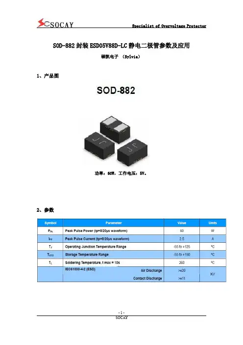
SOD-882封装ESD05V88D-LC静电二极管型号参数及应用
- 格式:pdf
- 大小:371.55 KB
- 文档页数:5

静电保护二极管符号静电保护二极管(ESD protection diode)是一种专门用于保护电子设备或电路元件免受静电放电(ESD)损害的电子元件。
在现代电子技术中,静电放电是一个普遍存在的问题,它可能导致设备故障、数据丢失和设备寿命缩短。
因此,静电保护二极管的使用变得越来越重要。
静电保护二极管符号是用来表示这类二极管的一种标识。
它主要包括两个部分:符号本身和对应的型号。
符号本身通常为一个简化的小图形,表示二极管的类型和功能。
型号则包括制造商名称、器件类型和额定电压等参数。
例如,常见的静电保护二极管符号有TVS(Transient Voltage Suppressor,瞬态电压抑制器)和DIODE(二极管)等。
静电保护二极管符号主要分为以下几类:S二极管:TVS二极管是一种快速响应的瞬态电压抑制器,能有效地抑制电路中的瞬态电压。
它主要用于保护敏感器件,如集成电路、传感器和MOSFET等。
2.压敏电阻二极管:压敏电阻二极管是一种具有特殊电阻-电压曲线的二极管,能在一定电压范围内限制电流。
它主要用于低电压、高频率电路的保护。
3.双向二极管:双向二极管具有正反两个方向的导通特性,可用于防止静电放电引起的电流流动。
它主要用于双向保护的电路。
在选择和使用静电保护二极管符号时,应注意以下几点:1.根据被保护器件的电压、电流和频率特性选择合适的静电保护二极管。
2.确保静电保护二极管的额定电压大于被保护电路的最大工作电压。
3.考虑静电保护二极管的响应速度和钳位电压,以保证其在抑制瞬态电压时能迅速发挥作用。
4.注意静电保护二极管的封装和尺寸,确保其与电路板和被保护器件的兼容性。
总之,静电保护二极管符号是电子电路中不可或缺的一部分。
了解其定义、分类和应用,有助于我们更好地保护电子设备和电路元件,延长设备使用寿命,确保数据安全。
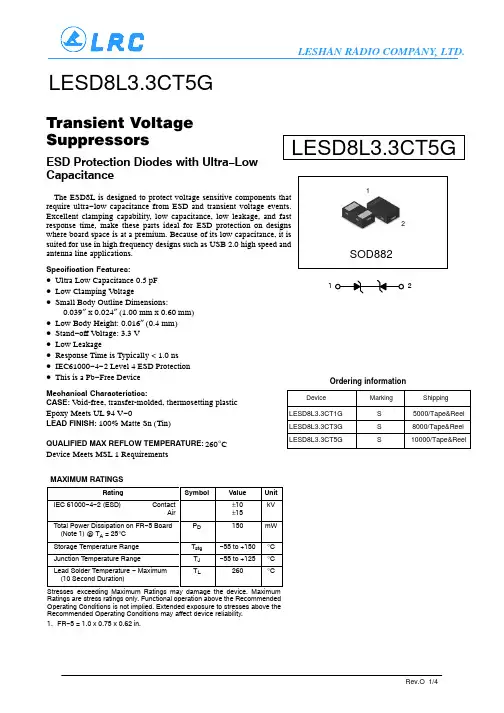
LESD8L3.3CT5GTransient Voltage SuppressorsESD Protection Diodes with Ultra −Low CapacitanceThe ESD8L is designed to protect voltage sensitive components that require ultra −low capacitance from ESD and transient voltage events.Excellent clamping capability, low capacitance, low leakage, and fast response time, make these parts ideal for ESD protection on designs where board space is at a premium. Because of its low capacitance, it is suited for use in high frequency designs such as USB 2.0 high speed and antenna line applications.Specification Features:•Ultra Low Capacitance 0.5 pF •Low Clamping V oltage•Small Body Outline Dimensions:0.039″ x 0.024″(1.00 mm x 0.60 mm)•Low Body Height: 0.016″ (0.4 mm)•Stand −off V oltage: 3.3 V •Low Leakage•Response Time is Typically < 1.0 ns •IEC61000−4−2 Level 4 ESD Protection •This is a Pb −Free DeviceMechanical Characteristics:CASE: V oid-free, transfer-molded, thermosetting plasticEpoxy Meets UL 94 V −0LEAD FINISH: 100% Matte Sn (Tin)QUALIFIED MAX REFLOW TEMPERATURE: Device Meets MSL 1 RequirementsMAXIMUM RATINGSRatingSymbolValue Unit IEC 61000−4−2 (ESD)ContactAir±10±15kV Total Power Dissipation on FR −5 Board (Note 1) @ T A = 25°C °P D°150mW Storage Temperature Range T stg −55 to +150°C Junction Temperature Range T J −55 to +125°C Lead Solder Temperature − Maximum (10 Second Duration)T L 260°CStresses exceeding Maximum Ratings may damage the device. Maximum Ratings are stress ratings only. Functional operation above the Recommended Operating Conditions is not implied. Extended exposure to stresses above the Recommended Operating Conditions may affect device reliability.1.FR −5 = 1.0 x 0.75 x 0.62 in.260°CLESD8L3.3CT5G12SOD88212Ordering informationLESD8L3.3CT5GELECTRICAL CHARACTERISTICS (T A = 25°C unless otherwise noted, V F = 1.0 V Max. @ I F = 10 mA for all types)Device Device MarkingV RWM (V)I R (m A)@ V RWM V BR (V) @ I T (Note 2)I T C (pF)V C (V)@ I PP = 1 A (Note 3)V CMax Max Min mA Typ Max Max Per IEC61000−4−2(Note 4)LESD8L3.3CT5GS3.31.04.81.00.50.910Figures 1 and 2See Below2.V BR is measured with a pulse test current I T at an ambient temperature of 25°C.3.Surge current waveform per Figure 5.4.For test procedure see Figures 3 and 4 and Application Note AND8307/D.ELECTRICAL CHARACTERISTICS(T A = 25°C unless otherwise noted)Symbol ParameterI PP Maximum Reverse Peak Pulse Current V C Clamping Voltage @ I PP V RWM Working Peak Reverse VoltageI R Maximum Reverse Leakage Current @ VRWM V BR Breakdown Voltage @ I T I T Test Current I F Forward Current V F Forward Voltage @ I F P pk Peak Power DissipationCCapacitance @ V R = 0 and f = 1.0 MHz*See Application Note AND8308/D for detailed explanations of datasheet parameters.Figure 1. ESD Clamping Voltage Screenshot Positive 8 kV Contact per IEC61000−4−2Figure 2. ESD Clamping Voltage Screenshot Negative 8 kV Contact per IEC61000−4−2IEC 61000−4−2 Spec.LevelTestVoltage(kV)First PeakCurrent(A)Current at30 ns (A)Current at60 ns (A)127.542 241584 3622.5126 4830168LESHAN RADIO COMPANY, LTD.LESD8L3.3CT5GSOD882DIMENSION OUTLINE:Unit:mm。
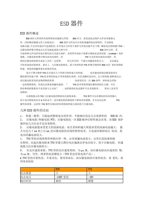
ESD器件ESD器件概述ESD保护元件的作用是转移来自敏感元件的ESD应力,使电流流过保护元件而非敏感元件,同时维持敏感元件上的低电压;ESD保护元件还应具有低泄漏和低电容特性,不会降低电路功能;不会对高速信号造成损害,在多重应力作用下保护元件的功能不会下降。
瞬态电压抑制器(TVS)、压敏电阻和聚合物是近几年发展起来的几种专用ESD呆护元件。
其中前两种元件均采用电压钳位的方式进行保护,采用带导电粒子的聚合物则是采用消弧(crowbar)保护策略。
压敏电阻和聚合物支持双向保护,但TVS可支持单向或双向保护。
传统的压敏电阻虽然在成本上具有一定优势,但它存在的一个最大问题是体积太大,无法满足手持设备的封装要求。
事实上,与压敏电阻相比,基于硅材料的TVS和聚合物材料ESD具有更好的钳制性能、更低的泄漏和更长的使用寿命。
高分子聚合物和TVS在多重应力下仍然可保持强大的性能,而压敏电阻则会随着使用次数的增多性能下降。
TVS技术利用的是半导体的钳位原理,在经受瞬时高压时,会立即将能量释放出去,而压敏电阻采用的是物理吸收原理,因此每经过一次 ESD事件,材料就会受到一定的物理损伤,形成无法恢复的漏电通道。
“TVS技术的原理就好像传统的打太极,可以轻松释放掉能量而不是直接与之对抗”。
这样做的好处是器件不会受到损害,基本上没有寿命限制。
从现场展示的TVS与压敏电阻的钳制电压曲线来看,TVS器件可以在极短时间内将输入的大电压钳制到5至6伏的水平,而压敏电阻的曲线则下降得非常缓慢,并且无法达到TVS器件的效果。
这表明 TVS器件在响应时间和钳制性能方面均优于压敏电阻。
几种ESD器件的比较1、普通二极管,只能起到箝制电压的作用,不能响应高达几百兆频率的ESD脉冲。
2、压敏电阻/热敏电阻/PTC,压敏电阻抗一次ESD脉冲后特性就会改变,而ESD 保护器件抗几万次也不会改变特性。
3、压敏电阻能承受更大的浪涌电流,而且其体积越大所能承受的浪涌电流越大,最大可达几十kA到上百kA;但压敏电阻的非线性特性较差,大电流时限制电压较高,低电压时漏电流较大。
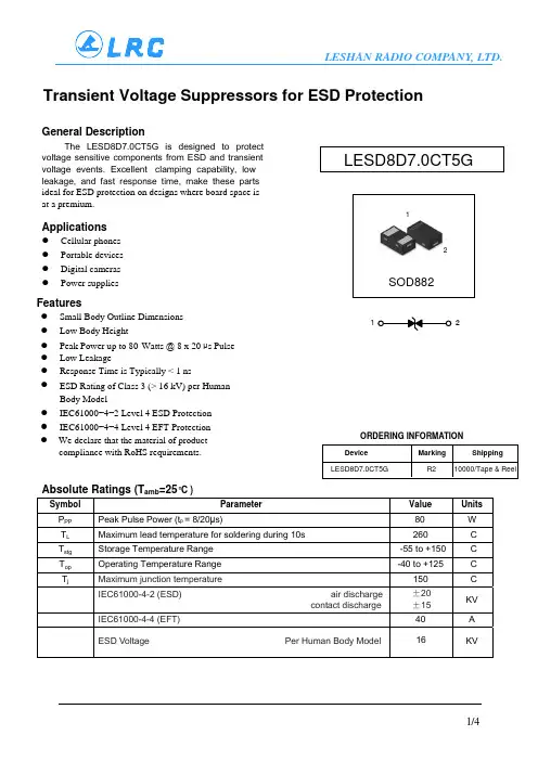
Transient Voltage Suppressors for ESD ProtectionGeneral DescriptionThe LESD8D7.0CT5G is designed to protect voltage sensitive components from ESD and transient voltage events. Excellent clamping capability, low leakage, and fast response time, make these parts ideal for ESD protection on designs where board space isApplicationsFeatureszSmall Body Outline Dimensions z Low Body Heightz z Low Leakage z Response Time is Typically < 1 nsz ESD Rating of Class 3 (> 16 kV) per HumanBody Modelz IEC61000−4−2 Level 4 ESD Protection z IEC61000−4−4 Level 4 EFT Protection z Cellular phones z Portable devices z Digital cameras zPower suppliesAbsolute Ratings (T amb =25°C )SymbolParameterValueUnitsP PP Peak Pulse Power (tp = 8/20μs)80 WT L Maximum lead temperature for soldering during 10s 260 °C T stg Storage Temperature Range -55 to +150 °C T op Operating Temperature Range-40 to +125°CT jMaximum junction temperature 150 °CIEC61000-4-2 (ESD) air dischargecontact discharge ±20±15 KV IEC61000-4-4 (EFT)40 AESD Voltage Per Human Body Model16KVLESHAN RADIO COMPANY, LTD.We declare that the material of product zDevice Marking Shipping ORDERING INFORMATIONat a premium.LESD8D7.0CT5GLESD8D7.0CT5GR2 10000/Tape & ReelSOD8821212Peak Power up to 80 compliance with RoHS req uirements.Watts @ 8 x 20 s Pulse μElectrical ParameterSymbol ParameterI PP Maximum Reverse Peak Pulse CurrentV C Clamping Voltage @ I PPV RWM Working Peak Reverse VoltageI R Maximum Reverse Leakage Current @ V RWMI T Test CurrentV BR Breakdown Voltage @ I TI F Forward CurrentV F Forward Voltage @ I FElectrical Characteristics Ratings at 25°C ambient temperature unless otherwise specified.VF = 0.9V at IF = 10mAV RWM (V)I R(uA)@ V RWMV BR (V)@ I T(Note 1)I TV C (V)@ I PP=3 A*V C (V)@ Max I PP*I PP(A)*P PK(W)*C(pF)DeviceMax Max Min mA Typ Max Max Max Typ LESD8D7.0CT5G 7.0 1.07.2 1.0131658016*Surge current waveform per Figure 1.1. V BR is measured with a pluse test current I T at an ambient temperature of 25℃.LESD8D7.0CT5GFig1. Pulse WaveformFig3.Power DeratingApplication NoteElectrostatic discharge (ESD) is a major cause of failure in electronic systems. Transient V oltage Suppressors (TVS) are an ideal choice for ESD protection. They are capable of clamping the incoming transient to a low enough level such that damage to the protected semiconductor is prevented.Surface mount TVS offer the best choice for minimal lead inductance. They serve as parallel protection elements, connected between the signal line to ground. As the transient rises above the operating voltage of thedevice, the TVS becomes a low impedance path diverting the transient current to ground.is the ideal board evel protection of ESD sensitive semiconductor components.The tiny SOD882 package allows design flexibility in the design of high density boards where the space saving is at a premium. This enables to shorten the routing and contributes to hardening againt ESD.The LESD8D7.0CT5G LESD8D7.0CT5GLESD8D7.0CT5G OUTLINE AND DIMENSIONSSOLDERING FOOTPRINT。