74HC74
- 格式:pdf
- 大小:153.46 KB
- 文档页数:2
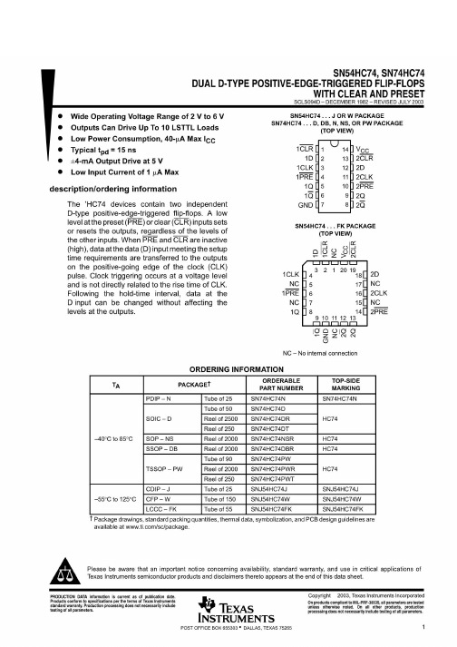
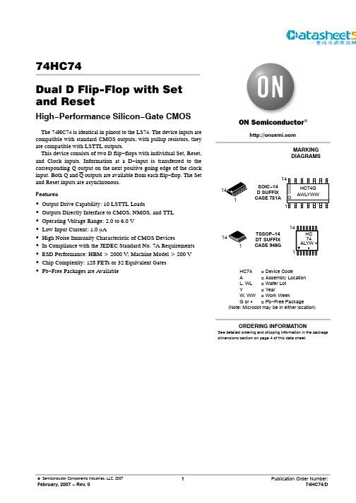
74HC74Dual D Flip−Flop with Set and ResetHigh −Performance Silicon −Gate CMOSThe 74HC74 is identical in pinout to the LS74. The device inputs arecompatible with standard CMOS outputs; with pullup resistors, theyare compatible with LSTTL outputs.This device consists of two D flip −flops with individual Set, Reset,and Clock inputs. Information at a D −input is transferred to thecorresponding Q output on the next positive going edge of the clockinput. Both Q and Q outputs are available from each flip −flop. The Setand Reset inputs are asynchronous.Features •Output Drive Capability: 10 LSTTL Loads •Outputs Directly Interface to CMOS, NMOS, and TTL •Operating V oltage Range: 2.0 to 6.0 V •Low Input Current: 1.0 m A •High Noise Immunity Characteristic of CMOS Devices •In Compliance with the JEDEC Standard No. 7A Requirements •ESD Performance: HBM > 2000 V; Machine Model > 200 V •Chip Complexity: 128 FETs or 32 Equivalent Gates•Pb −Free Packages are Available MARKING DIAGRAMS HC74= Device CodeA = Assembly LocationL, WL = Wafer LotY = YearW, WW = Work WeekG or G = Pb −Free PackageTSSOP −14DT SUFFIX CASE 948GSOIC −14D SUFFIX CASE 751AHC 74ALYW G G 114See detailed ordering and shipping information in the packagedimensions section on page 4 of this data sheet.ORDERING INFORMATION(Note: Microdot may be in either location)RESET 1DATA 1CLOCK 1SET 1RESET 2DATA 2CLOCK 2SET 2Q1Q1Q2Q2PIN 14 = V CC PIN 7 = GND FUNCTION TABLEstates are unpredictable if Set and Reset go high simultaneously.LOGIC DIAGRAM PIN ASSIGNMENTSET 1CLOCK 1DATA 1RESET 1SET 2CLOCK 2DATA 2RESET 2V CC Q2Q2GND Q1Q1MAXIMUM RATINGSSymbolParameter Value Unit V CCDC Supply Voltage (Referenced to GND)– 0.5 to + 7.0V V inDC Input Voltage (Referenced to GND)– 0.5 to V CC + 0.5V V outDC Output Voltage (Referenced to GND)– 0.5 to V CC + 0.5V I inDC Input Current, per Pin ±20mA I outDC Output Current, per Pin ±25mA I CCDC Supply Current, V CC and GND Pins ±50mA P DPower Dissipation in Still Air,SOIC Package†TSSOP Package†500450mW T stgStorage Temperature – 65 to + 150_C T L Lead Temperature, 1 mm from Case for 10 Seconds(SOIC or TSSOP Package)260300_C Stresses exceeding Maximum Ratings may damage the device. Maximum Ratings are stress ratings only. Functional operation above the Recommended Operating Conditions is not implied.Extended exposure to stresses above the Recommended Operating Conditions may affect device reliability.†Derating —SOIC Package: – 7 mW/_C from 65_ to 125_CTSSOP Package: − 6.1 mW/_C from 65_ to 125_C For high frequency or heavy load considerations, see Chapter 2 of the ON Semiconductor High −Speed CMOS Data Book (DL129/D).RECOMMENDED OPERATING CONDITIONSSymbolParameter Min Max Unit V CCDC Supply Voltage (Referenced to GND) 2.0 6.0V V in , V outDC Input Voltage, Output Voltage (Referenced to GND)0V CC V T AOperating Temperature, All Package Types – 55+ 125_C t r , t f Input Rise and Fall TimeV CC = 2.0 V(Figures 1, 2, 3)V CC = 3.0 VV CC = 4.5 VV CC = 6.0 V 00001000600500400nsThis device contains protection circuitry to guard against damage due to high static voltages or electric fields. However, precautions must be taken to avoid applications of any voltage higher than maximum rated voltages to this high −impedance cir-cuit. For proper operation, V in and V out should be constrained to the range GND v (V in or V out ) v V CC .Unused inputs must always be tied to an appropriate logic voltage level (e.g., either GND or V CC ).Unused outputs must be left open.DC ELECTRICAL CHARACTERISTICS (Voltages Referenced to GND)Symbol Parameter Test Conditions V CC(V)Guaranteed LimitUnit – 55 to25_C v85_C v 125_CV IH Minimum High−Level Input Voltage V out = 0.1 V or V CC – 0.1 V|I out| v 20 m A2.03.04.56.01.52.13.154.21.52.13.154.21.52.13.154.2VV IL Maximum Low−Level Input Voltage V out = 0.1 V or V CC – 0.1 V|I out| v 20 m A2.03.04.56.00.50.91.351.80.50.91.351.80.50.91.351.8VV OH Minimum High−Level Output Voltage V in = V IH or V IL|I out| v 20 m A2.04.56.01.94.45.91.94.45.91.94.45.9VV in = V IH or V IL|I out| v 2.4 mA|I out| v 4.0 mA|I out| v 5.2 mA3.04.56.02.483.985.482.343.845.342.23.75.2V OL Maximum Low−Level Output Voltage V in = V IH or V IL|I out| v 20 m A2.04.56.00.10.10.10.10.10.10.10.10.1V V in = V IHor V IL|I out| v 2.4 mA|I out| v 4.0 mA|I out| v 5.2 mA3.04.56.00.260.260.260.330.330.330.40.40.4I in Maximum Input Leakage Current V in = V CC or GND 6.0±0.1±1.0±1.0m AI CC Maximum Quiescent SupplyCurrent (per Package)V in = V CC or GNDI out = 0 m A6.0 2.02080m ANOTE:Information on typical parametric values can be found in Chapter 2 of the ON Semiconductor High−Speed CMOS Data Book (DL129/D).AC ELECTRICAL CHARACTERISTICS (C L = 50 pF, Input t r = t f= 6.0 ns)Symbol Parameter V CC(V)Guaranteed LimitUnit – 55 to25_C v85_C v 125_Cf max Maximum Clock Frequency (50% Duty Cycle)(Figures 1 and 4)2.03.04.56.06.01530354.81024284.08.02024MHzt PLH, t PHL Maximum Propagation Delay, Clock to Q or Q(Figures 1 and 4)2.03.04.56.01007520171259025211501203026nst PLH, t PHL Maximum Propagation Delay, Set or Reset to Q or Q(Figures 2 and 4)2.03.04.56.01058021181309526221601303227nst TLH, t THL Maximum Output Transition Time, Any Output(Figures 1 and 4)2.03.04.56.07530151395401916110552219nsC in Maximum Input Capacitance—101010pF NOTE:For propagation delays with loads other than 50 pF, and information on typical parametric values, see Chapter 2 of the ON Semiconductor High−Speed CMOS Data Book (DL129/D).C PD Power Dissipation Capacitance (Per Flip−Flop)*Typical @ 25°C, V CC = 5.0 VpF32*Used to determine the no−load dynamic power consumption: P D = C PD V CC2f + I CC V CC. For load considerations, see Chapter 2 of the ON Semiconductor High−Speed CMOS Data Book (DL129/D).TIMING REQUIREMENTS (Input t r = t f = 6.0 ns)SymbolParameter V CC (V)Guaranteed LimitUnit – 55 to 25_C v 85_C v 125_C t su Minimum Setup Time, Data to Clock(Figure 3) 2.03.04.56.080351614100452017120552420ns t h Minimum Hold Time, Clock to Data(Figure 3) 2.03.04.56.03.03.03.03.0 3.03.03.03.0 3.03.03.03.0ns t rec Minimum Recovery Time, Set or Reset Inactive to Clock (Figure 2) 2.03.04.56.08.08.08.08.08.08.08.08.08.08.08.08.0ns t w Minimum Pulse Width, Clock (Figure 1) 2.03.04.56.0602512107530151390401815ns t w Minimum Pulse Width, Set or Reset (Figure 2) 2.03.04.56.0602512107530151390401815ns t r , t f Maximum Input Rise and Fall Times (Figures 1, 2, 3) 2.03.04.56.0100080050040010008005004001000800500400nsORDERING INFORMATIONDevicePackage Shipping †74HC74DSOIC −1455 Units / Rail 74HC74DGSOIC −14(Pb −Free)74HC74DR2SOIC −142500 / Tape & Reel 74HC74DR2GSOIC −14(Pb −Free)74HC74DTR2TSSOP −14*74HC74DTR2G TSSOP −14*†For information on tape and reel specifications, including part orientation and tape sizes, please refer to our Tape and Reel Packaging Specifications Brochure, BRD8011/D.*This package is inherently Pb −Free.SWITCHING WAVEFORMSSET DATARESETFigure 5. EXPANDED LOGIC DIAGRAMPACKAGE DIMENSIONSSOIC −14CASE 751A −03ISSUE HNOTES:1.DIMENSIONING AND TOLERANCING PER ANSI Y14.5M, 1982.2.CONTROLLING DIMENSION: MILLIMETER.3.DIMENSIONS A AND B DO NOT INCLUDE MOLD PROTRUSION.4.MAXIMUM MOLD PROTRUSION 0.15 (0.006)PER SIDE.5.DIMENSION D DOES NOT INCLUDE DAMBAR PROTRUSION. ALLOWABLE DAMBAR PROTRUSION SHALL BE 0.127(0.005) TOTAL IN EXCESS OF THE D DIMENSION AT MAXIMUM MATERIAL CONDITION.DIM MIN MAX MIN MAX INCHES MILLIMETERS A 8.558.750.3370.344B 3.80 4.000.1500.157C 1.35 1.750.0540.068D 0.350.490.0140.019F 0.40 1.250.0160.049G 1.27 BSC 0.050 BSC J 0.190.250.0080.009K 0.100.250.0040.009M 0 7 0 7 P 5.80 6.200.2280.244R 0.250.500.0100.019____DIMENSIONS: MILLIMETERS*For additional information on our Pb −Free strategy and soldering details, please download the ON Semiconductor Soldering and Mounting Techniques Reference Manual, SOLDERRM/D.PACKAGE DIMENSIONSTSSOP −14CASE 948G −01ISSUE B DIM MIN MAX MIN MAX INCHES MILLIMETERS A 4.90 5.100.1930.200B 4.30 4.500.1690.177C −−− 1.20−−−0.047D 0.050.150.0020.006F 0.500.750.0200.030G 0.65 BSC 0.026 BSC H 0.500.600.0200.024J 0.090.200.0040.008J10.090.160.0040.006K 0.190.300.0070.012K10.190.250.0070.010L 6.40 BSC 0.252 BSC M 0 8 0 8 NOTES:1.DIMENSIONING AND TOLERANCING PER ANSI Y14.5M, 1982.2.CONTROLLING DIMENSION: MILLIMETER.3.DIMENSION A DOES NOT INCLUDE MOLD FLASH, PROTRUSIONS OR GATE BURRS.MOLD FLASH OR GATE BURRS SHALL NOT EXCEED 0.15 (0.006) PER SIDE.4.DIMENSION B DOES NOT INCLUDE INTERLEAD FLASH OR PROTRUSION.INTERLEAD FLASH OR PROTRUSION SHALL NOT EXCEED 0.25 (0.010) PER SIDE.5.DIMENSION K DOES NOT INCLUDE DAMBAR PROTRUSION. ALLOWABLE DAMBAR PROTRUSION SHALL BE 0.08(0.003) TOTAL IN EXCESS OF THE K DIMENSION AT MAXIMUM MATERIAL CONDITION.6.TERMINAL NUMBERS ARE SHOWN FOR REFERENCE ONLY .7.DIMENSION A AND B ARE TO BE DETERMINED AT DATUM PLANE −W −.____14X REF K14X 0.360.65PITCHSOLDERING FOOTPRINT**For additional information on our Pb −Free strategy and soldering details, please download the ON Semiconductor Soldering and Mounting Techniques Reference Manual, SOLDERRM/D.ON Semiconductor and are registered trademarks of Semiconductor Components Industries, LLC (SCILLC). SCILLC reserves the right to make changes without further notice to any products herein. SCILLC makes no warranty, representation or guarantee regarding the suitability of its products for any particular purpose, nor does SCILLC assume any liability arising out of the application or use of any product or circuit, and specifically disclaims any and all liability, including without limitation special, consequential or incidental damages.“Typical” parameters which may be provided in SCILLC data sheets and/or specifications can and do vary in different applications and actual performance may vary over time. All operating parameters, including “Typicals” must be validated for each customer application by customer’s technical experts. SCILLC does not convey any license under its patent rights nor the rights of others. SCILLC products are not designed, intended, or authorized for use as components in systems intended for surgical implant into the body, or other applications intended to support or sustain life, or for any other application in which the failure of the SCILLC product could create a situation where personal injury or death may occur. Should Buyer purchase or use SCILLC products for any such unintended or unauthorized application, Buyer shall indemnify and hold SCILLC and its officers, employees, subsidiaries, affiliates, and distributors harmless against all claims, costs, damages, and expenses, and reasonable attorney fees arising out of, directly or indirectly, any claim of personal injury or death associated with such unintended or unauthorized use, even if such claim alleges that SCILLC was negligent regarding the design or manufacture of the part. SCILLC is an Equal Opportunity/Affirmative Action Employer. This literature is subject to all applicable copyright laws and is not for resale in any manner.PUBLICATION ORDERING INFORMATION。


74HC/LS/HCT/F系列芯片的区别:1、 LS是低功耗肖特基,HC是高速COMS。
LS的速度比HC略快。
HCT 输入输出与LS兼容,但是功耗低;F是高速肖特基电路;2、 LS是TTL电平,HC是COMS电平。
3、 LS输入开路为高电平,HC输入不允许开路, hc 一般都要求有上下拉电阻来确定输入端无效时的电平。
LS 却没有这个要求4、 LS输出下拉强上拉弱,HC上拉下拉相同。
5、工作电压不同,LS只能用5V,而HC一般为2V到6V;而HCT的工作电压一般为4.5V~5.5V。
6、电平不同。
LS是TTL电平,其低电平和高电平分别为0.8和V2.4,而CMOS在工作电压为5V时分别为0.3V和3.6V,所以CMOS 可以驱动TTL,但反过来是不行的7、驱动能力不同,LS一般高电平的驱动能力为5mA,低电平为20mA;而CMOS的高低电平均为5mA;8、 CMOS器件抗静电能力差,易发生栓锁问题,所以CMOS的输入脚不能直接接电源。
74系列集成电路大致可分为6大类:.74××(标准型);.74LS××(低功耗肖特基);.74S××(肖特基);.74ALS××(先进低功耗肖特基);.74AS××(先进肖特基);.74F××(高速)。
近年来还出现了高速CMOS电路的74系列,该系列可分为3大类:.HC为COMS工作电平;.HCT为TTL工作电平,可与74LS系列互换使用;.HCU适用于无缓冲级的CMOS电路。
这9种74系列产品,只要后边的标号相同,其逻辑功能和管脚排列就相同。
根据不同的条件和要求可选择不同类型的74系列产品,比如电路的供电电压为3V就应选择74HC系列的产品系列电平典型传输延迟ns 最大驱动电流(-Ioh/Lol)mAAHC CMOS 8.5 -8/8AHCT COMS/TTL 8.5 -8/8HC COMS 25 -8/8HCT COMS/TTL 25 -8/8ACT COMS/TTL 10 -24/24F TTL 6.5 -15/64ALS TTL 10 -15/64LS TTL 18 -15/24注:同型号的74系列、74HC系列、74LS系列芯片,逻辑功能上是一样的。
PACKAGING INFORMATIONOrderable Device Status(1)PackageType PackageDrawingPins PackageQtyEco Plan(2)Lead/Ball Finish MSL Peak Temp(3)5962-8405601VCA ACTIVE CDIP J141None Call TI Level-NC-NC-NC 5962-8405601VDA ACTIVE CFP W141None Call TI Level-NC-NC-NC 84056012A ACTIVE LCCC FK201None Call TI Level-NC-NC-NC 8405601CA ACTIVE CDIP J141None Call TI Level-NC-NC-NC 8405601DA ACTIVE CFP W141None Call TI Level-NC-NC-NC JM38510/65302B2A ACTIVE LCCC FK201None Call TI Level-NC-NC-NC JM38510/65302BCA ACTIVE CDIP J141None Call TI Level-NC-NC-NC JM38510/65302BDA ACTIVE CFP W141None Call TI Level-NC-NC-NC SN54HC74J ACTIVE CDIP J141None Call TI Level-NC-NC-NC SN74HC74ADBLE OBSOLETE SSOP DB14None Call TI Call TISN74HC74D ACTIVE SOIC D1450Pb-Free(RoHS)CU NIPDAU Level-2-260C-1YEAR/Level-1-235C-UNLIMSN74HC74DBLE OBSOLETE SSOP DB14None Call TI Call TISN74HC74DBR ACTIVE SSOP DB142000Pb-Free(RoHS)CU NIPDAU Level-2-260C-1YEAR/Level-1-235C-UNLIMSN74HC74DR ACTIVE SOIC D142500Green(RoHS&no Sb/Br)CU NIPDAU Level-1-260C-UNLIMSN74HC74DT ACTIVE SOIC D14250Pb-Free(RoHS)CU NIPDAU Level-2-260C-1YEAR/Level-1-235C-UNLIMSN74HC74N ACTIVE PDIP N1425Pb-Free(RoHS)CU NIPDAU Level-NC-NC-NC SN74HC74N3OBSOLETE PDIP N14None Call TI Call TISN74HC74NSR ACTIVE SO NS142000Pb-Free(RoHS)CU NIPDAU Level-2-260C-1YEAR/Level-1-235C-UNLIMSN74HC74PW ACTIVE TSSOP PW1490Pb-Free(RoHS)CU NIPDAU Level-1-250C-UNLIMSN74HC74PWLE OBSOLETE TSSOP PW14None Call TI Call TISN74HC74PWR ACTIVE TSSOP PW142000Pb-Free(RoHS)CU NIPDAU Level-1-250C-UNLIMSN74HC74PWT ACTIVE TSSOP PW14250Pb-Free(RoHS)CU NIPDAU Level-1-250C-UNLIM SNJ54HC74FK ACTIVE LCCC FK201None Call TI Level-NC-NC-NC SNJ54HC74J ACTIVE CDIP J141None Call TI Level-NC-NC-NC SNJ54HC74W ACTIVE CFP W141None Call TI Level-NC-NC-NC (1)The marketing status values are defined as follows:ACTIVE:Product device recommended for new designs.LIFEBUY:TI has announced that the device will be discontinued,and a lifetime-buy period is in effect.NRND:Not recommended for new designs.Device is in production to support existing customers,but TI does not recommend using this part in a new design.PREVIEW:Device has been announced but is not in production.Samples may or may not be available.OBSOLETE:TI has discontinued the production of the device.(2)Eco Plan-May not be currently available-please check /productcontent for the latest availability information and additional product content details.None:Not yet available Lead(Pb-Free).Pb-Free(RoHS):TI's terms"Lead-Free"or"Pb-Free"mean semiconductor products that are compatible with the current RoHS requirements for all6substances,including the requirement that lead not exceed0.1%by weight in homogeneous materials.Where designed to be soldered at high temperatures,TI Pb-Free products are suitable for use in specified lead-free processes.Green(RoHS&no Sb/Br):TI defines"Green"to mean"Pb-Free"and in addition,uses package materials that do not contain halogens, including bromine(Br)or antimony(Sb)above0.1%of total product weight.(3)MSL,Peak Temp.--The Moisture Sensitivity Level rating according to the JEDECindustry standard classifications,and peak solder temperature.Important Information and Disclaimer:The information provided on this page represents TI's knowledge and belief as of the date that it is provided.TI bases its knowledge and belief on information provided by third parties,and makes no representation or warranty as to the accuracy of such information.Efforts are underway to better integrate information from third parties.TI has taken and continues to take reasonable steps to provide representative and accurate information but may not have conducted destructive testing or chemical analysis on incoming materials and chemicals.TI and TI suppliers consider certain information to be proprietary,and thus CAS numbers and other limited information may not be available for release.In no event shall TI's liability arising out of such information exceed the total purchase price of the TI part(s)at issue in this document sold by TI to Customer on an annual basis.元器件交易网IMPORTANT NOTICETexas Instruments Incorporated and its subsidiaries (TI) reserve the right to make corrections, modifications,enhancements, improvements, and other changes to its products and services at any time and to discontinueany product or service without notice. Customers should obtain the latest relevant information before placingorders and should verify that such information is current and complete. All products are sold subject to TI’s termsand conditions of sale supplied at the time of order acknowledgment.TI warrants performance of its hardware products to the specifications applicable at the time of sale inaccordance with TI’s standard warranty. T esting and other quality control techniques are used to the extent TIdeems necessary to support this warranty. Except where mandated by government requirements, testing of allparameters of each product is not necessarily performed.TI assumes no liability for applications assistance or customer product design. Customers are responsible fortheir products and applications using TI components. T o minimize the risks associated with customer productsand applications, customers should provide adequate design and operating safeguards.TI does not warrant or represent that any license, either express or implied, is granted under any TI patent right,copyright, mask work right, or other TI intellectual property right relating to any combination, machine, or processin which TI products or services are used. Information published by TI regarding third-party products or servicesdoes not constitute a license from TI to use such products or services or a warranty or endorsement thereof.Use of such information may require a license from a third party under the patents or other intellectual propertyof the third party, or a license from TI under the patents or other intellectual property of TI.Reproduction of information in TI data books or data sheets is permissible only if reproduction is withoutalteration and is accompanied by all associated warranties, conditions, limitations, and notices. Reproductionof this information with alteration is an unfair and deceptive business practice. TI is not responsible or liable forsuch altered documentation.Resale of TI products or services with statements different from or beyond the parameters stated by TI for thatproduct or service voids all express and any implied warranties for the associated TI product or service andis an unfair and deceptive business practice. TI is not responsible or liable for any such statements.Following are URLs where you can obtain information on other Texas Instruments products and applicationsolutions:Products ApplicationsAmplifiers Audio /audioData Converters Automotive /automotiveDSP Broadband /broadbandInterface Digital Control /digitalcontrolLogic Military /militaryPower Mgmt Optical Networking /opticalnetworkMicrocontrollers Security /securityTelephony /telephonyVideo & Imaging /videoWireless /wirelessMailing Address:Texas InstrumentsPost Office Box 655303 Dallas, Texas 75265Copyright 2005, Texas Instruments Incorporated。
74HC74管脚排列
74HC74 概述
74HC74是一款高速CMOS器件,74HC74引脚兼容低功耗肖特基TTL (LSTTL)系列。
74HC74遵循JEDEC标准no.7A。
74HC74是双路D 型上升沿触发器,带独立的数据(D)输入、时钟(CP)输入、设置(SD)和复位(RD)输入、以及互补的Q和Q输出。
设置和复位为异步低电平有效,且不依赖于时钟输入。
74HC74数据输入口的信息在时钟脉冲的上升沿传输到Q口。
为了获得预想中的结果,D输入必须在时钟脉冲上升沿来临之前,保持稳定一段就绪时间。
74HC74时钟输入的施密特触发功能使得电路对于缓慢的脉冲上升和下降具备更高的容差性。
74HC74 特性
工作电压范围:2.0~6.0 V
对称输出阻抗
高抗扰
低功耗
ESD保护
HBM EIA/JESD22-A114-A超过2000 V
MM EIA/JESD22-A115-A超过200 V
74HC74 参数
74HC74 基本参数
电压 2.0~6.0V
驱动电流+/-5.2 mA
传输延迟14 ns@5V
74HC74 其他特性
逻辑电平CMOS
功耗考量低功耗或电池供电应用74HC74 封装与引脚
SO14, SSOP14, DIP14, TSSOP14。
74HC系列芯⽚资料74HC00 四 2 输⼊与⾮门国际通⽤符号54/7400 , 54/74H00 , 54L 00 , 54/74S00 , 54/74LS00 , 54/74ALS00 , 54/ 74F 00 , 54/74HC00 , 54/ 74AC 00 ,54/74HCT00 , 54/74ACT00 , 54/74AHC00 , 54/74AHCT00 , 74LV00 ,74LVC00。
74HC02 四 2 输⼊或⾮门国际通⽤符号54/7402 , 54L 02 , 54/74S02 , 54/74LS02 , 54/74AS02 , 54/74ALS02 , 54/ 74F 02 , 54/74HC02 , 74AC 02 ,54/74HCT02 , 54/74ACT02 , 54/74AHC02 , 54/AHCT02 , 74LV02 ,74LVC02。
74HC04 六反相器国际通⽤符号54/7404 , 54L 04 , 54/74H04 , 54/74S04 , 54/74LS04 , 54/74AS04 , 54/74ALS04 ,54/ 74F 04 , 54/74HCU04 ,54/74HC04 , 54/ 74AC 04 , 54/74HCT04 , 54/74ACT04 ,54/74AHC04 , 54/74AHCT04 , 74LV04 , 74LVC04 ,54/74AHCU04 , 74LVU04 , 74LVCU04。
74HC08 四 2 输⼊与门国际通⽤符号54/7408 , 54/74S08 , 54/74LS08 , 54/74AS08 , 54/74ALS08 , 54/ 74F 08 , 54/74HC08 ,54/74HCT08 , 54/ 74AC 08 , 54/74ACT08 , 54/74AHC08 , 54/74AHCT08 , 74LV08 , 74LVC08。