MAX6366HKA23+T中文资料
- 格式:pdf
- 大小:538.29 KB
- 文档页数:15

W6360Dark GrayWCDMA / GSMCTW6360GYCool screen, hot newspowered by AndroidWatch live sports games and the latest news while on the move with the cool Philips W6360 smartphone. With its 4.3" capacitive touch screen, ISDB-T mobile TV, Android 4.1 and 1.2 GHz dual core processor, you’ll be first in the know.Fast, simple and easySpeedy data with HSDPA and HSUPACreate a personal WiFi hotspot and get connected on the goGo online anywhere with plug and play USB modemBrilliantly smartSlick mobile performance with 1.2GHz dual core processor4.3" capacitive touch screen for intuitive navigationWatch live shows on the go with ISDB-T mobile TVAndroid 4.1Extras in life5 megapixel autofocus camera with flashInternet access on the move over WLANConvenienceButtons and controls: Power On/Off, Side keysCall Management: Call Forwarding, Call on Hold, Call Time, Call Waiting*, Caller ID*,Emergency Call, Microphone mute, Missed Calls, Received Calls, Firewall, Video chatClock/Version: Analogue, Digital, International clock Ease of Navigation: Touch panelEase of Use: Graphical User Interface, Hands free mode, Hot Keys, In-flight mode, Keypad Lock, Softkeys, Vibra AlertGames and applications: Alarm Clock, Calculator, Calendar, Document Viewer, Motion sensor, Agenda, File Manager, Photo Editor, Widget Language available: UI: English, Spanish Operating System: Android 4.1Personal Info Management: Time Zone, Smart Phonebook, International clock, Task list, Quick Note Personalisation/Customization: Downloadable Animated GIF, Downloadable Picture, Downloadable Ringtones, Wallpaper, Ringtones, Downloadable wallpaper Text input: Smart predictive input Vibrator Volume control GPS Built-in GPS Supports A-GPS Connectivity Headset: Via 3.5mm jack connector Modem Capabilities: GPRS, SMS, EDGE, HSPA DL 7.2Mbps, HSUPA 5.76Mbps, WCDMA PC Link: USB 2.0Serial connections: USB-Jack cable Wireless connections: Wi-Fi, Bluetooth Bluetooth profiles: A2DP, AVRCP, GAP, GAVDP, GOEP, HFP, HSP, OPP Bluetooth version: 3.0Accessories Standard Package Includes: Battery, Charger, Handset, User Manual, USB data cable Batteries: 2000mAh PowerBattery Capacity: 2000 mAh Battery Type: Lithium-ion Standby time: GSM up to 500 hours,WCDMA up to 400 hours Talk time: GSM up to 13 hours,WCDMA up to 8 hours Processor 1.2 GHz Dual Core Processor OS Android: Android 4.1Smartphone CTW6360GY/55SpecificationsNetwork Features GPRS (Rx+Tx): Class 12, class B and C GSM band: 850, 900, 1800, 1900 MHz Messaging: E-mail, MMS,Multimedia Message Service, SMS (Short Message Service)Services: SIM Toolkit / Release 99, WAP 2.0Voice Codec: FR/EFR/AMR/HREDGE 3G: WCDMA WCDMA band: 850MHz, 1900MHz WLAN Dimensions Antenna: Integrated Form Factor: Candy bar Handset color: Gray Picture/Display Main Display Colors: 16M Main Display Resolution: 480x800 pixel Main Display Technology: TFT Touch panel Touch-sensitive screen: Touch Screen Capacity touch panel Still Picture Capturing Camera: Integrated Flash: built-in Integrated flash Preview frame rate: 30 frames/second Picture file format: JPEG Picture resolution: 5M (2592x1944), 2M (1600x1200), 3M (2048x1536)White balance: Automatic, Cloudy,Incandescent, Fluorescent, Daylight Picture quality: Normal, Fine, SuperfineStill Picture PlaybackPicture Compression Format: BMP, GIF, GIF (87a & 89a), JPEG, WBMPPicture Enhancement: Create albums, Editphotos (colors, filters), Flip photos, Frames &Icons, Rotate, Tag it, Picture editor Rotation: 90 degree steps Slide show Video CapturingVideo format: H.263, H.264, mp4Video resolution: QVGA, QCIF, VGAVideo PlaybackCompression formats: H.263, H.264Frame rate (fps): 30Resolution (pxl): 176x144, 352x288, 640x480,800x480, 854x480, 1280x720, 720x480Video Recording Compression formats: MPEG4, H.263, H.264Frame rate: 30 fps Resolution (pxl): 640x480, 800x480,854x480, 1280x720Max resolution: HD(720p) pixel Audio CapturingVoice recording: Yes, AMRAudio Playback Audio supported formats: AAC, AAC+, Midi,MP3, WAV Sound Ringers: MP3 ringer, AMR ringer Storage MediaBuilt-in memory (RAM): 512 MB Memory Card Types: Micro SDMemory management: Memory status,Dynamic memory allocation User memory: 942 MBMaximum memory card capacity: 32 GB* Specifications indicated are based on an initial full battery charge tested in a laboratory with Bluetooth and WiFi switched off. Actual performance will depend on network service provider and usage.* MicroSD memory card is not included.* GPS/AGPS connections are subject to local network and data service availabity and providers may charge users additional fees. Connection times may also be affected by external factors, such as surrounding environment, weather, etc* Availability of certain features is subject to valid service subscription from your network operator.© 2019 Koninklijke Philips N.V .All Rights reserved.Specifications are subject to change without notice. Trademarks are the property of Koninklijke Philips N.V . or their respective owners.Issue date 2019‑10‑23Version: 3.0.112 NC: 8670 001 01439EAN: 87 12581 68186 。

Series 6, Built-in oven, 60 x 60 cm, Stainless steelHBA5780S6BIncluded accessories2 x combination grid, 1 x universal panOptional accessoriesHEZ317000 Pizza pan, enamelled, HEZ327000 Pizza stone,HEZ531000 Baking tray, enamelled, HEZ531010 Baking tray,non-stick ceramic coated, HEZ532000 Multipurpose pan, enamelled, HEZ532010 Universal pan, non-stick ceramic coated, HEZ5380001fold telescopic rail, level independent, HEZ629070 Air Fry & Grill tray, HEZ634000 Baking and roasting grid (standard), HEZ638000 Full ext rails, level independent, HEZ660050 Cover Strip, HEZ664000 Baking and roasting grid (steam), HEZ915003 Glass roasting dish, 5,4 L The built-in oven with AutoPilot: automatically prepares perfect dishes.• AutoPilot 30: Perfectly cooks dishes thanks to 30 pre-set automatic programmes.• White LCD display control: easy-to-use thanks to direct access to additional functions, temperature recommendation and temperature indication.• Pop-out controls: Make the front of the oven easy to clean and give it a sleek look.• Pyrolytic self-cleaning: Automatically cleans the oven, just wipe out the ash.• 1-stage telescopic rails, level independent: can be placed in any baking level.Technical DataInstallation type: ......................................................................Built-in Integrated Cleaning system: ..................................................Pyrolytic Min. required niche size for installation (HxWxD): 585-595 x 560-568 x 550 mmDimensions: ........................................................595 x 594 x 548 mm Dimensions of the packed product (HxWxD): .....675 x 690 x 660 mm Control Panel Material: ................................................Stainless steel Door Material: ............................................................................Glass Net weight: ..............................................................................37.9 kg Usable volume of cavity: ...............................................................71 l Cooking method: .......Defrost, Full width grill, Hotair gentle, Hot Air, Conventional heat, Pizza setting, low temperature cooking, Hot air grilling, warmingFirst cavity material: ..................................................................Other Oven control: ......................................................................electronic Number of interior lights: .. (1)Length of electrical supply cord: ..........................................120.0 cm EAN code: (4242005177059)Number of cavities (2010/30/EC): (1)Energy efficiency rating: ....................................................................A Energy consumption per cycle conventional (2010/30/EC): ........0.99 kWh/cycleEnergy consumption per cycle forced air convection (2010/30/EC):0.81 kWh/cycleEnergy efficiency index (2010/30/EC): .....................................95.3 % Connection rating: ..................................................................2990 W Fuse protection: ...........................................................................13 A Voltage: ...............................................................................220-240 V Frequency: ...........................................................................50; 60 Hz Plug type: .....................no plug (electrical connection by electrician) Included accessories: .............2 x combination grid, 1 x universal panSeries 6, Built-in oven, 60 x 60 cm, Stainless steelHBA5780S6BThe built-in oven with AutoPilot: automatically prepares perfect dishes.Design- Rotary dial, Retractable control dials, round- Straight bar handleFeatures- Home Connect ready- Electronic door lock- Control panel lock Automatic safety switch off Residual heat indicator Door contact switch- Digital temperature display with proposal- Heating-up indicator AutoPilot Automatic start- AutoPilot, 30- Integral cooling fan- 5 shelf positions- Electronic clock timer- Interior halogen light, Light on/off when oven door opened/closed Cleaning- Pyrolytic self-cleaning function- Full glass inner doorProgrammes/functions- Oven with 9 PC heating methods: 3D Hotair, conventional top and bottom heat, Hotair grilling, full width variable grill, pizza function, low temperature cooking, defrost, keep warm, Hotair gentle- Fast pre-heating function- Automatic programmesAccessories- 2 x combination grid, 1 x universal pan- 1 set of level independent telescopic rails, Stop function Performance/technical information- Energy efficiency rating (acc. EU Nr. 65/2014): A- Energy consumption per cycle in conventional mode:0.99 kWh- Energy consumption per cycle in fan-forced convection mode:0.81 kWh- Number of cavities: Main cavity Heat source: electrical Cavity volume:71 litre capacity- 120 cm Cable length- Total connected load electric: 2.99 KW- Temperature range 30 °C - 275 °C- Nominal voltage: 220 - 240 V- Appliance dimension (hxwxd): 595 mm x 594 mm x 548 mm- Niche dimension (hxwxd): 585 mm - 595 mm x 560 mm - 568 mm x 550 mm- Please refer to the dimensions provided in the installation manualSeries 6, Built-in oven, 60 x 60 cm,Stainless steel HBA5780S6B。

1 TB、750 GB、500 GB、320 GB、250 GB、160 GB •7200 RPM • SATA 3 Gb/秒,支援 NCQ主要優勢•支援常見的入門級與主流桌上型 PC•提供 160 GB 到 1 TB 的容量選擇• 3.0 Gb/秒的 Serial ATA 介面讓您可以使用原生指令排序等功能•永續型環保技術:─通常,該硬碟機有 70% 以上的零件都可以回收再利用。
─符合 RoHS 指令以及多項非規範限制•125 MB/秒持續資料傳輸速率•瞬間傳輸速率最高可達 3 Gb/秒專為以下對象設計:•家用桌上型 PC•辦公室與商用 PC•一般、非 PC、SATA 儲存應用 00-800-0830-1730DiamondMax 23 硬碟機均符合歐盟有害物質規範 (RoHS) 的要求。
DiamondMax ® 23具備 Maxtor 的價值以及 Seagate 的品質與可靠度美洲地區 Seagate Technology LLC 920 Disc Drive, Scotts Valley, California 95066, United States, 831-438-6550 亞太地區Seagate Technology International Ltd. 7000 Ang Mo Kio Avenue 5, Singapore 569877, 65-6485-3888歐洲、中東和非洲 Seagate Technology SAS 130–136, rue de Silly, 92773, Boulogne-Billancourt Cedex, France 33 1-4186 10 00Copyright © 2009 Seagate Technology LLC. 版權所有。
Seagate 、Seagate Technology 和 Wave 標誌是 Seagate Technology LLC 在美國和/或其他國家註冊商標。


For free samples and the latest literature, visit or phone 1-800-998-8800.For small orders, phone 1-800-835-8769.General DescriptionThe MAX6361–MAX6364 supervisory circuits reduce the complexity and number of components required for power-supply monitoring and battery control functions in microprocessor (µP) systems. The circuits significantly improve system reliability and accuracy compared to that obtainable with separate ICs or discrete components.Their functions include µP reset, backup battery switchover, and power failure warning.The MAX6361–MAX6364 operate from supply voltages as low as +1.2V. The factory-preset reset threshold voltage ranges from 2.32V to 4.63V (see Ordering Information ).These devices provide a manual reset input (MAX6361),watchdog timer input (MAX6362), battery-on output (MAX6363), and an auxiliary adjustable reset input (MAX6364). In addition, each part type is offered in three reset output versions: an active-low open-drain reset, an active-low open-drain reset, and an active-high open-drain reset (see Selector Guide at end of data sheet).ApplicationsFeatures♦Low +1.2V Operating Supply Voltage (V CC or V BATT )♦Precision Monitoring of +5.0V, +3.3V, +3.0V, and +2.5V Power-Supply Voltages♦Debounced Manual Reset Input (MAX6361)♦Watchdog Timer with 1.6s Timeout Period (MAX6362)♦Battery-On Output Indicator (MAX6363)♦Auxiliary User-Adjustable RESET IN (MAX6364)♦Three Available Output StructuresPush-Pull RESET , Open-Drain RESET , Open-Drain RESET♦RESET/RESET Valid Down to 1.2V Guaranteed (V CC or V BATT )♦Power-Supply Transient Immunity ♦150ms (min) Reset Timeout Period ♦Small 6-Pin SOT23 PackageMAX6361–MAX6364SOT23, Low-Power µP Supervisory Circuitswith Battery Backup________________________________________________________________Maxim Integrated Products119-1615; Rev 3; 11/05Ordering InformationPin ConfigurationsFrom the table below, select the suffix corresponding to the desired threshold voltage and insert it into the part number to complete it. When ordering from the factory, there is a 2500-piece minimum on the SOT package (tape-and-reel only).Devices are available in both leaded and lead-free packaging.Specify lead-free by replacing "-T" with "+T" when ordering.Computers ControllersIntelligent Instruments Critical µP/µC Power MonitoringFax Machines Industrial Control POS EquipmentPortable/Battery-Powered EquipmentSelector Guide appears at end of data sheet.Typical Operating Circuit appears at end of data sheet.M A X 6361–M A X 6364SOT23, Low-Power µP Supervisory Circuits with Battery BackupABSOLUTE MAXIMUM RATINGSELECTRICAL CHARACTERISTICS(V CC = +2.4V to +5.5V, V BATT = 3V, T A = -40°C to +85°C, reset not asserted. Typical values are at T A = +25°C, unless otherwise noted.) (Note 1)Stresses beyond those listed under “Absolute Maximum Ratings” may cause permanent damage to the device. These are stress ratings only, and functional operation of the device at these or any other conditions beyond those indicated in the operational sections of the specifications is not implied. Exposure to absolute maximum rating conditions for extended periods may affect device reliability.Terminal Voltages (with respect to GND)V CC , BATT, OUT.......................................................-0.3V to +6V RESET (open drain), RESET (open drain)................-0.3V to +6V BATT ON, RESET (push-pull), RESET IN,WDI.......................................................-0.3V to (V OUT + 0.3V)MR .............................................................-0.3V to (V CC + 0.3V)Input CurrentV CC Peak ............................................................................1A V CC Continuous............................................................250mA BATT Peak....................................................................250mA BATT Continuous............................................................40mAGND................................................................................75mA Output CurrentOUT................................Short-Circuit Protection for up to 10s RESET, RESET , BATT ON ..............................................20mA Continuous Power Dissipation (T A = +70°C)6-Pin SOT23 (derate 8.70mW/°C above +70°C) .........696mW Operating Temperature Range ...........................-40°C to +85°C Junction Temperature......................................................+150°C Storage Temperature Range.............................-65°C to +150°C Lead Temperature (soldering, 10s).................................+300°CMAX6361–MAX6364SOT23, Low-Power µP Supervisory Circuitswith Battery Backup_______________________________________________________________________________________3ELECTRICAL CHARACTERISTICS (continued)(V CC = +2.4V to +5.5V, V BATT = 3V, T A = -40°C to +85°C, reset not asserted. Typical values are at T A = +25°C, unless otherwise noted.) (Note 1)Note 1:All devices are 100% production tested at T A = +25°C. Limits over temperature are guaranteed by design.Note 2:V BATT can be 0 anytime or V CC can go down to 0 if V BATT is active (except at startup).M A X 6361–M A X 6364SOT23, Low-Power µP Supervisory Circuits with Battery Backup 4_______________________________________________________________________________________Typical Operating Characteristics(T A = +25°C, unless otherwise noted.)1214161820SUPPLY CURRENT vs. TEMPERATURE(NO LOAD)TEMPERATURE (°C)S U P P L Y C U R R E N T (µA )-402040-2060800.20.60.40.81.01.2BATTERY SUPPLY CURRENT (BACKUP MODE) vs. TEMPERATURETEMPERATURE (°C)B A T T E R Y S U P P L Y C U R R E N T (µA )-402040-20060801432567BATTERY TO OUT ON-RESISTANCEvs. TEMPERATURETEMPERATURE (°C)B A T T T O O U T O N -R E S I S T A NC E (Ω)-402040-20608000.30.90.61.2V CC TO OUT ON-RESISTANCEvs. TEMPERATURETEMPERATURE (°C)V O U T T O O U T O N -R E S I S T A N C E (Ω)-402040-206080190195205200210RESET TIMEOUT PERIOD vs. TEMPERATUREM A X 6361 t o c 05TEMPERATURE (°C)R E S E T T I M E O U T P E R I O D (m s )-402040-206080301575604513512010590V CC TO RESET PROPAGATION DELAYvs. TEMPERATURETEMPERATURE (°C)P R O P A G A T I O N D E LA Y (µs )-402040-2060802.03.02.55.04.54.03.5RESET THRESHOLD vs. TEMPERATURETEMPERATURE (°C)T H R E S H O L D (V )-402040-2060801.21.41.31.61.51.91.81.72.0-40-2020406080MAX6362WATCHDOG TIMEOUT PERIODvs. TEMPERATUREM A X 6361t o c 06aTEMPERATURE (°C)W A T C H D O G T I M E O U T P E R I O D (s )1100101k10kMAXIMUM TRANSIENT DURATION vs. RESET THRESHOLD OVERDRIVERESET THRESHOLD OVERDRIVE V TH - V CC (mV)M A X I M U M T R A N S I E N T D U R A T I O N (µs )400300350250200050150100MAX6361–MAX6364SOT23, Low-Power µP Supervisory Circuitswith Battery Backup1.2341.2351.236MAX6364RESET IN THRESHOLD vs. TEMPERATUREM A X 6361 t o c 10TEMPERATURE (°C)T H R E S H O L D (V )-402040-206080Typical Operating Characteristics (continued)(T A = +25°C, unless otherwise noted.)1.01.91.61.32.82.52.2MAX6364RESET IN TO RESET PROPAGATION DELAYvs. TEMPERATURETEMPERATURE (°C)P R O P A G A T I O N D E L A Y (µs )-402040-206080Pin Description0321456789101234BATTERY SUPPLY CURRENT vs. SUPPLY VOLTAGEV CC (V)B A T T E R Y S U P P L YC U R R E N T (µA )M A X 6361–M A X 6364Detailed DescriptionThe Typical Operating Circuit shows a typical connection for the MAX6361–MAX6364 family. OUT powers the stat-ic random-access memory (SRAM). OUT is internally connected to V CC if V CC is greater than the reset thresh-old, or to the greater of V CC or V BATT when V CC is less than the reset threshold. OUT can supply up to 150mA from V CC . When V CC is higher than V BATT , the BATT ON (MAX6363) output is low. When V CC is lower than V BATT ,an internal MOSF ET connects the backup battery to OUT. The on-resistance of the MOSFET is a function of backup-battery voltage and is shown in the Battery to Out On-Resistance vs. Temperature graph in the Typical Operating Characteristics section.Backup-Battery SwitchoverIn a brownout or power failure, it may be necessary to preserve the contents of the RAM. With a backup bat-tery installed at BATT, the MAX6361–MAX6364 auto-matically switch the RAM to backup power when V CC falls. The MAX6363 has a BATT ON output that goes high when in battery-backup mode. These devices require two conditions before switching to battery-backup mode:1)V CC must be below the reset threshold.2)V CC must be below V BATT .Table 1 lists the status of the inputs and outputs in bat-tery-backup mode. The device will not power up if the only voltage source is on BATT. OUT will only power up from V CC at startup.Manual Reset Input (MAX6361 Only)Many µP-based products require manual reset capabili-ty, allowing the operator, a test technician, or external logic circuitry to initiate a reset. For the MAX6361, a logic low on MR asserts reset. Reset remains asserted while MR is low, and for a minimum of 150ms (t RP ) after it returns high. MR has an internal 20k Ωpull-up resistor to V CC . This input can be driven with TTL/CMOS logic lev-els or with open-drain/collector outputs. Connect a nor-mally open momentary switch from MR to GND to create a manual reset function; external debounce circuitry is not required. If MR is driven from long cables or the device is used in a noisy environment, connect a 0.1µF capacitor from MR to GND to provide additional noise immunity.Watchdog Input (MAX6362 Only)The watchdog monitors µP activity through the input WDI. If the µP becomes inactive, the reset output is asserted in pulses. To use the watchdog function, con-nect WDI to a bus line or µP I/O line. A change of state(high to low or low to high) within the watchdog timeout period (t WD ) with a 100ns minimum pulse width clears the watchdog timer. If WDI remains high or low for longer than the watchdog timeout period, the internal watchdog timer runs out and a reset pulse is triggered for the reset timeout period (t RP ). The internal watchdog timer clears whenever reset asserts or the WDI sees a rising or falling edge within the watchdog timeout period. If WDI remains in a high or low state for an extended period of time, a reset pulse asserts after every watchdog timeout period (t WD ) (Figure 1).Reset In (MAX6364 Only)RESET IN is compared to an internal 1.235V reference.If the voltage at RESET IN is less than 1.235V, reset is asserted. The RESET IN comparator may be used as an undervoltage detector to signal a failing power sup-ply. It can also be used as a secondary power-supply reset monitor.To program the reset threshold (V RTH ) of the secondary power supply, use the following equation (see Typical Operating Circuit ):where V REF = 1.235V. To simplify the resistor selection,choose a value for R2 and calculate R1:Since the input current at RESET IN is 25nA (max), large values (up to 1M Ω) can be used for R2 with no signifi-cant loss in accuracy. F or example, in the TypicalSOT23, Low-Power µP Supervisory Circuits with Battery Backup 6_______________________________________________________________________________________R R V V RTH REF 121 /=()−[]MAX6361–MAX6364SOT23, Low-Power µP Supervisory Circuitswith Battery Backup_______________________________________________________________________________________7Operating Circuit,the MAX6362 monitors two supply voltages. To monitor the secondary 5V logic or analog supply with a 4.60V nominal programmed reset thresh-old, choose R2 = 100k Ω, and calculate R1 = 273k Ω.Reset OutputA µP’s reset input starts the µP in a known state. The MAX6361–MAX6364 µP supervisory circuits assert a reset to prevent code-execution errors during power-up, power-down, and brownout conditions. RESET is guaranteed to be a logic low or high depending on the device chosen (see Ordering Information ). RESET or RESET asserts when V CC is below the reset threshold and for at least 150ms (t RP ) after V CC rises above the reset threshold. RESET or RESET also asserts when MR is low (MAX6361) and when RESET IN is less than 1.235V (MAX6364). The MAX6362 watchdog function will cause RESET (or RESET ) to assert in pulses follow-ing a watchdog timeout (Figure 1).Applications InformationOperation Without a BackupPower SourceThe MAX6361–MAX6364 were designed for battery-backed applications. If a backup battery is not used,connect V CC to OUT and connect BATT to GND.Replacing the Backup BatteryIf BATT is decoupled with a 0.1µF capacitor to ground,the backup power source can be removed while V CC remains valid without danger of triggering a reset pulse.The device does not enter battery-backup mode when V CC stays above the reset threshold voltage.Negative-Going V CC TransientsThese supervisors are relatively immune to short-dura-tion, negative-going V CC transients. Resetting the µPwhen V CC experiences only small glitches is usually not desirable.The Typical Operating Characteristics section shows a graph of Maximum Transient Duration vs. Reset Threshold Overdrive for which reset is not asserted.The graph was produced using negative-going V CC pulses, starting at V CC and ending below the reset threshold by the magnitude indicated (reset threshold overdrive). The graph shows the maximum pulse width that a negative-going V CC transient can typically have without triggering a reset pulse. As the amplitude of the transient increases (i.e., goes further below the reset threshold), the maximum allowable pulse width decreases. Typically, a V CC transient that goes 100mV below the reset threshold and lasts for 30µs will not trigger a reset pulse.A 0.1µF bypass capacitor mounted close to the V CC pin provides additional transient immunity.Figure 1. MAX6362 Watchdog Timeout Period and Reset Active TimeM A X 6361–M A X 6364Watchdog Software Considerations(MAX6362 Only)To help the watchdog timer monitor software execution more closely, set and reset the watchdog input at dif-ferent points in the program, rather than “pulsing” the watchdog input low-high-low. This technique avoids a “stuck” loop, in which the watchdog timer would contin-ue to be reset within the loop, keeping the watchdog from timing out. F igure 2 shows an example of a flow diagram where the I/O driving the WDI is set low at the beginning of the program, set high at the beginning of every subroutine or loop, then set low again when the program returns to the beginning. If the program should “hang” in any subroutine, the problem would quickly be corrected, since the I/O is continually set low and the watchdog timer is allowed to time out, trigger-ing a reset.SOT23, Low-Power µP Supervisory Circuits with Battery Backup 8_______________________________________________________________________________________Figure 2. Watchdog Flow DiagramMAX6361–MAX6364SOT23, Low-Power µP Supervisory Circuitswith Battery Backup_______________________________________________________________________________________9*Sample stock generally held on standard versions only. Contact factory for availability of nonstandard versions.Device Marking CodesSelector GuideM A X 6361–M A X 6364SOT23, Low-Power µP Supervisory Circuits with Battery Backup 10______________________________________________________________________________________Pin Configurations (continued)Typical Operating CircuitChip InformationTRANSISTOR COUNT: 720MAX6361–MAX6364SOT23, Low-Power µP Supervisory Circuits with Battery Backup______________________________________________________________________________________11Package InformationM A X 6361–M A X 6364SOT23, Low-Power µP Supervisory Circuits with Battery BackupMaxim cannot assume responsibility for use of any circuitry other than circuitry entirely embodied in a Maxim product. No circuit patent licenses are implied. Maxim reserves the right to change the circuitry and specifications without notice at any time.12____________________Maxim Integrated Products, 120 San Gabriel Drive, Sunnyvale, CA 94086 408-737-7600©2005 Maxim Integrated Products Printed USA is a registered trademark of Maxim Integrated Products, Inc.NOTES。
K O L L M O R G E N | A K o l l m o r g e n C O M PA N Y欢迎来到科尔摩根官方微信科尔摩根3目录u AKM ™ 同步伺服电机4u AKD ™ 伺服驱动器8u AKM ™ 各种选件12u AKM ™ 防水型和食品级防水型电机13u AKM ™ 系统综述14u AKM ™ 图纸和性能数据AKM1x 16AKM2x 20AKM3x24AKM4x 28AKM5x 34AKM6x 40AKM7x 44AKM8x48u L 10 轴承疲劳寿命和轴负载53u 反馈选件56u 抱闸选件60u 伺服电机连接器选件61u 型号命名67u MOTIONEERING ® Online71科尔摩根A K M 同步伺服电机选型指南克服设计、采购和时间障碍科尔摩根明白:帮助原始设备制造商的工程师克服障碍,可以显著提高其工作成效。
因而,我们主要通过如下三种方式来提供帮助:集成标准和定制产品在很多情况下,理想方案都不是一成不变的。
我们拥有专业应用知识,可以根据全面的产品组合来修改标准产品或开发全定制解决方案,从而为设计奠定良好的基础。
提供运动控制解决方案而不仅仅是部件在各公司减少供应商数量和工程人力的过程中,他们需要一家能够提供多种集成解决方案的全系统供应商。
科尔摩根就采用了全面响应模式,为客户提供全套解决方案,这些方案将编程软件、工程服务以及同类优秀的运动控制部件结合起来。
覆盖全球我们在美洲、欧洲、中东和亚洲拥有众多直销、工程支持单位、生产工厂以及分销商,临近全球各地的原始设备制造商。
这种便利优势可以加速我们的供货过程,根据客户需要随时随地供货。
财务和运营稳定性科尔摩根隶属于Fortive 公司。
Fortive 业务系统是推动Fortive 各部门发展的一个关键力量。
该系统采用“不断改善”(Kaizen )原理。
由高素质人才构成的多学科团队使用世界级的工具对过程进行评估,并制定相关计划以达到卓越的性能。
M A X 660CMOS Monolithic Voltage ConverterSupply Voltage (V+ to GND, or GND to OUT).......................+6VLV Input Voltage...............................(OUT - 0.3V) to (V+ + 0.3V)FC and OSC Input Voltages........................The least negative of(OUT - 0.3V) or (V+ - 6V) to (V+ + 0.3V)OUT and V+ Continuous Output Current..........................120mAOutput Short-Circuit Duration to GND (Note 1)....................1secContinuous Power Dissipation (T A = +70°C)Plastic DIP (derate 9.09mW/°C above + 70°C)............727mWSO (derate 5.88mW/°C above +70°C)..........................471mWCERDIP (derate 8.00mW/°C above +70°C)..................640mWOperating Temperature Ranges MAX660C_ _........................................................0°C to +70°C MAX660E_ _.....................................................-40°C to +85°C MAX660MJA...................................................-55°C to +125°C Storage Temperature Range...............................-65°to +160°C Lead Temperature (soldering, 10sec)...........................+300°C ELECTRICAL CHARACTERISTICS(V+ = 5V, C1 = C2 = 150µF, test circuit of Figure 1, FC = open, T A = T MIN to T MAX , unless otherwise noted.) (Note 2)Stresses beyond those listed under “Absolute Maximum Ratings" may cause permanent damage to the device. These are stress ratings only, and functional operation of the device at these or any other conditions beyond those indicated in the operational sections of the specifications is not implied. Exposure to absolute maximum rating conditions for extended periods may affect device reliability.ABSOLUTE MAXIMUM RATINGSNote 2:In the test circuit, capacitors C1 and C2 are 150µF, 0.2Ωmaximum ESR, aluminum electrolytics.Capacitors with higher ESR may reduce output voltage and efficiency. See Capacitor Selection section.Note 3:Specified output resistance is a combination of internal switch resistance and capacitor ESR. See Capacitor Selection section.Note 4:The ESR of C1 = C2 ≤0.5Ω. Guaranteed by correlation, not production tested.Note 1:OUT may be shorted to GND for 1sec without damage, but shorting OUT to V+ may damage the device and should beavoided. Also, for temperatures above +85°C, OUT must not be shorted to GND or V+, even instantaneously, or device damage may result.M A X 660CMOS Monolithic Voltage Converter The following is a list of manufacturers who providelow-ESR electrolytic capacitors:Cascading Devices To produce larger negative multiplication of the initial supply voltage, the MAX660 may be cascaded as shown in Figure 3. The resulting output resistance is approximately equal to the sum of the individual MAX660 R OUT values. The output voltage, where n is an integer representing the number of devices cascad-ed, is defined by V OUT = -n (V IN ).Paralleling Devices Paralleling multiple MAX660s reduces the output resis-tance. As illustrated in Figure 4, each device requires its own pump capacitor C1, but the reservoir capacitor C2 serves all devices. The value of C2 should be increased by a factor of n, where n is the number of devices. Figure 4 shows the equation for calculating output resistance.Figure 3. Cascading MAX660s to Increase Output VoltageFigure 4. Paralleling MAX660s to Reduce Output Resistance。
AU6366USB2.0 Single LUNMultiple Flash Card Reader Controller Technical Reference ManualAU6366USB2.0 Single LUN Multiple Flash Card Reader ControllerC o p y r i g h tCopyright © 1997 - 2007. Alcor Micro, Corp. All Rights Reserved. No part of this data sheet may be reproduced, transmitted, transcribed, stored in a retrieval system or translated into any language or computer language, in any form or by any means, electronic, mechanical, magnetic, optical, chemical, manual or otherwise, without prior written permission from Alcor Micro, Corp.T r a d e m a r k A c k n o w l e d g e m e n t sThe company and product names mentioned in this document may be the trademarks or registered trademarks of their manufacturers.D i s c l a i m e rAlcor Micro, Corp. reserves the right to change this product without prior notice. Alcor Micro, Corp. makes no warranty for the use of its products and bears no responsibility for any error that appear in this document. Specifications are subject to change without prior notice.R e v i s i o n H i s t o r yDate Revision DescriptionJan 2006 1.00W Official ReleaseAug 2006 1.01W Update new address of Los Angeles OfficeNov 2006 1.02W Modify “1.2 Features”July 2007 1.03W Modify “5.6 Power Switch Feature”C o n t a c t I n f o r m a t i o n:Web site: /Taiwan China ShenZhen OfficeAlcor Micro, Corp. Rm.2407-08, Industrial Bank Building 4F, No 200 Kang Chien Rd., Nei Hu, No.4013, Shennan Road,Taipei, Taiwan, R.O.C. ShenZhen,China. 518026Phone: 886-2-8751-1984 Phone: (0755) 8366-9039Fax: 886-2-2659-7723 Fax: (0755) 8366-9101Santa Clara Office Los Angeles Office2901 Tasman Drive, Suite 206 9070 Rancho Park CourtSanta Clara, CA 95054 Rancho Cucamonga, CA 91730USA USA Phone: (408) 845-9300 Phone: (909) 483-9900Fax: (408) 845-9086 Fax: (909) 944-0464<Memo>Table of Contents1. Introduction (1)1.1 Description (1)1.2 Features (1)2. Application Block Diagram (2)3. Pin Assignment (3)4. System Architecture and Reference Design (6)4.1 AU6366 Block Diagram (6)5. Electrical Characteristics (7)5.1 Absolute Maximum Ratings (7)5.2 Recommended Operating Conditions (7)5.3 General DC Characteristics (7)5.4 DC Electrical Characteristics of 3.3V I/O Cells (8)5.5 USB Transceiver Characteristics (8)5.6 Power Switch Feature (12)6. Mechanical Information (13)7. Abbreviations (14)iList of FiguresFigure 2.1 Block Diagram (2)Figure 3.1 Pin Assignment Diagram (3)Figure 4.1 AU6366 Block Diagram (6)Figure 5.1 Built-in card power switch I-V curve (12)Figure 5.2 Card Detect Power-on Timing (12)Figure 6.1 Mechanical Information Diagram (13)List of TablesTable 3.1 Pin Descriptions (4)Table 5.1 Absolute Maximum Ratings (7)Table 5.2 Recommended Operating Conditions (7)Table 5.3 General DC Characteristics (7)Table 5.4 DC Electrical Characteristics of 3.3V I/O Cells (8)Table 5.5 Electrical characteristics (8)Table 5.6 Static characteristic:Digital pin (9)Table 5.7 Static characteristic:Analog I/O pins(DP/DM) (9)Table 5.8 Dynamic characteristic:Analog I/O pins(DP/DM) (10)ii1. Introduction1.1D e s c r i p t i o nThe AU6366 is a single chip integrated USB 2.0 multimedia card reader controller that enables PC/DVD/Printer to read/write various type of flash media cards. Flash media cards such as CF, SMC, XD, SD, MMC, Memory Stick are widely used in digital camera, cell phone, PDA and MP3 player to store digital photos and compressed music.Performance of AU6366 is maximized by implementing the latest and fastest card specification available form the industry.The AU6366 is designed in shared pin architecture to meet cost and space regulate for Notebook end reunite.1.2F e a t u r e sSupport USB V2.0 specification and USB Device Class Definition for Mass Storage, Bulk-Transport V1.0Support CF/MD/SD/MMC/MS/MS_Pro/MS_Duo/xD/SMC compatible flash cardSupport the latest flash card specification: CF 3.0 (16-bit IDE mode), SD1.1 (HS-SD), MMC4.0 (8-bit), MSPro parallel mode (4-bit), xD 1.2 Hardware DMA engine integrated for performance enhancementWork with default driver from Windows ME/2000/XP and Mac OS X; Windows 98/2000(SP1/SP2) and Mac OS 9 are supported by vendor driver fromAlcor.Ping-pong FIFO implementation for concurrent bus operationSupport multiple sectors transfer optimize performanceSupport slot-to-slot read/write operationSupport Dynamic Icon UtilitySupport LED for bus operating indicationPower switch integrated to reduce production BOM cost30MHz 8051 CPUBuilt in 3.3V to 2.5V regulatorRun at 12MHz crystalAvailable in 48-pin LQFP packageAU6366 USB 2.0 Single LUN Multiple Flash Card Reader Controller V1.03W 12. Application Block DiagramThe following application drawing demonstrates a typical card reader block diagram using AU6366. By connecting one card reader to a desktop or notebook PC through USB bus, the AU6366 becomes a bus-powered, high speed USB card reader, which can be used as a bridge for data transfer between Desktop PC and Notebook PC.Figure 2.1 Block DiagramSMC/SD/MMCAU6366AU6366 USB 2.0 Single LUN Multiple Flash Card Reader Controller V1.03W 2AU6366 USB 2.0 Single LUN Multiple Flash Card Reader Controller V1.03W33. Pin AssignmentThe AU6366 is delivered in 48pin LQFP form factor. Documented below is a figure shows signal names of each pin and a table in the following page describes each pin in more details.Figure 3.1 Pin Assignment DiagramCARDDATA15CFWTN CLEDCHIPRESETN GNDAVDDARPUAVDD DPDMAVSS RREFXDCDNCONTROLOUT5CONTROLOUT4CONTROLOUT3CONTROLOUT2CONTROLOUT1CONTROLOUT0VDDCARDDATA1CARDDATA2GNDCARDDATA0SDCDNVSSHCPWR_V33SMCDNCFCDNMSINSVDD25VPVSSPVDDXOVDDHXICARDDATA3CARDDATA4CARDDATA5CARDDATA6CARDDATA7CARDDATA8CARDDATA9CARDDATA10CARDDATA11CARDDATA12CARDDATA14CARDDATA13AU6366 USB 2.0 Single LUN Multiple Flash Card Reader Controller V1.03W4Table 3.1 Pin DescriptionsPin #Pin NameI/ODescription1 CARDDATA15 I/O CF Data15/xD Data72 CFWTN I CF WAITN3 CLED O Card Operating LED4 CHIPRESETNI Chip Reset, Pull up with RC 5 GNDA PLL Ground 6 VDDA I PLL VDD 2.5V7 RPU I Connected with an 1.5k pull up resistor to 3.3 VDD 8 AVDD I Analog Power 3.3V 9 DP I/O DP 10 DM I/O DM11 AVSS Analog Ground12 RREF I Connected an 1k resistor to GND for impedance match13 PVDD I OSC Power 3.3V 14 XI I 12 MHz crystal input. 15 XO O 12 MHz crystal output. 16 PVSS OSC Ground 17 VDD25V O Core Power 2.5V 18 VDDH I 3.3V for IO pad 19 CPWR_V33 O Card Power 3.3V 20 VSSH Power Ground 21 MSINS I MS INS22 SMCDN I SMC Card Detect 23 CFCDN I CF Card Detect 24 SDCDN I SD Card Detect 25 XDCDN I xD Card Detect26 CONTROLOUT5 O CFRESETN and SMWRN/XDWRN 27 CONTROLOUT4 O CFWRN and SMRDN/XDRDN 28 CONTROLOUT3 O CFRDN and XDCEN/SMCEN 29CONTROLOUT2OCFAD2 and SMALE/XDALEAU6366 USB 2.0 Single LUN Multiple Flash Card Reader Controller V1.03W5Pin #Pin NameI/ODescription30 CONTROLOUT1 O CFAD1, MSCLK and SMCLE/XDCLE 31 CONTROLOUT0O CFAD0, SDCLK and MSBS 32 VDD I Core power 2.5V 33 GND Core Ground34 CARDDATA0 I/O CFDATA0, MSDATA0,and SDCMD 35 CARDDATA1 I/O CFDATA1,MSDATA1,XDWPN,and SMWPN 36 CARDDATA2 I/O CFDATA2,MSDATA2,and SDWP37 CARDDATA3 I/O CFDATA3,MSDATA3,SMRBN,and XDRBN 38 CARDDATA4 I/O CFDATA4 and SDDATA0 39 CARDDATA5 I/O CFDATA5 and SDDATA1 40 CARDDATA6 I/O CFDATA6 and SDDATA2 41 CARDDATA7 I/O CFDATA7 and SDDATA342 CARDDATA8 I/O CFDATA8,XDDATA0, and SDDATA4 43 CARDDATA9 I/O CFDATA9,XDDATA1, and SDDATA5 44 CARDDATA10 I/O CFDATA10,XDDATA2, and SDDATA6 45 CARDDATA11 I/O CFDATA11,XDDATA3, and SDDATA7 46 CARDDATA12 I/O CFDATA12 and XDDATA4 47 CARDDATA13 I/O CFDADA13 and XDDATA5 48CARDDATA14I/OCFDATA14 and XDDATA64. System Architecture and Reference Design4.1 A U 6366 B l o c k D i a g r a mFigure 4.1 AU6366 Block DiagramCF MD SMC SD MMC MS xDUSB Upstream PortAU6366 USB 2.0 Single LUN Multiple Flash Card Reader Controller V1.03W65. Electrical Characteristics5.1A b s o l u t e M a x i m u m R a t i n g sTable 5.1 Absolute Maximum RatingsSYMBOL PARAMETER RATING UNITS V DDH Power Supply -0.3 to V DDH +0.3 VV IN Input Signal Voltage -0.3 to 3.6 VV OUT Output Signal Voltage-0.3 to V DDH +0.3 VT STG Storage Temperature-40 to 150 O C5.2 Recommended Operating ConditionsTable 5.2 Recommended Operating ConditionsSYMBOL PARAMETER MIN TYP MAX UNITS V DDH Power Supply 3.0 3.3 3.6 V V DD Digital Supply 2.25 2.5 2.75 V V IN Input Signal Voltage 0 3.3 3.6 V T OPR Operating Temperature 0 70 O C 5.3G e n e r a l D C C h a r a c t e r i s t i c sTable 5.3 General DC CharacteristicsSYMBOL PARAMETER CONDITIONS MIN TYP MAX UNITSI IN Input current No pull-up orpull-down-10 ±1 10 µAI OZ Tri-state leakage current-10 ±1 10 µA C IN Input capacitance Pad Limit 2.8 ρF C OUT Output capacitance Pad Limit 2.8 ρFC BID Bi-directional buffercapacitancePad Limit 2.8 ρFAU6366 USB 2.0 Single LUN Multiple Flash Card Reader Controller V1.03W 75.4D C E l e c t r i c a l C h a r a c t e r i s t i c s o f3.3V I/O C e l l sTable 5.4 DC Electrical Characteristics of 3.3V I/O CellsLimitsSYMBOL PARAMETER CONDITIONSMIN TYP MAXUNIT V DDH Power supply 3.3V I/O 3.0 3.3 3.6 V V il Input low voltage 0.8 VV ih Input high voltage LVTTL2.0 VV ol Output low voltage ∣I ol∣=2~16mA 0.4 V V oh Output high voltage ∣I oh∣=2~16mA 2.4 V R pu Input pull-up resistance PU=high, PD=low55 75 190 KΩR pd Input pull-down resistance PU=low, PD=high40 75 190 KΩI in Input leakage current V in= V DDH or 0 -10 ±1 10 μAI oz Tri-state output leakagecurrent-10 ±1 10 μA5.5U S B T r a n s c e i v e r C h a r a c t e r i s t i c sTable 5.5 Electrical characteristicsSymbol Parameter Conditions Min.Typ. Max.Unit VD33 Analog supply Voltage 3.0 3.3 3.6 V VDDUVDDADigital supply Voltage 2.25 2.5 2.75 VI CC Operating supply current High speed operatingat 480 MHz73mAI CC (susp)Suspend supply currentIn suspend mode,current with 1.5kΩpull-up resistor on pinRPU disconnected120µAAU6366 USB 2.0 Single LUN Multiple Flash Card Reader Controller V1.03W 8Table 5.6 Static characteristic:Digital pinSymbol Parameter Conditions Min. Typ. Max. UnitInput levelsV IL Low-level input voltage 0.8 V V IH High-level input voltage 2.0 VOutput levelsV OL Low-level output voltage 0.2 V V OH High-level output voltage VDDH-0.2V Table 5.7 Static characteristic:Analog I/O pins(DP/DM)Symbol Parameter Conditions Min.Typ. Max. UnitUSB2.0 Transceiver(HS)Input Levels(differential receiver)V HSDIFF High speed differentialinput sensitivity∣V I(DP)-V I(DM)∣measured at theconnection asapplication circuit300 mVV HSCM High speed data signalingcommon mode voltagerange-50 500mVSquelch detected 100 mVV HSSQ High speed squelchdetection threshold No squelch detected150 mVDisconnectiondetected625 mVV HSDSC High speed disconnectiondetection threshold Disconnection notdetected525mVOutput LevelsV HSOIHigh speed idle leveloutput voltage(differential)-10 10mVV HSOLHigh speed low leveloutput voltage(differential)-10 10mVV HSOHHigh speed high leveloutput voltage(differential)-360 400mVV CHIRPJ Chirp-J output voltage(differential)700 1100mVV CHIRPK Chirp-K output voltage(differential)-900 -500mVResistanceR DRV Driver output impedance Equivalent resistanceused as internal chiponly3 6 9 ΩAU6366 USB 2.0 Single LUN Multiple Flash Card Reader Controller V1.03W 9Overallresistanceincluding externalresistor40.5 45 49.5 TerminationV TERM Termination voltage forpull-up resistor on pinRPU3.0 3.6V USB1.1 Transceiver(FS/LS)Input Levels(differential receiver)V DI Differential inputsensitivity∣V I(DP)-V I(DM)∣0.2 VV CM Differential commonmode voltage0.8 2.5V Input Levels(single-ended receivers)V SE Single ended receiverthreshold0.8 2.0VOutput levelsV OL Low-level output voltage0 0.3 V V OH High-level output voltage 2.8 3.6 VTable 5.8 Dynamic characteristic:Analog I/O pins(DP/DM)Symbol Parameter Conditions Min.Typ. Max. UnitDriver CharacteristicsHigh-Speed Modet HSR High-speed differentialrise time500 pst HSF High-speed differential falltime500 psFull-Speed Modet FR Rise time CL=50pF;10 to 90﹪of∣V OH-V OL∣;4 20nst FF Fall time CL=50pF;90 to 10﹪of∣V OH-V OL∣;4 20nst FRMA Differential rise/fall timematching(t FR / t FF)Excluding the firsttransition from idlemode90 110 %V CRS Output signal crossovervoltageExcluding the firsttransition from idlemode1.32.0 VLow-Speed Modet LR Rise time CL=200pF-600pF;10 to 90﹪of∣V OH-V OL∣;75 300nsAU6366 USB 2.0 Single LUN Multiple Flash Card Reader Controller V1.03W 10t LFFall timeCL=200pF-600pF ;90 to 10﹪of ∣V OH -V OL ∣; 75 300 nst LRMA Differential rise/fall timematching (t LR / t LF )Excluding the firsttransition from idlemode80 125 % V CRS Output signal crossovervoltageExcluding the firsttransition from idlemode 1.3 2.0 V V OHHigh-level output voltage2.83.6VAU6366 USB 2.0 Single LUN Multiple Flash Card Reader Controller V1.03W115.6 P o w e r S w i t c h F e a t u r eFigure 5.1 Built-in card power switch I-V curve3.3V+/- 0.3V1ms to 10ms ( Depend Load Capacitor )CARD_POWERCARD_DETECT100ms + System Polling timingFigure 5.2 Card Detect Power-on TimingAU6366 USB 2.0 Single LUN Multiple Flash Card Reader Controller V1.03W126. Mechanical InformationFigure 6.1 Mechanical Information DiagramGAUGE PLANE SEATING PLANE1.60.15 1.45 0.16 BSC BSC BSC BSC BSC 0.270.75 REF1.JEDEC OUTLINE: MS-026 BBC2. DIMENSIONS D1 AND E1 DO NOT INCLUDE MOLD PROTRUSION.ALLOWABLE PROTRUSION IS 0.25mm PER SIDE. D1 AND E1 ARE MAXIMUM PLASTIC BODY SIZE DIMENSIONS IMCLUDING MOLD MISMATCH.3. DIMENSION b DOES NOT INCLUDE DAMBAR PROTRUSION. ALLOWABLE DAMBAR PROTRUSION SHALL NOT CAUSE THE LEAD WIDTH TO EXCEED THE MAXIMUM b DIMENSION BY MORE THAN 0.08mmAU6366 USB 2.0 Single LUN Multiple Flash Card Reader Controller V1.03W137. AbbreviationsIn this chapter some of the terms and abbreviations used throughout the technical reference manual are listed as follows.SIE Serial Interface EngineCF Compact FlashMD Micro DriveSMC SmartMedia CardMS Memory StickSD Secure DigitalMMC Multimedia CardUTMI USB Transceiver Macrocell InterfaceAbout Alcor Micro, Corp.Alcor Micro, Corp. designs, develops and markets highly integrated and advanced peripheral semiconductor, and software driver solutions for the personal computer and consumer electronics markets worldwide. We specialize in USB solutions and focus on emerging technology such as USB and IEEE 1394. The company offers a range of semiconductors including controllers for USB hub, integrated keyboard/USB hub and USB Flash memory card reader…etc. Alcor Micro, Corp. is based in Taipei, Taiwan, with sales offices in Taipei, Japan, Korea and California. Alcor Micro is distinguished by its ability to provide innovative solutions for spec-driven products. Innovations like single chip solutions for traditional multiple chip products and on-board voltage regulators enable the company to provide cost-efficiency solutions for the computer peripheral device OEM customers worldwide.AU6366 USB 2.0 Single LUN Multiple Flash Card Reader Controller V1.03W 14。
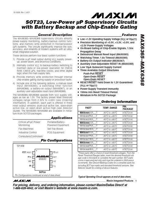
General DescriptionThe MAX6365–MAX6368 supervisory circuits simplify power-supply monitoring, battery-backup control func-tions, and memory write protection in microprocessor (µP) systems. The circuits significantly improve the size,accuracy, and reliability of modern systems with an ultra-small integrated solution.These devices perform four basic system functions:1) Provide a µP reset output during V CC supply power-up, power-down, and brownout conditions.2) Internally control V CC to backup-battery switching tomaintain data or low-power operation for CMOS RAM, CMOS µPs, real-time clocks, and other digital logic when the main supply fails.3) Provide memory write protection through internalchip-enable gating during supply or processor faults.4) Include one of the following options: a manual resetinput (MAX6365), a watchdog timer function (MAX6366), a battery-on output (MAX6367), or an auxiliary user-adjustable reset input (MAX6368).The MAX6365–MAX6368 operate from V CC supply volt-ages as low as 1.2V. The factory preset reset threshold voltages range from 2.32V to 4.63V (see the Ordering Information ). In addition, each part is offered in three reset output versions: push-pull active low, open-drain active low, or open-drain active high (see the Selector Guide ). The MAX6365–MAX6368 are available in minia-ture 8-pin SOT23 packages.ApplicationsCritical µP/µC Power Portable/Battery-Monitoring Powered Equipment Fax Machines Set-Top Boxes Industrial Control POS EquipmentComputers/ControllersFeatures♦Low +1.2V Operating Supply Voltage (V CC or V BATT )♦Precision Monitoring of +5.0V, +3.3V, +3.0V, and +2.5V Power-Supply Voltages♦On-Board Gating of Chip-Enable Signals, 1.5ns Propagation Delay♦Debounced Manual Reset Input (MAX6365)♦Watchdog Timer, 1.6s Timeout (MAX6366)♦Battery-On Output Indicator (MAX6367)♦Auxiliary User-Adjustable RESET IN (MAX6368)♦Low 10µA Quiescent Supply Current ♦Three Available Output StructuresPush-Pull RESET Open-Drain RESET Open-Drain RESET♦RESET/RESET Valid Down to 1.2V Guaranteed (V CC or V BATT )♦Power-Supply Transient Immunity ♦150ms min Reset Timeout Period ♦Miniature 8-Pin SOT23 PackageMAX6365–MAX6368SOT23, Low-Power µP Supervisory Circuits with Battery Backup and Chip-Enable Gating________________________________________________________________Maxim Integrated Products1Pin Configurations19-1658; Rev 3; 12/05For pricing, delivery, and ordering information,please contact Maxim/Dallas Direct!at 1-888-629-4642, or visit Maxim’s website at .Ordering Information*These parts offer a choice of reset threshold voltages. From the Reset Threshold Ranges table, insert the desired threshold volt-age code in the blank to complete the part number. SOT parts come in tape-and-reel only and must be ordered in 2500-piece increments. See Device Marking Codes for a complete parts list,including SOT top marks and standard threshold versions. See Selector Guide for a listing of device features.Devices are available in both leaded and lead-free packaging.Specify lead-free by replacing “-T” with “+T” when ordering.Typical Operating Circuit appears at end of data sheet.M A X 6365–M A X 6368SOT23, Low-Power µP Supervisory Circuits with Battery Backup and Chip-Enable GatingABSOLUTE MAXIMUM RATINGSELECTRICAL CHARACTERISTICS(V = +2.4V to +5.5V, V = +3.0V, CE IN = V , reset not asserted, T = -40°C to +85°C. Typical values are at T = +25°C,Stresses beyond those listed under “Absolute Maximum Ratings” may cause permanent damage to the device. These are stress ratings only, and functional operation of the device at these or any other conditions beyond those indicated in the operational sections of the specifications is not implied. Exposure to absolute maximum rating conditions for extended periods may affect device reliability.Terminal Voltages (with respect to GND)V CC , BATT, OUT.......................................................-0.3V to +6V RESET (open drain), RESET (open drain)................-0.3V to +6V BATT ON, RESET (push-pull), RESET IN,WDI, CE IN, CE OUT...........................-0.3V to (V OUT + 0.3V)MR ..............................................................-0.3V to (V CC + 0.3V)Input CurrentV CC Peak ..............................................................................1A V CC Continuous.............................................................250mA BATT Peak.....................................................................250mA BATT Continuous.............................................................40mAGND...............................................................................75mA Output CurrentOUT...............................Short-Circuit Protected for up to 10s RESET, RESET , BATT ON, CE OUT...............................20mA Continuous Power Dissipation (T A = +70°C)8-Pin SOT23 (derate 8.75mW/°C above +70°C)........700mW Operating Temperature Range ...........................-40°C to +85°C Storage Temperature Range.............................-65°C to +150°C Junction Temperature .....................................................+150°C Lead Temperature (soldering, 10s).................................+300°CMAX6365–MAX6368SOT23, Low-Power µP Supervisory Circuits with Battery Backup and Chip-Enable Gating_______________________________________________________________________________________3ELECTRICAL CHARACTERISTICS (continued)(V CC = +2.4V to +5.5V, V BATT = +3.0V, CE IN = V CC , reset not asserted, T A = -40°C to +85°C. Typical values are at T A = +25°C,M A X 6365–M A X 6368SOT23, Low-Power µP Supervisory Circuits with Battery Backup and Chip-Enable Gating 4_______________________________________________________________________________________Typical Operating Characteristics(T A = +25°C, unless otherwise noted.)8109121115141316-400-2020406080SUPPLY CURRENTvs. TEMPERATURE (NO LOAD)TEMPERATURE (°C)S U P P L Y C U R R E N T (µA )0.20.60.40.81.01.2BATTERY SUPPLY CURRENT (BACKUP MODE) vs. TEMPERATURETEMPERATURE (°C)B A T T E R Y S U P P L YC U R R E N T (µA )-402040-200608021437658-40-2020406080BATT-TO-OUT ON-RESISTANCEvs. TEMPERATURETEMPERATURE (°C)B A T T -T O -O U T O N -R E S I S T A NC E (Ω)ELECTRICAL CHARACTERISTICS (continued)(V= +2.4V to +5.5V, V = +3.0V, CE IN = V , reset not asserted, T = -40°C to +85°C. Typical values are at T = +25°C,Note 2:V BATT can be 0 anytime, or V CC can go down to 0 if V BATT is active (except at startup).Note 3:RESET is pulled up to OUT. Specifications apply for OUT = V CC or OUT = BATT.Note 4:The chip-enable resistance is tested with V CC = V TH(MAX)and CE IN = V CC / 2.MAX6365–MAX6368SOT23, Low-Power µP Supervisory Circuits with Battery Backup and Chip-Enable Gating_______________________________________________________________________________________5Typical Operating Characteristics (continued)(T A = +25°C, unless otherwise noted.)00.40.20.80.61.21.01.4-4020-20406080V CC TO OUT ON-RESISTANCEvs. TEMPERATURETEMPERATURE (°C)V C C T O O U T O N -R E S I S T A N C E (Ω)190195205200210RESET TIMEOUT PERIOD vs. TEMPERATUREM A X 6365/8-05TEMPERATURE (°C)R E S E T T I M E O U T P E R I O D (m s )-402040-206080301575604513512010590TEMPERATURE (°C)P R O P A G A T I O N D E L A Y (µs )-402040-206080V CC TO RESET PROPAGATION DELAYvs. TEMPERATURE2.03.02.55.04.54.03.5RESET THRESHOLD vs. TEMPERATURETEMPERATURE (°C)T H R E S H O L D (V )-402040-206080110010100010,000MAXIMUM TRANSIENT DURATION vs. RESET THRESHOLD OVERDRIVERESET THRESHOLD OVERDRIVE V TH - V CC (mV)M A X I M U M T R A N S I E N T D U R A T I O N (µs )40030035025020005015010003215498761000.5 1.0 1.5 2.0 2.5 3.03.5BATTERY SUPPLY CURRENT vs. SUPPLY VOLTAGEV CC (V)B A T T E R Y S U P P L YC U R R E N T (µA )M A X 6365–M A X 6368SOT23, Low-Power µP Supervisory Circuits with Battery Backup and Chip-Enable Gating 6_______________________________________________________________________________________1.2341.2351.236MAX6368RESET IN THRESHOLD vs. TEMPERATUREM A X 6365/8 -10TEMPERATURE (°C)V R T H (V )-402040-2060801.01.91.61.32.82.52.2MAX6368RESET IN TO RESET PROPAGATION DELAYvs. TEMPERATURETEMPERATURE (°C)P R O P A G A T I O N D E L A Y (µs )-402040-206080013245C LOAD (pF)P R O P A G A T I O N D E L A Y (n s )10050150200CHIP-ENABLE PROPAGATION DELAY vs. CE OUT LOAD CAPACITANCE515102025-40-2020406080TEMPERATURE (°C)C E I N T O C E O U T O N -R E S I S T A N C E (Ω)CE IN TO CE OUT ON-RESISTANCEvs. TEMPERATURE1.01.31.21.11.51.41.91.81.71.62.0-40-2020406080TEMPERATURE (°C)W A T C H D O G T I M E O U T P E R I O D (s )MAX6366WATCHDOG TIMEOUT PERIODvs. TEMPERATURETypical Operating Characteristics (continued)(T A = +25°C, unless otherwise noted.)MAX6365–MAX6368SOT23, Low-Power µP Supervisory Circuits with Battery Backup and Chip-Enable Gating_______________________________________________________________________________________7M A X 6365–M A X 6368SOT23, Low-Power µP Supervisory Circuits with Battery Backup and Chip-Enable Gating 8_______________________________________________________________________________________Detailed DescriptionThe Typical Operating Circuit shows a typical connec-tion for the MAX6365–MAX6368. OUT powers the static random-access memory (SRAM). If V CC is greater than the reset threshold (V TH ), or if V CC is lower than V TH but higher than V BATT , V CC is connected to OUT. If V CC is lower than V TH and V CC is less than V BATT ,BATT is connected to OUT. OUT supplies up to 150mA from V CC . In battery-backup mode, an internal MOSFET connects the backup battery to OUT. The on-resistance of the MOSFET is a function of backup-battery voltage and is shown in the BATT-to-OUT On-Resistance vs.Temperature graph in the T ypical Operating Char-acteristics .Chip-Enable Signal GatingThe MAX6365–MAX6368 provide internal gating of CE signals to prevent erroneous data from being written toCMOS RAM in the event of a power failure. During nor-mal operation, the CE gate is enabled and passes all CE transitions. When reset asserts, this path becomes disabled, preventing erroneous data from corrupting the CMOS RAM. All of these devices use a series trans-mission gate from CE IN to CE OUT. The 2ns propaga-tion delay from CE IN to CE OUT allows the devices to be used with most µPs and high-speed DSPs.During normal operation, CE IN is connected to CE OUT through a low on-resistance transmission gate.This is valid when reset is not asserted. If CE IN is high when reset is asserted, CE OUT remains high regard-less of any subsequent transitions on CE IN during the reset event.If CE IN is low when reset is asserted, CE OUT is held low for 12µs to allow completion of the read/write oper-ation (F igure 1). After the 12µs delay expires, the CEFunctional DiagramMAX6365–MAX6368SOT23, Low-Power µP Supervisory Circuits with Battery Backup and Chip-Enable Gating_______________________________________________________________________________________9OUT goes high and stays high regardless of any sub-sequent transitions on CE IN during the reset event.When CE OUT is disconnected from CE IN, CE OUT is actively pulled up to OUT.The propagation delay through the chip-enable circuit-ry depends on both the source impedance of the drive to CE IN and the capacitive loading at CE OUT. The chip-enable propagation delay is production tested from the 50% point of CE IN to the 50% point of CE OUT, using a 50Ωdriver and 50pF load capacitance.Minimize the capacitive load at CE OUT to minimize propagation delay, and use a low-output-impedance driver.Backup-Battery SwitchoverIn a brownout or power failure, it may be necessary to preserve the contents of the RAM. With a backup bat-tery installed at BATT, the MAX6365–MAX6368 auto-matically switch the RAM to backup power when V CC falls. The MAX6367 has a BATT ON output that goes high in battery-backup mode. These devices require two conditions before switching to battery-backup mode:1) V CC must be below the reset threshold.2) V CC must be below V BATT .Table 1 lists the status of the inputs and outputs in bat-tery-backup mode. The devices do not power up if the only voltage source is on BATT. OUT only powers upfrom V CC at startup.Many µP-based products require manual reset capabili-ty, allowing the user or external logic circuitry to initiate a reset. For the MAX6365, a logic low on MR asserts reset.Reset remains asserted while MR is low and for a mini-mum of 150ms (t RP ) after it returns high. MR has an inter-nal 20k Ωpullup resistor to V CC . This input can be driven with TTL/CMOS logic levels or with open-drain/collector outputs. Connect a normally open momentary switch from MR to GND to create a manual reset function; exter-nal debounce circuitry is not required. If MR is driven from long cables or the device is used in a noisy environ-ment, connect a 0.1µF capacitor from MR to GND to pro-vide additional noise immunity.Figure 1. Reset and Chip-Enable TimingM A X 6365–M A X 6368SOT23, Low-Power µP Supervisory Circuits with Battery Backup and Chip-Enable Gating 10______________________________________________________________________________________Watchdog Input (MAX6366 Only)The watchdog monitors µP activity through the watch-dog input (WDI). If the µP becomes inactive, reset asserts. To use the watchdog function, connect WDI to a bus line or µP I/O line. A change of state (high to low,low to high, or a minimum 100ns pulse) resets the watchdog timer. If WDI remains high or low for longer than the watchdog timeout period (t WD ), the internal watchdog timer runs out and a reset pulse is triggered for the reset timeout period (t RP ). The internal watchdog timer clears whenever reset asserts or whenever WDI sees a rising or falling edge. If WDI remains in either a high or low state, a reset pulse asserts periodically after every t WD (Figure 2).BATT ON Indicator (MAX6367 Only)BATT ON is a push-pull output that drives high when in battery-backup mode. BATT ON typically sinks 3.2mA at 0.1V saturation voltage. In battery-backup mode, this terminal sources approximately 10µA from OUT. Use BATT ON to indicate battery-switchover status or to supply base drive to an external pass transistor for higher current applications (Figure 3).RESET IN Comparator (MAX6368 Only)RESET IN is compared to an internal 1.235V reference.If the voltage at RESET IN is less than 1.235V, reset asserts. Use the RESET IN comparator as an undervolt-age detector to signal a failing power supply or as a secondary power-supply reset monitor.To program the reset threshold (V RTH ) of the secondary power supply, use the following (see Typical Operating Circuit ):V RTH = V REF (R1 / R2 + 1)where V REF = 1.235V. To simplify the resistor selection,choose a value for R2 and calculate R1:R1 = R2 [(V RTH / V REF ) - 1]Since the input current at RESET IN is 25nA (max),large values (up to 1M Ω) can be used for R2 with no significant loss in accuracy. For example, in the Typical Operating Circuit , the MAX6368 monitors two supply voltages. To monitor the secondary 5V logic or analog supply with a 4.60V nominal programmed reset thresh-old, choose R2 = 100k Ω, and calculate R1 = 273k Ω.Reset OutputA µP’s reset input starts the µP in a known state. The MAX6365–MAX6368 µP supervisory circuits assert a reset to prevent code-execution errors during power-up, power-down, and brownout conditions. RESET is guaranteed to be a logic low or logic high, depending on the device chosen (see the Ordering Information ).RESET or RESET asserts when V CC is below the reset threshold and for at least 150ms (t RP ) after V CC rises above the reset threshold. RESET or RESET also asserts when MR is low (MAX6365) and when RESET IN is less than 1.235V (MAX6368). The MAX6366 watch-dog function will cause RESET (or RESET ) to assert in pulses following a watchdog timeout (Figure 2).Applications InformationOperation Withouta Backup Power SourceThe MAX6365–MAX6368 provide battery-backup func-tions. If a backup power source is not used, connect BATT to GND and OUT to V CC .Watchdog Software ConsiderationsOne way to help the watchdog timer monitor the soft-ware execution more closely is to set and reset the watchdog at different points in the program rather than pulsing the watchdog input periodically. F igure 4shows a flow diagram in which the I/O driving theFigure 2. MAX6366 Watchdog Timeout Period and Reset Active TimeMAX6365–MAX6368SOT23, Low-Power µP Supervisory Circuits with Battery Backup and Chip-Enable Gating______________________________________________________________________________________11watchdog is set low in the beginning of the program,set high at the beginning of every subroutine or loop,and set low again when the program returns to the beginning. If the program should hang in any subrou-tine, the problem would be quickly corrected.Replacing the Backup BatteryWhen V CC is above V TH , the backup power source can be removed without danger of triggering a reset pulse.The device does not enter battery-backup mode when V CC stays above the reset threshold voltage.Negative-Going V CC TransientsThese supervisors are relatively immune to short-dura-tion, negative-going V CC transients. Resetting the µP when V CC experiences only small glitches is usually not desirable.The T ypical Operating Characteristics section has a Maximum Transient Duration vs. Reset Threshold Overdrive graph for which reset is not asserted. The graph was produced using negative-going V CC pulses,starting at V CC and ending below the reset threshold by the magnitude indicated (reset threshold overdrive).The graph shows the maximum pulse width that a neg-ative-going V CC transient can typically have without triggering a reset pulse. As the amplitude of the tran-sient increases (i.e., goes further below the reset threshold), the maximum allowable pulse width decreases. Typically, a V CC transient that goes 100mV below the reset threshold and lasts for 30µs will not trig-ger a reset pulse.A 0.1µF bypass capacitor mounted close to the V CC pin provides additional transient immunity.M A X 6365–M A X 6368SOT23, Low-Power µP Supervisory Circuits with Battery Backup and Chip-Enable Gating 12______________________________________________________________________________________standard versions only. Contact factory for availability of nonstandard versions.MAX6365–MAX6368SOT23, Low-Power µP Supervisory Circuits with Battery Backup and Chip-Enable Gating______________________________________________________________________________________13Pin Configurations (continued)M A X 6365–M A X 6368SOT23, Low-Power µP Supervisory Circuits with Battery Backup and Chip-Enable Gating 14______________________________________________________________________________________Typical Operating CircuitChip InformationTRANSISTOR COUNT: 729PROCESS: CMOSSOT23, Low-Power µP Supervisory Circuits with Battery Backup and Chip-Enable GatingMAX6365–MAX6368Maxim cannot assume responsibility for use of any circuitry other than circuitry entirely embodied in a Maxim product. No circuit patent licenses are implied. Maxim reserves the right to change the circuitry and specifications without notice at any time.Maxim Integrated Products, 120 San Gabriel Drive, Sunnyvale, CA 94086 408-737-7600 ____________________15©2005 Maxim Integrated ProductsPrinted USAis a registered trademark of Maxim Integrated Products, Inc.Package Information(The package drawing(s) in this data sheet may not reflect the most current specifications. For the latest package outline information go to /packages .)。