OB2358俊
- 格式:pdf
- 大小:180.24 KB
- 文档页数:1


TI型号⼤全35-迈锐国际ADC0820CCWMX/NOPB SOIC-201000EAR99TI迈锐国际胡浩亮137********ADC082S021CIMM/NOPB VSSOP-81000EAR99TI迈锐国际胡浩亮137********ADC082S021CIMMX/NOPB VSSOP-83500EAR99TI迈锐国际胡浩亮137********ADC082S051CIMM/NOPB VSSOP-81000EAR99TI迈锐国际胡浩亮137********ADC082S101CIMM/NOPB VSSOP-81000EAR99TI迈锐国际胡浩亮137********ADC082S101CIMMX/NOPB VSSOP-83500EAR99TI迈锐国际胡浩亮137********ADC083000CIYB/NOPB HLQFP-1286003A001A5A1TI迈锐国际胡浩亮137********ADC083000CIYB/S7002214HLQFP-1286003A001A5A1TI迈锐国际胡浩亮137********ADC0831CCN/NOPB PDIP-81000EAR99TI迈锐国际胡浩亮137********ADC0831CCWM/NOPB SOIC-143000EAR99TI迈锐国际胡浩亮137********ADC0831CCWMX/NOPB SOIC-141000EAR99TI迈锐国际胡浩亮137********ADC0832CCN/NOPB PDIP-81000EAR99TI迈锐国际胡浩亮137********ADC0832CCWM/NOPB SOIC-143000EAR99TI迈锐国际胡浩亮137********ADC0832CCWMX/NOPB SOIC-141000EAR99TI迈锐国际胡浩亮137********ADC0834CCN/NOPB PDIP-14500EAR99TI迈锐国际胡浩亮137********ADC0834CCWM/NOPB SOIC-143000EAR99TI迈锐国际胡浩亮137********ADC0834CCWMX/NOPB SOIC-141000EAR99TI迈锐国际胡浩亮137********ADC08351CILQE/NOPB WQFN-24250EAR99TI迈锐国际胡浩亮137********ADC08351CILQX/NOPB WQFN-244500EAR99TI迈锐国际胡浩亮137********ADC08351CIMTCE/NOPB TSSOP-20250EAR99TI迈锐国际胡浩亮137********ADC08351CIMTCX/NOPB TSSOP-202500EAR99TI迈锐国际胡浩亮137********ADC08351EVM RFIDSUB01EAR99TI迈锐国际胡浩亮137********ADC0838CCWM/NOPB SOIC-202160EAR99TI迈锐国际胡浩亮137********ADC0838CCWMX/NOPB SOIC-201000EAR99TI迈锐国际胡浩亮137********ADC0838CIWM/NOPB SOIC-202160EAR99TI迈锐国际胡浩亮137********ADC0838CIWMX/NOPB SOIC-201000EAR99TI迈锐国际胡浩亮137********ADC0848BCV/NOPB PLCC-281750EAR99TI迈锐国际胡浩亮137********ADC0848BCVX/NOPB PLCC-28750EAR99TI迈锐国际胡浩亮137********ADC0848CCV/NOPB PLCC-281750EAR99TI迈锐国际胡浩亮137******** ADC0848CCVX/NOPB PLCC-28750EAR99TI迈锐国际胡浩亮137********ADC084S021CIMM/J7001218VSSOP-101000EAR99TI迈锐国际胡浩亮137********ADC084S021CIMM/NOPB VSSOP-101000EAR99TI迈锐国际胡浩亮137********ADC084S021CIMMX/NOPB VSSOP-103500EAR99TI迈锐国际胡浩亮137********ADC084S051CIMM/NOPB VSSOP-101000EAR99TI迈锐国际胡浩亮137********ADC084S101CIMM/NOPB VSSOP-101000EAR99TI迈锐国际胡浩亮137********ADC08500CIYB/NOPB HLQFP-1286003A991C1TI迈锐国际胡浩亮137********ADC08831IM SOIC-89500EAR99TI迈锐国际胡浩亮137********ADC08831IM/NOPB SOIC-89500EAR99TI迈锐国际胡浩亮137********ADC08831IMX/NOPB SOIC-82500EAR99TI迈锐国际胡浩亮137********ADC08832IMM/NOPB VSSOP-81000EAR99TI迈锐国际胡浩亮137********ADC08832IM/NOPB SOIC-89500EAR99TI迈锐国际胡浩亮137********ADC08832IMX/NOPB SOIC-82500EAR99TI迈锐国际胡浩亮137********ADC088S022CIMT TSSOP-169200EAR99TI迈锐国际胡浩亮137********ADC088S022CIMT/NOPB TSSOP-169200EAR99TI迈锐国际胡浩亮137********ADC088S022CIMTX/NOPB TSSOP-162500EAR99TI迈锐国际胡浩亮137********ADC088S052CIMT/NOPB TSSOP-169200EAR99TI迈锐国际胡浩亮137********ADC088S052CIMTX/NOPB TSSOP-162500EAR99TI迈锐国际胡浩亮137********ADC088S102CIMT/NOPB TSSOP-169200EAR99TI迈锐国际胡浩亮137********ADC088S102CIMTX/NOPB TSSOP-162500EAR99TI迈锐国际胡浩亮137********ADC08B200CIVS/NOPB TQFP-482500EAR99TI迈锐国际胡浩亮137********ADC08B200QCIVS/NOPB TQFP-482500EAR99TI迈锐国际胡浩亮137********ADC08B3000CIYB/NOPB HLQFP-1286003A991C1TI迈锐国际胡浩亮137********ADC08B3000RB/NOPB RFIDSUB01EAR99TI迈锐国际胡浩亮137********ADC08D1000CIYB/NOPB HLQFP-1286003A001A5A1TI迈锐国际胡浩亮137********ADC08D1010DIYB/NOPB HLQFP-1286003A001A5A1TI迈锐国际胡浩亮137********ADC08D1020CIYB/NOPB HLQFP-1286003A001A5A1TI迈锐国际胡浩亮137********ADC08D1500CIYB/NOPB HLQFP-1286003A001A5A1TI迈锐国际胡浩亮137********ADC08D1520CIYB/NOPB HLQFP-1286003A001A5A1TI迈锐国际胡浩亮137********ADC08D1520CIYB/S7002396HLQFP-1286003A001A5A1TI迈锐国际胡浩亮137********ADC08D1520CVAL RFIDSUB013A002H1A TI迈锐国际胡浩亮137********迈锐国际胡浩亮ADC08D1520RB/NOPB RFIDSUB013A002H1A TI137******** ADC08D1520WGFQV CQFP-128243A001A2C TI迈锐国际胡浩亮137********ADC08D1520WGMPR CQFP-128243A001A5A1TI迈锐国际胡浩亮137********ADC08D500CIYB/NOPB HLQFP-1286003A991C1TI迈锐国际胡浩亮137********ADC08D500CIYB/S7002554HLQFP-1286003A991C1TI迈锐国际胡浩亮137********ADC08D500CIYB/S7002952HLQFP-1286003A991C1TI迈锐国际胡浩亮137********ADC08D502CIYB/NOPB HLQFP-1286003A991C1TI迈锐国际胡浩亮137********ADC08DJ3200AAV FCBGA-1448403A001A5A1TI迈锐国际胡浩亮137********ADC08DJ3200AAVT FCBGA-1442503A001A5A1TI迈锐国际胡浩亮137********ADC08DJ3200EVM UNKNOWN-14413A002H1A TI迈锐国际胡浩亮137********ADC08DL500CIVV/NOPB LQFP-1446003A991C1TI迈锐国际胡浩亮137********ADC08DL502CIVV/NOPB LQFP-1446003A991C1TI迈锐国际胡浩亮137********ADC08L060CIMT/NOPB TSSOP-246100EAR99TI迈锐国际胡浩亮137********ADC08L060CIMTX/NOPB TSSOP-242500EAR99TI迈锐国际胡浩亮137********ADC08L060EVM RFIDSUB01EAR99TI迈锐国际胡浩亮137********ADC09QJ1300EVM RFIDSUB01EAR99TI迈锐国际胡浩亮137********ADC10040CIMT/NOPB TSSOP-284800EAR99TI迈锐国际胡浩亮137********ADC10040CIMTX/NOPB TSSOP-282500EAR99TI迈锐国际胡浩亮137********ADC10040QCIMT/NOPB TSSOP-284800EAR99TI迈锐国际胡浩亮137********ADC10040QCIMTX/NOPB TSSOP-282500EAR99TI迈锐国际胡浩亮137********ADC10065CIMT/NOPB TSSOP-284800EAR99TI迈锐国际胡浩亮137********ADC10065CIMTX/NOPB TSSOP-282500EAR99TI迈锐国际胡浩亮137********ADC10080CIMT/NOPB TSSOP-284800EAR99TI迈锐国际胡浩亮137********ADC10080CIMTX/NOPB TSSOP-282500EAR99TI迈锐国际胡浩亮137********ADC101C021CIMK/NOPB SOT-23-THN-61000EAR99TI迈锐国际胡浩亮137********ADC101C021CIMKX/NOPB SOT-23-THN-63000EAR99TI迈锐国际胡浩亮137********ADC101C021CIMM/NOPB VSSOP-81000EAR99TI迈锐国际胡浩亮137********ADC101C027CIMK/NOPB SOT-23-THN-61000EAR99TI迈锐国际胡浩亮137********ADC101C027CIMKX/NOPB SOT-23-THN-63000EAR99TI迈锐国际胡浩亮137********ADC101S021CIMF/NOPB SOT-23-61000EAR99TI迈锐国际胡浩亮137********ADC101S021CIMFX/NOPB SOT-23-63000EAR99TI迈锐国际胡浩亮137********迈锐国际胡浩亮ADC101S021CISD/NOPB WSON-61000EAR99TI137********ADC101S021CISDX/NOPB WSON-64500EAR99TI迈锐国际胡浩亮137********ADC101S051CIMF/NOPB SOT-23-61000EAR99TI迈锐国际胡浩亮137********ADC101S051CIMFX/NOPB SOT-23-63000EAR99TI迈锐国际胡浩亮137********ADC101S051QIMF/NOPB SOT-23-61000EAR99TI迈锐国际胡浩亮137********ADC101S051QIMFX/NOPB SOT-23-63000EAR99TI迈锐国际胡浩亮137********ADC101S101CIMF/NOPB SOT-23-61000EAR99TI迈锐国际胡浩亮137********ADC101S101CIMFX/NOPB SOT-23-63000EAR99TI迈锐国际胡浩亮137********ADC101S101CISD/NOPB WSON-61000EAR99TI迈锐国际胡浩亮137********。

NMB24-3FootnotesBasic Non Fail-Safe actuator for controlling dampers in typical commercial HVAC applications.• Torque motor 90 in-lb [10 Nm]• Nominal voltage AC/DC 24 V • Control On/Off, Floating pointTechnical dataElectrical dataNominal voltageAC/DC 24 V Nominal voltage frequency 50/60 HzNominal voltage rangeAC 19.2...28.8 V / DC 21.6...28.8 V Power consumption in operation 2 W Power consumption in rest position 0.2 W Transformer sizing 4 VAOverload Protectionelectronic throughout 0...95° rotation Functional dataTorque motor90 in-lb [10 Nm]Direction of motion motor selectable with switch 0/1Manual override external push button Angle of rotation Max. 95°Angle of rotation note adjustable with mechanical stop Running Time (Motor)95 s / 90°Running time motor note constant, independent of load Noise level, motor 45 dB(A)Position indicationMechanical, 30...65 mm stroke Safety dataPower source ULClass 2 Supply Degree of protection IEC/EN IP54Degree of protection NEMA/UL NEMA 2Enclosure UL Enclosure Type 2Agency ListingcULus acc. to UL60730-1A/-2-14, CAN/CSA E60730-1:02CE acc. to 2014/30/EU and 2014/35/EU Quality Standard ISO 9001UL 2043 CompliantSuitable for use in air plenums per Section 300.22(C) of the NEC and Section 602 of the IMCAmbient humidity Max. 95% RH, non-condensing Ambient temperature -22...122°F [-30...50°C]Storage temperature -40...176°F [-40...80°C]Servicingmaintenance-free Weight Weight2.9 lb [0.94 kg]MaterialsHousing material UL94-5VA†Rated Impulse Voltage 800V, Type action 1, Control Pollution Degree 3.NMB24-3ApplicationOperationTypical specificationProduct featuresFor on/off and floating point control of dampers in HVAC systems. Actuator sizing should be done in accordance with the damper manufacturer’s specifications.The actuator is mounted directly to a damper shaft up to 1.05” in diameter by means of its universal clamp. A crank arm and several mounting brackets are available for applications where the actuator cannot be direct coupled to the damper shaft.The actuator is not provided with and does not require any limit switches, but is electronically protected against overload. The anti-rotation strap supplied with the actuator will prevent lateral movement.The NMB(X) series provides 95° of rotation and a visual indicator indicates position of theactuator. When reaching the damper or actuator end position, the actuator automatically stops. The gears can be manually disengaged with a button on the actuator cover.The NMB(X)24-3… actuators use a sensorless brushless DC motor, which is controlled by an Application Specific Integrated Circuit (ASIC). The ASIC monitors and controls the actuator’s rotation and provides a digital rotation sensing (DRS) function to prevent damage to the actuator in a stall condition. Power consumption is reduced in holding mode.Add-on auxiliary switches or feedback potentiometers are easily fastened directly onto the actuator body for signaling and switching functions.Floating point, on/off control damper actuators shall be electronic direct-coupled type, which require no crank arm and linkage and be capable of direct mounting to a shaft up to 1.05”diameter. Actuators shall have brushless DC motor technology and be protected from overload at all angles of rotation. Actuators shall have reversing switch and manual override on the cover. If required, actuators will be provided with a screw terminal strip for electricalconnections (NMX24-3-T). Run time shall be constant and independent of torque. Actuators shall be cULus listed, have a 5-year warranty, and be manufactured under ISO 9001 International Quality Control Standards. Actuators shall be as manufactured by Belimo.AccessoriesElectrical accessoriesDescriptionType Battery backup system, for non-spring return models NSV24 US Battery, 12 V, 1.2 Ah (two required)NSV-BAT Auxiliary switch 1 x SPDT add-on S1A Auxiliary switch 2 x SPDT add-onS2AFeedback potentiometer 140 Ω add-on, grey P140A GR Feedback potentiometer 1 kΩ add-on, grey P1000A GR Feedback potentiometer 10 kΩ add-on, grey P10000A GR Feedback potentiometer 2.8 kΩ add-on, grey P2800A GR Feedback potentiometer 500 Ω add-on, grey P500A GR Feedback potentiometer 5 kΩ add-on, greyP5000A GR Mechanical accessoriesDescriptionType Shaft clamp reversible, clamping range ø8...20 mm K-NA Mounting bracket for AF..ZG-100Mounting bracket ZG-101Mounting bracket ZG-103Mounting bracketZG-104Mounting kit for linkage operation for flat installationZG-NMA Shaft extension 240 mm ø20 mm for damper shaft ø8...22.7 mm AV8-25Shaft extension for 1/2" diameter shafts (3.8" L).ZG-NMSA-1Weather shield 13x8x6" [330x203x152 mm] (LxWxH)ZS-100Weather shield 406x213x102 mm [16x8-3/8x4"] (LxWxH)ZS-150Wrench 0.32 in and 0.39 in [8 mm and 10 mm]TOOL-06Linkage kitJackshaft Retrofit Linkage with Belimo Rotary ActuatorsZG-JSLElectrical installationActuators with appliance cables are numbered.Provide overload protection and disconnect as required.NMB24-3Actuators may also be powered by DC 24 V.Actuators Hot wire must be connected to the control board common. Only connect common toneg. (-) leg of control circuits. Terminal models (-T) have no-feedback.Actuators may be connected in parallel if not mechanically linked. Power consumption andinput impedance must be observed.Floating Point - Triac SourceWiring diagramsOn/Off Floating PointFloating Point - Triac Source Floating Point - Triac SinkNMB24-3 Dimensions。

SymbolTyp Max 14.2203950R θJC 0.8 1.5Maximum Junction-to-AmbientASteady-State °C/W Maximum Junction-to-CaseCSteady-State°C/WThermal Characteristics ParameterUnits Maximum Junction-to-Ambient At ≤ 10s R θJA °C/W AOD438AOD438SymbolMin TypMaxUnits BV DSS 30V 1T J =55°C5I GSS 100nA V GS(th)1 1.83V I D(ON)85A 2.8 3.5T J =125°C4.45.54.4 5.5m Ωg FS 106S V SD 0.721V I S85A C iss 32003840pF C oss 590pF C rss 414pF R g0.540.7ΩQ g (10V)6376nC Q g (4.5V)3340nC Q gs 8.6nC Q gd 17.6nC t D(on)12ns t r 15.5ns t D(off)40ns t f 14ns t rr 3441ns Q rr30nCTHIS PRODUCT HAS BEEN DESIGNED AND QUALIFIED FOR THE CONSUMER MARKET. APPLICATIONS OR USES AS CRITICAL COMPONENTS IN LIFE SUPPORT DEVICES OR SYSTEMS ARE NOT AUTHORIZED. AOS DOES NOT ASSUME ANY LIABILITY ARISING OUT OF SUCH APPLICATIONS OR USES OF ITS PRODUCTS. AOS RESERVES THE RIGHT TO IMPROVE PRODUCT DESIGN,FUNCTIONS AND RELIABILITY WITHOUT NOTICE.Gate Drain Charge V GS =0V, V DS =15V, f=1MHz SWITCHING PARAMETERS Total Gate Charge Gate Source Charge Gate resistanceV GS =0V, V DS =0V, f=1MHzV GS =4.5V, V DS =15V, I D =20ATotal Gate Charge Turn-On Rise Time Turn-Off DelayTime V GS =10V, V DS =15V, R L =0.75Ω, R GEN =3ΩTurn-Off Fall TimeTurn-On DelayTime m ΩV GS =4.5V, I D =20AI S =1A,V GS =0VV DS =5V, I D =20AMaximum Body-Diode Continuous CurrentInput Capacitance Output CapacitanceDYNAMIC PARAMETERS R DS(ON)Static Drain-Source On-ResistanceForward TransconductanceDiode Forward Voltage I DSS µA Gate Threshold Voltage V DS =V GS I D =250µA V DS =24V, V GS =0VV DS =0V, V GS = ±20V Zero Gate Voltage Drain Current Gate-Body leakage current Electrical Characteristics (T J =25°C unless otherwise noted)STATIC PARAMETERS Parameter Conditions Body Diode Reverse Recovery TimeBody Diode Reverse Recovery Charge I F =20A, dI/dt=100A/µsDrain-Source Breakdown Voltage On state drain currentI D =250µA, V GS =0V V GS =10V, V DS =5V V GS =10V, I D =20AReverse Transfer Capacitance I F =20A, dI/dt=100A/µsA: The value of R θJA is measured with the device mounted on 1in 2 FR-4 board with 2oz. Copper, in a still air environment with T A =25°C. The Power dissipation P DSM is based on steady-state R θJA and the maximum allowed junction temperature of 150°C. The value in any givenapplication depends on the user's specific board design, and the maximum temperature of 175°C may be used if the PCB or heatsink allows it.B. The power dissipation P D is based on T J(MAX)=175°C, using junction-to-case thermal resistance, and is more useful in setting the upperdissipation limit for cases where additional heatsinking is used. It is used to determine the current rating, when this rating falls below the package limit.C: Repetitive rating, pulse width limited by junction temperature T J(MAX)=175°C.D. The R θJA is the sum of the thermal impedence from junction to case R θJC and case to ambient.E. The static characteristics in Figures 1 to 6 are obtained using <300 µs pulses, duty cycle 0.5% max.F. These tests are performed with the device mounted on 1 in 2 FR-4 board with 2oz. Copper, in a still air environment with T A =25°C. The SOA curve provides a single pulse rating.G. The maximum current rating is limited by the package current capability. Rev 2: July 2005AOD438AOD438AOD438。

astm f2358 蓝宝石衬底的特征测量标准指南ASTM F2358 蓝宝石衬底的特征测量标准指南ASTM F2358是美国材料和试验协会(ASTM)发布的一项技术标准,旨在为蓝宝石衬底的特征测量提供指导。
蓝宝石衬底在多个领域中都具有重要的应用,如电子、光学和医疗器械等,因此其质量和特征测量的标准化显得尤为重要。
本文将从多个角度深入探讨ASTM F2358标准,希望能够为您全面理解和应用这一标准提供帮助。
1. 背景介绍ASTM F2358标准是针对蓝宝石衬底的特征测量而制定的。
蓝宝石衬底是一种用于支撑和保护其他材料的基板材料,其特征测量对于确保其他材料的性能和稳定性具有重要意义。
ASTM F2358标准的制定旨在规范蓝宝石衬底的特征测量方法,以确保其质量和可靠性。
2. 标准内容概述ASTM F2358标准主要包括蓝宝石衬底特征测量的一般原则、测量方法和设备要求等内容。
其中,关于测量方法的规定包括了蓝宝石衬底表面形貌、尺寸、厚度、结构等多个方面的具体测量方法,以及相应的测量设备要求。
该标准的发布,为蓝宝石衬底的特征测量提供了统一的标准和方法,有利于提高其质量和可信度。
3. 标准应用领域ASTM F2358标准适用于多个领域,包括但不限于电子、光学、医疗器械等领域。
在电子领域,蓝宝石衬底常用于制备集成电路等器件,其表面形貌、尺寸和厚度等特征直接影响器件的性能和稳定性。
在光学领域,蓝宝石衬底可用于制备激光器、光学镜片等产品,其质量和特征测量对于保证产品的光学性能至关重要。
在医疗器械领域,蓝宝石衬底常用于制备手术刀片等产品,其表面形貌和结构特征直接关系到产品的使用效果和安全性。
ASTM F2358标准的适用范围广泛,对于确保相关产品的质量和性能具有重要意义。
4. 个人观点和理解从本标准的制定背景和内容来看,我个人认为ASTM F2358标准的发布对于推动蓝宝石衬底行业的规范化和标准化具有重要意义。
作为一种重要的基板材料,蓝宝石衬底在多个领域中都具有广泛的应用前景,其质量和特征测量的标准化将有助于提高产品质量和可靠性,推动相关行业的发展和进步。


OB2353 设计指导-反激式开关电源应用一.概要:电子技术的不断的发展,各式各样的电子产品遍及世界每一个角落,开关电源的市场随着电子设备的不断发展也越来越大,同时市场对电源的要求也不断提高。
节能,高效,小体积,低成本,高性价比成了电源发展的主流趋势。
昂宝电子在这样的市场背景下,适时的向市场推出一款PWM控制芯片OB2353,让系统能很轻易的达到以上的要求。
OB2353具有如下特性:▲内置开关管:OB2353内含开关管,简化了系统电路设计,减少了系统的元器件个数,增加了系统的可靠性,为客户在市场竞争中取得优势。
▲软启动:OB2353提供了4mS的软启动时间。
在这段时间内,芯片的最大占空比由小到大逐渐得到释放,大大降低了系统的过冲及元器件应力。
同时也提高了系统的可靠性。
▲低待机功耗:OB2353通过特别的低功耗间歇工作模式设计不仅可以让整个系统在空载的状态下轻易达到国际能源机构最新的推荐标准,而且允许系统在较轻负载的情况下同样具有超低耗,高能源转换率的性能。
▲固定工作频率:OB2353具有固定的工作频率,中心频率在50KHZ左右,这样为系统节省了一颗频率电阻,使PCB布板更简单,而且还可以避免由于布板不佳而引起的干扰,提高系统的稳定性。
▲无噪声工作:使用OB2353设计的电源无论在空载,轻载和满载的情况下都不会产生音频噪声。
优化的系统设计可以使系统在任何工作状态下均可安静地工作。
▲内置斜率补偿:芯片内含斜率补偿功能,使系统在不同的占空比下保持稳定工作。
▲更低启动电流:OB2353启动电流低至5uA,可有效地减少系统启动电路的损耗,缩短系统的启动时间。
▲更低工作电流:OB2353的工作电流约为1.6mA,可有效降低系统的损耗,提高系统的效率。
▲内置前沿消隐:内置前沿消隐(LEB),可以为系统节省一个外部的R-C网络,降低系统成本,增加系统的稳定性。
▲内置AC高低压OCP补偿:OB2353内置了OCP补偿功能,使系统在不需要增加成本的情况下轻易使得全电压范围内系统的OCP曲线趋向平坦,提高系统的性价比。

DESCRIPTION Isolated μModule DC/DC Converterwith LDO RegulatorThe Demo Circuit 2358A is a 2kV AC isolated flyback μModule® DC/DC converter with LDO post regulator featur-ing the LTM8068. The demo circuit is designed for a 5.6V flyback output and a 5V post regulator output from a 4.5V to 40V input. The current capability of the 5.6V flyback output varies with input voltage from about 200mA at 4.5V IN to about 460mA at 40V IN. The current capability of the 5V LDO output is limited by either the current capabil-ity of V OUT1 minus V OUT1 loading or the 300mA current limit on the LDO post regulator itself. Figure 1 shows the maximum output current on V OUT1 when V OUT2 is notloaded, and V OUT2 when V OUT1 is unloaded. V OUT2 is the LDO post regulator from V OUT1.L, L T, L TC, L TM, Linear Technology, the Linear logo and µModule are registered trademarks of Linear Technology Corporation. All other trademarks are the property of their respective owners. The two-stage converter provides an isolated flyback output as well as a low-noise LDO output. Figure 2 shows the output noise spectrum on the flyback output and Figure 3 shows the output noise spectrum on the LDO output. The LTM8068 data sheet gives complete description of the device, operation and application information. The data sheet must be read in conjunction with this quick start guide for demo circuit 2358A.Design files for this circuit board are available at /demo/DC2358ABOARD PHOTO1dc2358af2dc2358afPERFORMANCE SUMMARYPARAMETER CONDITIONSMINTYPMAX UNITSMinimum Input Voltage 4.5V Maximum Input Voltage 40V Output Voltage V OUT1 V IN = 4.5V to 40V 5.3 5.6 5.9V Output Voltage V OUT2V IN = 4.5V to 40V4.855 5.15V Voltage Ripple V OUT1V IN = 12V, I OUT1 = 200mA, I OUT2 = 0mA 25mV Voltage Ripple V OUT2V IN = 12V, I OUT1 = 0mA, I OUT2 = 200mA1mVDemo circuit 2358A is easy to set up to evaluate the per-formance of the LTM8068. Refer to Figure 4 for proper measurement equipment setup and follow the procedure below:NOTE: When measuring the input or output voltage ripple, care must be taken to avoid a long ground lead on the oscilloscope probe. Measure the input or output voltage ripple by touching the probe tip directly across the V IN and GND or V OUT and V OUTN terminals. See Figure 5 for proper scope probe technique.1. With power off, connect the input power supply to V IN and GND.2. Turn on the power at the input.NOTE. Make sure that the input voltage does notexceed 40V.3. Check for the proper output voltages. (For OUT1, check the voltage between V OUT1 and V OUTN . For OUT2, check the voltage between V OUT2 and V OUTN .) NOTE: If there is no output, temporarily disconnect the load to make sure that the load is not set too high.4. Once the proper output voltages are established, adjust the load within the operating range and observe the output voltage regulation, ripple voltage, efficiency and other parameters.QUICK START PROCEDURESpecifications are at T A = 25°CFigure 1. Maximum Output Current vs V IN : 5.6V OUT1 Flyback Output with V OUT2 Unloaded; 5V OUT2 LDO output with V OUT1 UnloadedFigure 2. V OUT1 Output Noise Spectrum with I OUT1 at 200mA and V IN at 12V (V OUT2 Has No Extra Load)Figure 3. V OUT2 Output Noise Spectrum with I OUT2 at 200mA and V IN at 12V (V OUT1 Has No Extra Load)V IN (V)M A X I M U M L O A D C U R R E N T (m A )5001003004002000dc2358 F01FREQUENCY (MHz)I N T E N S I T Y (d B m )0–80–40–20–60–1002.5 4.51.53.5dc2358 F025.02.0 4.01.03.00.5FREQUENCY (MHz)I N T E N S I T Y (d B m )–80–40–20–60–1002.5 4.51.53.5dc2358 F035.02.0 4.01.03.00.5QUICK START PROCEDUREFigure 4. DC2358A Proper Equipment SetupINPUT OR OUTPUT CAPACITORFigure 5. Measuring Input or Output Ripple3dc2358afPARTS LISTITEM QTY REFERENCE PART DESCRIPTION MANUFACTURER/PART NUMBERRequired Circuit Components11CIN1CAP., ALUM, 22µF, 50V, 6.6x6.6mm NICHICON, UUD1H220MCL1GS21C1CAP., CER., 10µF, X7R, 50V, 10%, 1210MURATA, GRM32ER71H106KA12L32C2, C3CAP., CER., 4.7µF, X5R, 10V, 10%, 0603MURATA, GRM188R61A475KE15D41C4CAP., CER., 47µF, X5R, 10V, 10%, 1206MURATA, GRM31CR61A476KE15L51C5CAP., CER., 22µF, X5R, 6.3V, 20%, 0805MURATA, GRM21BR60J226ME39L61C8CAP., CER., 0.01µF, X7R, 25V, 10%, 0603MURATA, GRM188R71E103KA01D71C10CAP., CER., 10pF, NP0, 50V, 5%, 0603MURATA, GRM1885C1H100JA01D81R1RES, 200k, 1/10W, 1%, 0603VISHAY, CRCW0603200KFKEA91R2RES, 95.3k, 1/10W, 1%, 0603VISHAY, CRCW060395K3FKEA101R3RES, 7.32k, 1/10W, 1%, 0603VISHAY, CRCW06037K32FKEA111R4RES, 604Ω, 1/8W, 1%, 0805VISHAY, CRCW0805604RFKEA121R5RES, 162k, 1/10W, 1%, 0603VISHAY, CRCW0603162KFKEA131U1I.C., LTM8068EY#PBF 9 × 11.25 × 4.92 BGA LINEAR TECH., LTM8068EY#PBFAdditional Demo Board Circuit Components10C6 (OPT)CAP., 1210 (OPT)20C7 (OPT)CAP., 0805 (OPT)30C9 (OPT)CAP., 1808 (OPT)40L1 (OPT)IND., 10µH, XFL3012 (OPT)Hardware: For Demo Board Only16E1-E6TESTPOINT, TURRET, 0.094" pbf MILL-MAX, 2501-2-00-80-00-00-07-021E7TEST POINT, TURRET, 0.064" MTH HOLE MILL-MAX, 2308-2-00-80-00-00-07-034MH1-MH4STAND-OFF, NYLON 0.375" SNAP ON KEYSTONE, 88324dc2358af5dc2358afI nformation furnished by Linear Technology Corporation is believed to be accurate and reliable. However , no responsibility is assumed for its use. Linear Technology Corporation makes no representa-tion that the interconnection of its circuits as described herein will not infringe on existing patent rights.SCHEMATIC DIAGRAM6dc2358afLinear Technology Corporation1630 McCarthy Blvd., Milpitas, CA 95035-7417(408) 432-1900 ● FAX : (408) 434-0507 ● www.linear .com© LINEAR TECHNOLOGY CORPORA TION 2016LT 0216 • PRINTED IN USADEMONSTRATION BOARD IMPORTANT NOTICELinear Technology Corporation (LTC) provides the enclosed product(s) under the following AS IS conditions:This demonstration board (DEMO BOARD) kit being sold or provided by Linear Technology is intended for use for ENGINEERING DEVELOPMENT OR EVALUATION PURPOSES ONLY and is not provided by LTC for commercial use. As such, the DEMO BOARD herein may not be complete in terms of required design-, marketing-, and/or manufacturing-related protective considerations, including but not limited to product safety measures typically found in finished commercial goods. As a prototype, this product does not fall within the scope of the European Union directive on electromagnetic compatibility and therefore may or may not meet the technical requirements of the directive, or other regulations.If this evaluation kit does not meet the specifications recited in the DEMO BOARD manual the kit may be returned within 30 days from the date of delivery for a full refund. THE FOREGOING WARRANTY IS THE EXCLUSIVE WARRANTY MADE BY THE SELLER TO BUYER AND IS IN LIEU OF ALL OTHER WARRANTIES, EXPRESSED, IMPLIED, OR STATUTORY, INCLUDING ANY WARRANTY OF MERCHANTABILITY OR FITNESS FOR ANY PARTICULAR PURPOSE. EXCEPT TO THE EXTENT OF THIS INDEMNITY, NEITHER PARTY SHALL BE LIABLE TO THE OTHER FOR ANY INDIRECT, SPECIAL, INCIDENTAL, OR CONSEQUENTIAL DAMAGES.The user assumes all responsibility and liability for proper and safe handling of the goods. Further, the user releases LTC from all claims arising from the handling or use of the goods. Due to the open construction of the product, it is the user’s responsibility to take any and all appropriate precautions with regard to electrostatic discharge. Also be aware that the products herein may not be regulatory compliant or agency certified (FCC, UL, CE, etc.).No License is granted under any patent right or other intellectual property whatsoever. LTC assumes no liability for applications assistance, customer product design, software performance, or infringement of patents or any other intellectual property rights of any kind.LTC currently services a variety of customers for products around the world, and therefore this transaction is not exclusive .Please read the DEMO BOARD manual prior to handling the product . Persons handling this product must have electronics training and observe good laboratory practice standards. Common sense is encouraged .This notice contains important safety information about temperatures and voltages. For further safety concerns, please contact a LTC application engineer.Mailing Address:Linear Technology 1630 McCarthy pitas, CA 95035Copyright © 2004, Linear Technology Corporation。

Eaton 198523Eaton Moeller® series Rapid Link - DOL starter, 6.6 A, Sensorinput 2, 400/480 V AC, AS-Interface®, S-7.4 for 31 modules, HANQ5General specificationsEaton Moeller® series Rapid Link DOLstarter198523120 mm270 mm220 mm1.63 kg RoHSIEC/EN 60947-4-2UL approvalUL 60947-4-2CECCCAssigned motor rating: for normal internally and externally ventilated 4 pole, three-phase asynchronous motors with 1500 rpm at 50 Hz or 1800 min at 60 Hz RAMO5-D204A31-5120S1Product Name Catalog NumberProduct Length/Depth Product Height Product Width Product Weight CertificationsCatalog Notes Model CodeParameterization: drivesConnectParameterization: FieldbusParameterization: KeypadParameterization: drivesConnect mobile (App)Diagnostics and reset on device and via AS-InterfaceKey switch position OFF/RESETShort-circuit releaseTwo sensor inputs through M12 sockets (max. 150 mA) for quick stop and interlocked manual operationThermistor monitoring PTCKey switch position AUTOThermo-clickKey switch position HANDElectronic motor protectionTemperature compensated overload protectionExternal reset possibleFor actuation of motors with mechanical brake CLASS 10 AIP65NEMA 12Class A10,000,000 Operations (at AC-3)10,000,000 Operations (at AC-3)Direct starter0.3 A6.6 AIIIMotor starterAS-Interface profile cable: S-7.4 for 31 modulesASI4000 VPhase-earthed AC supply systems are not permitted. AC voltageCenter-point earthed star network (TN-S network) DOL starterDCFeatures Fitted with: Functions ClassDegree of protectionElectromagnetic compatibility Lifespan, electricalLifespan, mechanicalModelOverload release current setting - min Overload release current setting - max Overvoltage categoryProduct categoryProtocolRated impulse withstand voltage (Uimp) System configuration typeTypeVoltage typeVertical15 g, Mechanical, According to IEC/EN 60068-2-27, 11 ms, Half-sinusoidal shock 11 ms, 1000 shocks per shaftResistance: 10 - 150 Hz, Oscillation frequencyResistance: According to IEC/EN 60068-2-6Resistance: 57 Hz, Amplitude transition frequency on accelerationResistance: 6 Hz, Amplitude 0.15 mm Above 1000 m with 1 % performance reduction per 100 m Max. 1000 mMax. 2000 m-10 °C55 °C-40 °C70 °C< 95 %, no condensationIn accordance with IEC/EN 50178Adjustable, motor, main circuit0.3 - 6.6 A, motor, main circuit6.6 A (at 150 % Overload)Maximum of one time every 60 seconds 380 - 480 V (-15 %/+10 %, at 50/60 Hz) 20 - 35 ms20 - 35 ms50/60 HzAC-53a 3 HP≤ 0.6 A (max. 6 A for 120 ms), Actuator for external motor brake400/480 V AC -15 % / +10 %, Actuator for external motor brake10 kA0 AType 1 coordination via the power bus' feeder unit, Main circuitMounting position Shock resistance Vibration AltitudeAmbient operating temperature - min Ambient operating temperature - max Ambient storage temperature - min Ambient storage temperature - max Climatic proofingCurrent limitationInput currentMains switch-on frequency Mains voltage tolerance Off-delayOn-delayOutput frequency Overload cycleRated frequency - min Assigned motor power at 460/480 V, 60 Hz, 3-phaseBraking currentBraking voltageRated conditional short-circuit current (Iq)Rated conditional short-circuit current (Iq), type 2, 380 V, 400 V, 415 VShort-circuit protection (external output circuits)47 Hz63 Hz6.6 A6.6 A6.6 A0.09 kW3 kW0 kW3 kW480 V AC, 3-phase 400 V AC, 3-phase 50/60 Hz, fLN, Main circuit Phase-earthed AC supply systems are not permitted. AC voltageCenter-point earthed star network (TN-S network)0 V0 V0 V0 V0 V0 V400/480 V AC (external brake 50/60 Hz)24 V DC (-15 %/+20 %, external via AS-Interface® plug)Connections pluggable in power section Specification: S-7.4 (AS-Interface®)Number of slave addresses: 31 (AS-Interface®)Max. total power consumption from AS-Interface® power supply unit (30 V): 190 mA10 m, Radio interference level, maximum motor cable lengthMeets the product standard's requirements.Meets the product standard's requirements.Rated frequency - max Rated operational current (Ie)Rated operational current (Ie) at 150% overload Rated operational current (Ie) at AC-3, 380 V, 400 V, 415 V Rated operational power at 380/400 V, 50 Hz - min Rated operational power at 380/400 V, 50 Hz - max Rated operational power at AC-3, 220/230 V, 50 Hz Rated operational power at AC-3, 380/400 V, 50 Hz Rated operational voltage Supply frequencySystem configuration typeRated control supply voltage (Us) at AC, 50 Hz - min Rated control supply voltage (Us) at AC, 50 Hz - max Rated control supply voltage (Us) at AC, 60 Hz - min Rated control supply voltage (Us) at AC, 60 Hz - max Rated control supply voltage (Us) at DC - min Rated control supply voltage (Us) at DC - max Rated control voltage (Uc)ConnectionInterfacesNumber of auxiliary contacts (normally closed contacts)Number of auxiliary contacts (normally open contacts)Cable length10.2.2 Corrosion resistance10.2.3.1 Verification of thermal stability of enclosuresMeets the product standard's requirements.Meets the product standard's requirements.Meets the product standard's requirements.Does not apply, since the entire switchgear needs to be evaluated.Does not apply, since the entire switchgear needs to be evaluated.Meets the product standard's requirements.Does not apply, since the entire switchgear needs to be evaluated.Meets the product standard's requirements.Does not apply, since the entire switchgear needs to be evaluated.Does not apply, since the entire switchgear needs to be evaluated.Is the panel builder's responsibility.Is the panel builder's responsibility.Is the panel builder's responsibility.Is the panel builder's responsibility.Is the panel builder's responsibility.The panel builder is responsible for the temperature rise Rapid Link 5 - brochureDA-SW-Driver DX-CBL-PC-3M0DA-SW-drivesConnect - InstallationshilfeDA-SW-drivesConnect - installation helpDA-SW-USB Driver PC Cable DX-CBL-PC-1M5DA-SW-USB Driver DX-COM-STICK3-KITDA-SW-drivesConnectMaterial handling applications - airports, warehouses and intra-logisticsDA-DC-00004523.pdfDA-DC-00003964.pdfDA-DC-00004184.pdfDA-DC-00004525.pdfeaton-bus-adapter-rapidlink-reversing-starter-dimensions.epseaton-bus-adapter-rapidlink-reversing-starter-dimensions-002.eps eaton-bus-adapter-rapidlink-speed-controller-dimensions-003.eps eaton-bus-adapter-rapidlink-speed-controller-dimensions-002.epsETN.RAMO5-D204A31-5120S1.edzIL034084ZUramo5_v1.dwgramo5_v1.stpGeneration Change RASP4 to RASP5Configuration to Rockwell PLC for Rapid LinkGeneration change from RA-SP to RASP 4.0Generation Change RA-SP to RASP5Generation change from RA-MO to RAMO 4.0Generation change RAMO4 to RAMO510.2.3.2 Verification of resistance of insulating materials to normal heat10.2.3.3 Resist. of insul. mat. to abnormal heat/fire by internal elect. effects10.2.4 Resistance to ultra-violet (UV) radiation10.2.5 Lifting10.2.6 Mechanical impact10.2.7 Inscriptions10.3 Degree of protection of assemblies10.4 Clearances and creepage distances10.5 Protection against electric shock10.6 Incorporation of switching devices and components10.7 Internal electrical circuits and connections10.8 Connections for external conductors10.9.2 Power-frequency electric strength10.9.3 Impulse withstand voltage10.9.4 Testing of enclosures made of insulating material10.10 Temperature rise Broszury CertyfikatyDWGeCAD model Instrukcje montażu mCAD model Notatki aplikacyjneEaton Corporation plc Eaton House30 Pembroke Road Dublin 4, Ireland © 2023 Eaton. Wszelkie prawa zastrze żone.Eaton is a registered trademark.All other trademarks areproperty of their respectiveowners./socialmediacalculation. Eaton will provide heat dissipation data for the devices.Is the panel builder's responsibility. The specifications for the switchgear must be observed.Is the panel builder's responsibility. The specifications for the switchgear must be observed.The device meets the requirements, provided the information in the instruction leaflet (IL) is observed.10.11 Short-circuit rating10.12 Electromagnetic compatibility10.13 Mechanical function。

OB2358可以被MOJAY(茂捷)M5358替代概述M5358是一款高度集成的电流模式PWM控制芯片,,内置高压MOS,适合应用于高性能、低待机功耗,低成本,离线AC-DC反激式拓扑结构,推荐应用于功率27瓦以内的各种变换器。
M5358提供完善的各种保护以及自恢复功能,包括逐周期电流限制(OCP),过载保护(OLP),VDD电压钳位和低电压锁定(UVLO)。
电路具有抖频功能以及软开关技术,保证了优秀的EMI性能,消除了低于20KHz的音频噪声。
M5358采用DIP8封装。
特点⏹ 开关软启动可降低MOSFET的VDS压力⏹改善EMI的频率抖动技术⏹极低启动电流和工作电流⏹改善效率和待机功率最小化的扩展burst模式⏹消除音频噪声⏹50KHZ开关频率⏹完善的各种保护以及自恢复功能⏹逐周期电流限流⏹芯片供电欠压保护⏹自动重启功能应用⏹离线式AV-DC反激变换器⏹手机充电器,上网本充电器⏹笔记本适配器,机顶盒电源⏹各种开放式开关电源典型应用电路图:输出功率表产品230V AC±15%85-265V AC开放式开放式M5358 27W16W说明:连续工作的最大功率是在开放的50度环境中,且转换器有有足够的散热条件下测得。
12IC 脚位说明引脚信息 M5358 提供DIP8 封装,脚位如下.定制信息: 编号 描述M5358 APDIP8 无铅封装散热等级封装RθJA (℃)DIP8 75注意:IC 的Drain 脚的覆铜面积为100平方毫米最大极限参数参数数值内部高压功率管漏极(启动) -0.3V ~ BVdss 芯片电源电压 -0.3V ~ 30 V 内部栅极驱动电压 -0.3V ~ 30 V VDD 钳位电流10mA FB 输入电压 -0.3 ~ 7V Sense 输入电压 -0.3 ~ 7V 最低/最高工作结温 -20 ~ 150℃ 最低/最高储存温度 -55 to 150℃ 过锡炉温度(10S )260℃注:最大极限值是指超出该工作范围,芯片有可能损坏。

AX 2358带输入选择的六声道音量控制器产品概述AX2358 是特别为六声道家庭剧院音响系统所设计,带输入选择器,并且内置2 声道——6 声道转换器,可以直接将传统立体2 声道信号直接转换成模拟6 声道信号,同时内置6 声道音量控制电路,采用I2C 控制界面,0 至-79dB ,每级1dB 衰减范围,低噪声,高分离度,极少的周边元件,是新一代AV 多声道音响系统必备的极佳音量控制元件。
主要特点z 较宽的工作电压范围:V CC=5.0~9.0Vz 提供4 组立体声及一组6 声道输入端z 内置2 声道——6 声道转换器和副低频低通滤波器z 六声道音量控制:0dB~-79dB ,每级1dBz 最大输入电压可达3.0Vrms(1KHZ,THD<1%)z 低噪声,信噪比>100dBz 高声道分离度>100dBI2C 控制介面应用范围AV 环绕视听音响,汽车音响,迷你组合音响,电脑周边多媒体喇叭等其他相关音响产品规格分类引出端排列和功能1、引出端排列2、引出端功能功能框图电气参数(除非特别说明,Tamb=25℃,V CC=9V,R L=100kΩ,f=1kHz)功能说明1 1. 总线接口数据的输入与输出由SDA 和SCL 引脚完成。
请注意,上拉电阻必须连接到电源正极。
2. 数据有效性当SCL 为高电平时,SDA 数据有效并保持稳定。
另外,当SCL 是低电平状态时,SDA 的高电平和低电平状态可以改变。
可参考下图:2 3. 开始/结束条件数据开始必须满足的条件1)SCL 为高电平2)SDA 从高电平转变为低电平。
数据结束必须满足的条件1)SCL 为高电平2)SDA 从低电平转变为高电平。
可参考下图:3 4. 数据格式每字节由八位组成,每字节必须跟随一个应答信号。
高位首先被传输。
5. 应答信号在发送响应信号脉冲时,单片机预置SDA 一个持续的高电平,响应时,电路强制拉低SDA 电平,这样,SDA 在这个脉冲段中保持低电平。

GENERAL DESCRIPTIONOB2358 combines a dedicated current mode PWMcontroller with a high voltage power MOSFET. Itis optimized for high performance, low standbypower, and cost effective off-line flyback converterapplications in sub 27W range.OB2358 offers complete protection coverage withautomatic self-recovery feature including Cycle-by-Cycle current limiting (OCP), over load protection(OLP), VDD over voltage clamp and under voltagelockout (UVLO). Excellent EMI performance isachieved with On-Bright proprietary frequencyshuffling technique together with soft switchingcontrol at the totem pole gate drive output.The tone energy at below 20KHZ is minimized in the design and audio noise is eliminated during operation.OB2358 is offered in DIP8 package.FEATURES ■ Power on Soft Start Reducing MOSFET VdsStress■ Frequency shuffling for EMI■ Extended Burst Mode Control For ImprovedEfficiency and Minimum Standby Power Design■ Audio Noise Free Operation■Fixed 50KHZ Switching Frequency■ Internal Synchronized Slope Compensation■ Low VDD Startup Current and Low OperatingCurrent■ Leading Edge Blanking on Current Sense Input■ Good Protection Coverage With Auto Self-Recoveryo VDD Over Voltage Clamp and Under VoltageLockout with Hysteresis (UVLO)o On-Bright Proprietary Line Input CompensatedCycle-by-Cycle Over-current Threshold SettingFor Constant Output Power Limiting OverUniversal Input Voltage Range.o Overload Protection (OLP).o Over voltage Protection(OVP)APPLICATIONS Offline AC/DC flyback converter for ■ AC/DC adaptor■ PDA power supplies■ Digital Cameras and Camcorder Adaptor ■ VCR, SVR, STB, DVD&DVCD Player SMPS ■ Set-Top Box Power ■ Auxiliary Power Supply for PC and Server ■ Open-frame SMPS TYPICAL APPLICATIONOutput Power Table230VAC±15% 85-265VAC ProductOpen Frame 1 Open Frame 1OB2358 27W 16W Notes:1.Maximum practical continuous power in an open frame design with sufficient drain pattern as a heat sink, at 50 ambient.℃GENERAL INFORMATIONPin ConfigurationThe OB2358 is offered in DIP8 package as shown below.Ordering InformationPart Number Description OB2358AP DIP8, Pb-freePackage Dissipation RatingPackageR θJA (℃/W) DIP8 75Note: Drain Pin Connected to 100mm2 PCB copper clad.Absolute Maximum RatingsParameter Value Drain Voltage (off state) -0.3V toBVdss VDD Voltage -0.3V to 30 V VDD-G Input Voltage -0.3V to 30 V VDD Clamp Continuous Current10mA FB Input Voltage -0.3 to 7V Sense Input Voltage -0.3 to 7V Min/Max Operating Junction Temperature T J-20 to 150℃ Min/Max Storage Temperature T stg-55 to 150℃ Lead Temperature (Soldering, 10secs)260℃ Note: Stresses beyond those listed under “absolute maximumratings” may cause permanent damage to the device. These are stress ratings only, functional operation of the device at these or any other conditions beyond those indicated under “recommended operating conditions” is not implied. Exposure to absolute maximum-rated conditions for extended periods may affect device reliability.Marking InformationTERMINAL ASSIGNMENTSPin Name I/O DescriptionGroundGND PFB I Feedback input pin. The PWM duty cycle is determined by voltage level into this pin and the current-sense signal at Pin 4.VDD-G P Internal Gate Driver Power SupplySENSE I Current sense inputVDD P IC DC power supply InputDrain O HV MOSFET Drain Pin. The Drain pin is connected to the primary lead of thetransformerBLOCK DIAGRAMELECTRICAL CHARACTERISTICS(T A = 25℃, VDD=16V, if not otherwise noted)Symbol Parameter Test Conditions Min Typ Max Unit Supply Voltage (VDD) Istartup VDD Start up Current VDD =14.5V,Measure Leakage current into VDD5 20 uAI_VDD_Operation Operation Current V FB =3V 1.6 mAUVLO(ON) VDD Under Voltage Lockout Enter8.79.7 10.7 V UVLO(OFF) VDD Under Voltage Lockout Exit (Recovery)14.6 15.8 17.0 VOVP(ON) Over voltage protectionvoltage CS=0V,FB=3VRamp up VDD until gate clock is off27.0 28.5 30.0 V VDD_Clamp VDD Zener Clamp VoltageI DD = 10 mA 30 VFeedback Input Section(FB Pin) V FB_Open V FB Open Loop Voltage5.4 5.76.0 VI FB _Short FB pin short circuit current Short FB pin to GND and measure current1.45 mA V TH _0D Zero Duty CycleFB Threshold Voltage0.8 V V TH _PL Power Limiting FB Threshold Voltage3.7 VT D _PL Power limiting Debounce Time50 mSecZ FB _IN Input Impedance 4 Kohm Current Sense Input(Sense Pin) Soft start time 4 ms T_blanking Leading edge blanking time270 nsZ SENSE _IN Input Impedance 40 KohmT D _OC Over CurrentDetection andControl DelayFrom Over Current Occurs till the Gatedrive output start to turn off 120 nSec V TH _OC Internal Current Limiting Threshold VoltageFB=3.3V 0.72 0.77 0.82 VOscillatorF OSC Normal Oscillation Frequency 45 50 55 KHZ△f_TempFrequency Temperature Stability 5 %△f_VDDFrequency Voltage Stability 5 %D_max Maximum duty cycle FB=3.3V, CS =0V70 80 90 %F_Burst Burst Mode Base Frequency22 KHZMosfet SectionBVdss MOSFET Drain-Source Breakdown Voltage600 VRdson Static, Id = 1.0A 4.4 5.5 Ώ Frequency Shuffling∆f_OSCFrequency Modulation range /Base frequency-4 4 %CHARACTERIZATION PLOTS(The characteristic graphs are normalized at Ta=25℃)OPERATION DESCRIPTIONThe OB2358 is a low power off-line SMPS Switcher optimized for off-line flyback converter applications in sub 27W power range. The ‘Extended burst mode’ control greatly reduces the standby power consumption and helps the design easily to meet the international power conservation requirements.•Startup Current and Start up Control Startup current of OB2358 is designed to be very low so that VDD could be charged up above UVLO threshold level and device starts up quickly. A large value startup resistor can therefore be used to minimize the power loss yet achieve a reliable startup in application. For AC/DC adaptor with universal input range design, a 2 MΩ, 1/8 W startup resistor could be used together with a VDD capacitor to provide a fast startup and yet low power dissipation design solution.•Operating CurrentThe Operating current of OB2358 is low at 2mA. Good efficiency is achieved with OB2358 low operating current together with the ‘Extended burst mode’ control features.•Soft StartOB2358 features an internal 4ms soft start to soften the electrical stress occurring in the power supply during startup. It is activated during the power on sequence. As soon as VDD reaches UVLO(OFF), the peak current is gradually increased from nearly zero to the maximum level of 0.77V. Every restart up is followed by a soft start.•Frequency shuffling for EMI improvement The frequency Shuffling (switching frequency modulation) is implemented in OB2358. The oscillation frequency is modulated so that the tone energy is spread out. The spread spectrum minimizes the conduction band EMI and therefore eases the system design.•Extended Burst Mode OperationAt light load or zero load condition, most of the power dissipation in a switching mode power supply is from switching loss on the MOSFET, the core loss of the transformer and the loss on the snubber circuit. The magnitude of power loss is in proportion to the switching frequency. Lower switching frequency leads to the reduction on the power loss and thus conserves the energy. The switching frequency is internally adjusted at no load or light load condition. The switch frequency reduces at light/no load condition to improve the conversion efficiency. At light load or no load condition, the FB input drops below burst mode threshold level and device enters Burst Mode control. The Gate drive output switches only when VDD voltage drops below a preset level and FB input is active to output an on state. Otherwise the gate drive remains at off state to minimize the switching loss and reduces the standby power consumption to the greatest extend.The switching frequency control also eliminates the audio noise at any loading conditions.•Oscillator OperationThe switching frequency of OB2358 is internally fixed at 50KHZ. No external frequency setting components are required for PCB design simplification.•Current Sensing and Leading Edge Blanking Cycle-by-Cycle current limiting is offered in OB2358 current mode PWM control. The switch current is detected by a sense resistor into the sense pin. An internal leading edge blanking circuit chops off the sensed voltage spike at initial internal power MOSFET on state due to snubber diode reverse recovery and surge gate current of internal power MOSFET so that the external RC filtering on sense input is no longer needed. The current limiting comparator is disabled and cannot turn off the internal power MOSFET during the blanking period. The PWM duty cycle is determined by the current sense input voltage and the FB input voltage.•Internal Synchronized Slope Compensation Built-in slope compensation circuit adds voltage ramp onto the current sense input voltage for PWM generation. This greatly improves the close loop stability at CCM and prevents the sub-harmonic oscillation and thus reduces the output ripple voltage.•DriveThe internal power MOSFET in OB2358 is driven by a dedicated gate driver for power switch control. Too weak the gate drive strength results in higher conduction and switch loss of MOSFET while too strong gate drive results the compromise of EMI.A good tradeoff is achieved through thebuilt-in totem pole gate design with right output strength and dead time control. The low idle loss and good EMI system design is easier to achieve with this dedicated control scheme.In addition to the gate drive control scheme mentioned, the gate drive strength can also be adjusted externally by a resistor connected between VDD and VDDG, the falling edge of the Drain output can be well controlled. It provides great flexibility for system EMI design.•Protection ControlsGood power supply system reliability is achieved with its rich protection features including Cycle-by- Cycle current limiting (OCP), Over Load Protection (OLP) and over voltage clamp, Under Voltage Lockout on VDD (UVLO).With On-Bright Proprietary technology, the OCP is line voltage compensated to achieve constant output power limit over the universal input voltage range.At overload condition when FB input voltage exceeds power limit threshold value for more than TD_PL, control circuit reacts to shut down the switcher. Switcher restarts when VDD voltage drops below UVLO limit.VDD is supplied by transformer auxiliary winding output. It is clamped when VDD is higher than 30V. The output of OB2358 is shut down when VDD drops below UVLO_ON limit and Switcher enters power on start-up sequence thereafter.PACKAGE MECHANICAL DATA8-Pin Plastic DIPDimensions In Millimeters Dimensions In Inches SymbolMin Max Min MaxA 3.710 4.310 0.146 0.1700.500 0.020A1A2 3.200 3.600 0.126 0.142B 0.350 0.650 0.014 0.026B1 1.524 (BSC) 0.060 (BSC)C 0.204 0.360 0.008 0.014D 9.000 9.500 0.354 0.374E 6.200 6.600 0.244 0.260E1 7.320 7.920 0.288 0.312e 2.540 (BSC) 0.100 (BSC)L 3.000 3.600 0.118 0.142 E2 8.200 9.000 0.323 0.354IMPORTANT NOTICERIGHT TO MAKE CHANGESOn-Bright Electronics Corp. reserves the right to make corrections, modifications, enhancements, improvements, and other changes to its products and services at any time and to discontinue any product or service without notice. Customers should obtain the latest relevant information before placing orders and should verify that such information is current and complete.WARRANTY INFORMATIONOn-Bright Electronics Corp. warrants performance of its hardware products to the specifications applicable at the time of sale in accordance with its standard warranty. Testing and other quality control techniques are used to the extent it deems necessary to support this warranty. Except where mandated by government requirements, testing of all parameters of each product is not necessarily performed.On-Bright Electronics Corp. assumes no liability for applications assistance or customer product design. Customers are responsible for their products and applications using On-Bright’s components, data sheet and application notes. To minimize the risks associated with customer products and applications, customers should provide adequate design and operating safeguards.LIFE SUPPORTOn-Bright Electronics Corp.’s products are not designed to be used as components in devices intended to support or sustain human life. On-bright Electronics Corp. will not be held liable for any damages or claims resulting from the use of its products in medical applications.MILITARYOn-Bright Electronics Corp.’s products are not designed for use in military applications. On-Bright Electronics Corp. will not be held liable for any damages or claims resulting from the use of its products in military applications.。


OB2538芯片中文资料原边控制高精度恒压/恒流PWM控制器1 概述OB2538是一种高性能离线式PWM控制器,主要用于中小功率AC/DC充电器和适配器中。
它工作于原边采样和调节,可省除极间光耦和TL431,其恒压和恒流控制特性说明如下图。
最大输出功率可达15W。
在恒流控制时,其电流和输出功率的设定可由CS脚上的传感电阻Rs来调节;在恒压控制时,利用混合工作模式可以获得高效率和高性能。
另外,利用内部的导线压降补偿功能可以得到良好的负载调整特性。
在恒流模式重负载工作条件下,器件工作在PFM模式,中负载和轻负载,器件可工作在PWM模式和降频模式。
OB2538具有电源软启动控制和多种带自动恢复的有效保护,它包含逐周期电流限制,VDD 过压保护,VDD箝位和欠压保护等。
另外,OB2538还有优良的EMI性能和频率抖动控制特性,使用OB2538可获得高精确的恒压恒流特性。
图1 典型CC/CV曲线特点■在通常AC输入条件下,恒压调节5%,恒流调节5%■原边采样和调节,无需光耦和TL431■可程控CV和CC调节■可设定恒流和输出功率■内建次级恒流控制和原边反馈■内建合适的峰值电流调节■内建原边电感补偿■可程控线压降补偿■开机软启动■内置MOS开关管■内置前沿消隐电路(LEB)■可逐周期电流限制■带有回差的欠压锁定(UVLO)■ VDD过压保护(OVP)■ VDD箝位功能应用中小功率AC/DC离线式开关电源■手机充电器■数码相机充电器■小功率适配器■ PC、TV等电器的辅助电源■线性调节器/替代RCC变换器■恒流LED照明封装形式:DIP8 典型应用引脚图引脚说明内部框图极限值电特性注:Freq_Max是指IC内部最大时钟频率,在系统应用里,60KHz的最大工作频率正常发生在最大输出功率或者从CV到CC状态的转换点。
特性曲线工作说明OB2538是一款成本低,效率高的PWM控制器,主要用于中小功率AC/DC转换器(电池充电器),适配器中,它可工作在原边反馈和调节中,无需光耦和TL431,内部的恒压和恒流特性控制可达到高精度CC/CV控制需要,完全可满足大多数适配器的应用需求,由于具有恒流特性,可用于LED照明。
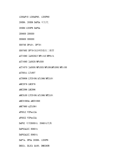
1200AP40 1200AP60、1203P60200D6、203D6 DAP8A 可互代203D6/1203P6 DAP8A2S0680 2S08803S0680 3S08805S0765 DP104、DP7048S0765C DP704加24V的稳压二极管ACT4060 ZA3020LV/MP1410/MP9141ACT4065 ZA3020/MP1580ACT4070 ZA3030/MP1583/MP1591MP1593/MP1430 ACT6311 LT1937ACT6906 LTC3406/AT1366/MP2104AMC2576 LM2576AMC2596 LM2596AMC3100 LTC3406/AT1366/MP2104AMC34063A AMC34063AMC7660 AJC1564AP8012 VIPer12AAP8022 VIPer22ADAP02 可用SG5841 /SG6841代换DAP02ALSZ SG6841DAP02ALSZ SG6841DAP7A、DP8A 203D6、1203P6DH321、DL321 Q100、DM0265RDM0465R DM/CM0565RDM0465R/DM0565R 用cm0565r代换(取掉4脚的稳压二极管)DP104 5S0765DP704 5S0765DP706 5S0765DP804 DP904FAN7601 LAF0001LD7552 可用SG6841代(改4脚电阻)LD7575PS 203D6改1脚100K电阻为24KOB2268CP OB2269CPOB2268CP SG6841改4脚100K电阻为20-47KOCP1451 TL1451/BA9741/SP9741/AP200OCP2150 LTC3406/AT1366/MP2104OCP2160 LTC3407OCP2576 LM2576OCP3601 MB3800OCP5001 TL5001OMC2596 LM2596/AP1501PT1301 RJ9266PT4101 AJC1648/MP3202PT4102 LT1937/AJC1896/AP1522/RJ9271/MP1540SG5841SZ SG6841DZ/SG6841DSM9621 RJ9621/AJC1642SP1937 LT1937/AJC1896/AP1522/RJ9271/MP1540STR-G5643D STR-G5653D、STR-G8653DTEA1507 TEA1533TEA1530 TEA1532对应引脚功能接入THX202H TFC719THX203H TFC718STOP246Y TOP247YVA7910 MAX1674/75 L6920 AJC1610VIPer12A VIPer22A[audio01]ICE2A165(1A/650V.31W);ICE2A265(2A/650V.52W);ICE2B0565(0.5A/650V.23W):ICE2B165(1A/650V.31W);ICE2B265(2A/650V.52W);ICE2A180(1A/800V.29W);ICE2A280(2A/800.50W).KA5H0365R, KA5M0365R, KA5L0365R, KA5M0365RN# u) t! u1 W1 B) R, PKA5L0365RN, KA5H0380R, KA5M0380R, KA5L0380R1、KA5Q1265RF/RT(大小两种体积)、KA5Q0765、FSCQ1265RT、KACQ1265RF、FSCQ0765RT、FSCQ1565Q这是一类的,这些型号的引脚功能全都一样,只是输出功率不一样。

©On-Bright Electronics Confidential - 1 - OB_DOC_DS_5800
GENERAL DESCRIPTION
OB2358 combines a dedicated current mode PWM controller with a high voltage power MOSFET. It is optimized for high performance, low standby power, and cost effective off-line flyback converter applications in sub 27W range. OB2358 offers complete protection coverage with automatic self-recovery feature including Cycle-by-Cycle current limiting (OCP), over load protection (OLP), VDD over voltage clamp and under voltage lockout (UVLO). Excellent EMI performance is achieved with On-Bright proprietary frequency shuffling technique together with soft switching control at the totem pole gate drive output. The tone energy at below 20KHZ is minimized in the
design and audio noise is eliminated during operation. OB2358 is offered in DIP8 package. FEATURES ■ Power on Soft Start Reducing MOSFET Vds
Stress
■ Frequency shuffling for EMI
■ Extended Burst Mode Control For Improved
Efficiency and Minimum Standby Power Design
■ Audio Noise Free Operation ■ Fixed 50KHZ Switching Frequency
■ Internal Synchronized Slope Compensation ■ Low VDD Startup Current and Low Operating Current ■ Leading Edge Blanking on Current Sense Input ■ Good Protection Coverage With Auto Self-Recovery o VDD Over Voltage Clamp and Under Voltage Lockout with Hysteresis (UVLO) o On-Bright Proprietary Line Input Compensated Cycle-by-Cycle Over-current Threshold Setting For Constant Output Power Limiting Over Universal Input Voltage Range. o Overload Protection (OLP). o Over voltage Protection(OVP) APPLICATIONS Offline AC/DC flyback converter for ■ AC/DC adaptor ■ PDA power supplies
■ Digital Cameras and Camcorder Adaptor ■ VCR, SVR, STB, DVD&DVCD Player SMPS ■ Set-Top Box Power ■ Auxiliary Power Supply for PC and Server ■ Open-frame SMPS TYPICAL APPLICATION
Output Power Table
230VAC±15% 85-265VAC
Product Open Frame 1 Open Frame 1
OB2358 27W 16W Notes:
1. Maximum practical continuous power in an open frame design with sufficient drain pattern as a heat sink, at 50 ambient.℃ 查询OB2358供应商。