RC-4;中文规格书,Datasheet资料
- 格式:pdf
- 大小:68.54 KB
- 文档页数:3
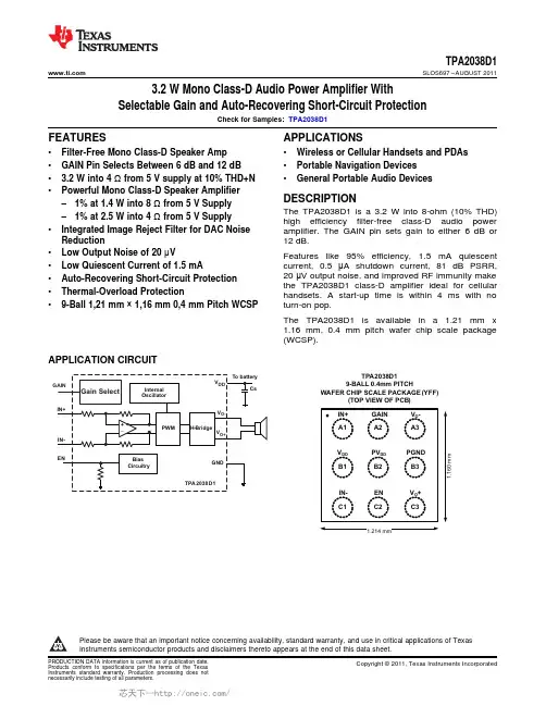
TPA2038D19-BALL0.4mm PITCHWAFER CHIP SCALE PACKAGE(YFF)(TOP VIEW OF PCB)TPA2038D1 SLOS697–AUGUST20113.2W Mono Class-D Audio Power Amplifier WithSelectable Gain and Auto-Recovering Short-Circuit ProtectionCheck for Samples:TPA2038D1FEATURES APPLICATIONS•Filter-Free Mono Class-D Speaker Amp•Wireless or Cellular Handsets and PDAs•GAIN Pin Selects Between6dB and12dB•Portable Navigation Devices• 3.2W into4Ωfrom5V supply at10%THD+N•General Portable Audio Devices•Powerful Mono Class-D Speaker AmplifierDESCRIPTION–1%at1.4W into8Ωfrom5V SupplyThe TPA2038D1is a3.2W into8-ohm(10%THD)–1%at2.5W into4Ωfrom5V Supply high efficiency filter-free class-D audio power•Integrated Image Reject Filter for DAC Noise amplifier.The GAIN pin sets gain to either6dB or Reduction12dB.•Low Output Noise of20μV Features like95%efficiency, 1.5mA quiescent•Low Quiescent Current of1.5mA current,0.5μA shutdown current,81dB PSRR,20μV output noise,and improved RF immunity make •Auto-Recovering Short-Circuit Protectionthe TPA2038D1class-D amplifier ideal for cellular •Thermal-Overload Protection handsets.A start-up time is within4ms with no•9-Ball1,21mm×1,16mm0,4mm Pitch WCSP turn-on pop.The TPA2038D1is available in a 1.21mm x1.16mm,0.4mm pitch wafer chip scale package(WCSP).APPLICATION CIRCUITPlease be aware that an important notice concerning availability,standard warranty,and use in critical applications of TexasInstruments semiconductor products and disclaimers thereto appears at the end of this data sheet.TPA2038D1SLOS697–These devices have limited built-in ESD protection.The leads should be shorted together or the device placed in conductive foam during storage or handling to prevent electrostatic damage to the MOS gates.ORDERING INFORMATIONT A PACKAGED DEVICES(1)PART NUMBER(2)SYMBOLTPA2038D1YFFR QWK -40°C to85°C9-ball WCSPTPA2038D1YFFT QWK(1)For the most current package and ordering information,see the Package Option Addendum at the end of this document,or see the TIWeb site at (2)The YFF package is only available taped and reeled.The suffix"R"indicates a reel of3000,the suffix"T"indicates a reel of250. ABSOLUTE MAXIMUM RATINGSover operating free-air temperature range,T A=25°C(unless otherwise noted)(1)VALUE UNITIn active mode–0.3to6.0VV DD,PV DD Supply voltageIn shutdown mode–0.3to6.0VV I Input voltage EN,IN+,IN––0.3to V DD+0.3VR L Minimum load resistance 3.2ΩOutput continuous total power dissipation See Dissipation Rating TableT A Operating free-air temperature range–40to85°CT J Operating junction temperature range–40to150°CT stg Storage temperature range–65to85°C (1)Stresses beyond those listed under absolute maximum ratings may cause permanent damage to the device.These are stress ratingsonly,and functional operation of the device at these or any other conditions beyond those indicated under recommended operating conditions is not implied.Exposure to Absolute Maximum Ratings conditions for extended periods may affect device reliability.DISSIPATION RATINGSPACKAGE DERATING FACTOR(1)T A<25°C T A=70°C T A=85°CYFF(WCSP) 4.2mW/°C525mW336mW273mW(1)Derating factor measure with high K board.RECOMMENDED OPERATING CONDITIONSMIN MAX UNIT V DD,Class-D supply voltage 2.5 5.5VPV DDV IH High-level input voltage EN,GAIN 1.3VV IL Low-level input voltage EN,GAIN0.35VV IC Common mode input voltage range V DD=2.5V,5.5V,CMRR≥49dB0.75V DD-1.1VT A Operating free-air temperature–4085°C GAIN SETTINGGAIN PIN GAIN SETTINGGND12dBVDD6dBTPA2038D1 SLOS697–AUGUST2011ELECTRICAL CHARACTERISTICSPVDD=VDD=3.6V,T A=25°C(unless otherwise noted)PARAMETER TEST CONDITIONS MIN TYP MAX UNIT Output offset voltage|V OS|VDD=2.5V to5.5V,GAIN=VDD15mV (measured differentially)|I IH|High-level EN input current VDD=5.5V,EN=GAIN=5.5V50μA|I IL|Low-level EN input current VDD=5.5V,EN=GAIN=0V1μAVDD=5.5V,no load 1.8 2.5I(Q)Quiescent current VDD=3.6V,no load 1.5 2.3mAVDD=2.5V,no load 1.3 2.1I(SD)Shutdown current EN=0.35V,VDD=3.6V0.12μAR O,SD Output impedance in EN=0.35V2kΩshutdown modef(SW)Switching frequency VDD=2.5V to5.5V250300350kHzA V Gain GAIN=0V11.51212.5dBGAIN=VDD 5.56 6.5R EN Resistance from EN to GND300kΩA V=6dB;EN=VDD150R IN Single-ended input resistance A V=12dB;EN=VDD75kΩEN=0.35V75 OPERATING CHARACTERISTICSPVDD=VDD=3.6V,A V=6dB,T A=25°C,R L=8Ω(unless otherwise noted)PARAMETER TEST CONDITIONS MIN TYP MAX UNITV DD=5V 3.24THD+N=10%,f=1kHz,V DD=3.6V 1.62WR L=4ΩV DD=2.5V0.70V DD=5V 2.57THD+N=1%,f=1kHz,V DD=3.6V 1.32WR L=4ΩV DD=2.5V0.57P O Output powerV DD=5V 1.80THD+N=10%,f=1kHz,V DD=3.6V0.91WR L=8ΩV DD=2.5V0.42V DD=5V 1.46THD+N=1%,f=1kHz,V DD=3.6V0.74WR L=8ΩV DD=2.5V0.33V DD=3.6V,Inputs AC A-weighting20Output voltage noise,A V=6dB grounded with CI =2μF,No weighting26f=20Hz to20kHzE NμV RMSA-weighting27 Output voltage noise,A V=12dBNo weighting36VDD=5.0V,P O=1.0W,f=1kHz,R L=8Ω0.12%VDD=3.6V,P O=0.5W,f=1kHz,R L=8Ω0.05%VDD=2.5V,P O=0.2W,f=1kHz,R L=8Ω0.05%THD+N Total harmonic distortion plus noiseVDD=5.0V,P O=2.0W,f=1kHz,R L=4Ω0.32%VDD=3.6V,P O=1.0W,f=1kHz,R L=4Ω0.11%VDD=2.5V,P O=0.4W,f=1kHz,R L=4Ω0.12%A V=6dB,Inputs AC grounded with C I=2μF,81200mV pp ripple,f=217HzPSRR AC power supply rejection ratio dBA V=12dB,Inputs AC grounded with82C I=2μF,200mV pp ripple,f=217HzTPA2038D1SLOS697–OPERATING CHARACTERISTICS(continued)PVDD=VDD=3.6V,A V=6dB,T A=25°C,R L=8Ω(unless otherwise noted)PARAMETER TEST CONDITIONS MIN TYP MAX UNIT CMRR Common mode rejection ratio A V=6dB,V IC=200mV PP,f=217Hz79dBA V=12dB,V IC=200mV PP,f=217Hz77T SU Startup time from shutdown4msV O+shorted to VDDV O–shorted to VDDI SC Short circuit protection threshold V O+shorted to GND2AV O–shorted to GNDV O+shorted to V O–T AR Overcurrent recovery time VDD=2.5V to5.5V100msTerminal FunctionsTERMINALI/O DESCRIPTIONNAME WCSP BALLIN+A1I Positive audio input.GAIN A2I Gain select.Set to GND for12dB;set to VDD for6dB.V O-A3O Negative audio output.VDD B1I Power supply terminal.Connect to PVDD using a direct connection.PVDD B2I Class-D output power supply.Connect to VDD using a direct connection.GND B3I Ground.IN–C1I Negative audio input.EN C2I Enable.Set to logic high to enable device.V O+C3O Positive audio output.FUNCTIONAL BLOCK DIAGRAMTPA2038D1 SLOS697–AUGUST2011TEST SETUP FOR GRAPHS1.C I was shorted for any common-mode input voltage measurement.All other measurements were taken with C I=0.1μF(unless otherwise noted).2.C S1=0.1μF is placed very close to the device.The optional C S2=10μF is used for datasheet graphs.3.The30kHz low-pass filter is required even if the analyzer has an internal low-pass filter.An RC low-pass filter(1kΩ,4700pF)is used on each output for the data sheet graphs.P O − Output Power − W η − E f f i c i e n c y − %0.00.20.40.60.81.01.21.41.61.82.00102030405060708090100P O − Output Power − Wη − E f f i c i e n c y − %0.00.20.40.60.81.01.21.41.61.82.00102030405060708090100P O − Output Power − W P D − P o w e r D i s s i p a t i o n − W0.00.40.8 1.2 1.6 2.00.00.10.20.30.40.5P O − Output Power − WP D − P o w e r D i s s i p a t i o n − W0.00.40.8 1.2 1.6 2.0 2.4 2.8 3.2 3.6 4.00.00.10.20.30.40.50.6P O − Output Power − WI D D − S u p p l y C u r r e n t − A0.00.20.40.60.81.01.21.41.61.82.02.22.42.62.83.03.23.43.6100m200m 300m 400m 500m 600m 700m 800m 900m1P O − Output Power − WI D D − S u p p l y C u r r e n t − A0.00.20.40.60.81.01.21.41.61.82.00100m200m300m400m500m600mTPA2038D1SLOS697–AUGUST 2011TYPICAL CHARACTERISTICSPVDD =VDD =3.6V,C I =0.1μF,C S1=0.1μF,C S2=10μF,T A =25°C,R L =8Ω(unless otherwise noted)EFFICIENCY EFFICIENCY vs OUTPUT POWERvs OUTPUT POWERFigure 1.Figure 2.POWER DISSIPATION POWER DISSIPATION vs OUTPUT POWERvs OUTPUT POWERFigure 3.Figure 4.SUPPLY CURRENT SUPPLY CURRENT vs OUTPUT POWERvs OUTPUT POWERFigure 5.Figure 6.V DD − Supply Voltage − V I D D − S u p p l y C u r r e n t − m A2.53.03.54.04.55.05.51.001.251.501.752.00V EN − EN Voltage − VI D D − S u p p l y C u r r e n t − n A0.00.10.20.30.40.5050100150200R L − Load Resistance − ΩP O − O u t p u t P o w e r − W48121620242832R L − Load Resistance − ΩP O − O u t p u t P o w e r − W4812162024283201234V DD − Supply Voltage − V2.53.03.54.04.55.0TPA2038D1SLOS697–AUGUST 2011TYPICAL CHARACTERISTICS (continued)PVDD =VDD =3.6V,C I =0.1μF,C S1=0.1μF,C S2=10μF,T A =25°C,R L =8Ω(unless otherwise noted)SUPPLY CURRENT SUPPLY CURRENT vs SUPPLY VOLTAGEvs EN VOLTAGEFigure 7.Figure 8.OUTPUT POWER OUTPUT POWER vs LOAD RESISTANCEvs LOAD RESISTANCEFigure 9.Figure 10.OUTPUT POWER vs SUPPLY VOLTAGEFigure 11.P O − Output Power − WT H D +N − T o t a l H a r m o n i c D i s t o r t i o n + N o i s e − %10m100m15P O − Output Power − W10m100m15f − Frequency − HzT H D +N −T o t a l H a r m o n i c D i s t o r t i o n + N o i s e − %201001k10k20k0.0010.010.1110f − Frequency − HzT H D +N− T o t a l H a r m o n i c D i s t o r t i o n + N o i s e − %201001k10k20k0.0010.010.1110f − Frequency − HzT H D +N− T o t a l H a r m o n i c D i s t o r t i o n + N o i s e − %201001k10k20k0.0010.010.1110f − Frequency − HzT H D +N− T o t a l H a r m o n i c D i s t o r t i o n + N o i s e − %201001k10k20k0.0010.010.1110TPA2038D1SLOS697–AUGUST 2011TYPICAL CHARACTERISTICS (continued)PVDD =VDD =3.6V,C I =0.1μF,C S1=0.1μF,C S2=10μF,T A =25°C,R L =8Ω(unless otherwise noted)THD +NOISETHD +NOISEvs OUTPUT POWER (6dB GAIN)vs OUTPUT POWER (6dB GAIN)Figure 12.Figure 13.THD +NOISETHD +NOISEvs FREQUENCY (6dB GAIN)vs FREQUENCY (6dB GAIN)Figure 14.Figure 15.THD +NOISETHD +NOISEvs FREQUENCY (6dB GAIN)vs FREQUENCY (6dB GAIN)Figure 16.Figure 17.f − Frequency − HzT H D +N − T o t a l H a r m o n i c D i s t o r t i o n + N o i s e − %201001k10k20k0.0010.010.1110f − Frequency − HzT H D +N − T o t a l H a r m o n i c D i s t o r t i o n + N o i s e − %201001k10k20k0.0010.010.1110P O − Output Power − WT H D +N − T o t a l H a r m o n i c D i s t o r t i o n + N o i s e − %10m100m15P O − Output Power − W10m100m15f − Frequency − HzT H D +N− T o t a l H a r m o n i c D i s t o r t i o n + N o i s e − %201001k10k20k0.0010.010.1110f − Frequency − HzT H D +N− T o t a l H a r m o n i c D i s t o r t i o n + N o i s e − %201001k10k20k0.0010.010.1110TPA2038D1SLOS697–AUGUST 2011TYPICAL CHARACTERISTICS (continued)PVDD =VDD =3.6V,C I =0.1μF,C S1=0.1μF,C S2=10μF,T A =25°C,R L =8Ω(unless otherwise noted)THD +NOISETHD +NOISEvs FREQUENCY (6dB GAIN)vs FREQUENCY (6dB GAIN)Figure 18.Figure 19.THD +NOISETHD +NOISEvs OUTPUT POWER (12dB GAIN)vs OUTPUT POWER (12dB GAIN)Figure 20.Figure 21.THD +NOISETHD +NOISEvs FREQUENCY (12dB GAIN)vs FREQUENCY (12dB GAIN)Figure 22.Figure 23.f − Frequency − HzT H D +N − T o t a l H a r m o n i c D i s t o r t i o n + N o i s e − %201001k10k20k0.0010.010.1110f − Frequency − HzT H D +N − T o t a l H a r m o n i c D i s t o r t i o n + N o i s e − %201001k10k20k0.0010.010.1110f − Frequency − HzT H D +N − T o t a l H a r m o n i c D i s t o r t i o n + N o i s e − %201001k10k20k0.0010.010.1110f − Frequency − HzT H D +N − T o t a l H a r m o n i c D i s t o r t i o n + N o i s e − %201001k10k20k0.0010.010.1110V IC − Common Mode Input Voltage − VP S R R − P o w e r S u p p l y R e j e c t i o n R a t i o − d B0.00.5 1.0 1.5 2.0 2.5 3.0 3.5 4.0 4.5 5.0−100−90−80−70−60−50−40−30−20−10f − Frequency − HzP S R R − P o w e r S u p p l y R e j e c t i o n R a t i o − d B201001k10k20k−100−90−80−70−60−50−40−30−20−10TPA2038D1SLOS697–AUGUST 2011TYPICAL CHARACTERISTICS (continued)PVDD =VDD =3.6V,C I =0.1μF,C S1=0.1μF,C S2=10μF,T A =25°C,R L =8Ω(unless otherwise noted)THD +NOISETHD +NOISEvs FREQUENCY (12dB GAIN)vs FREQUENCY (12dB GAIN)Figure 24.Figure 25.THD +NOISETHD +NOISEvs FREQUENCY (12dB GAIN)vs FREQUENCY (12dB GAIN)Figure 26.Figure 27.POWER SUPPLY REJECTION RATIOPOWER SUPPLY REJECTION RATIOvs COMMON MODE INPUT VOLTAGE (12dB GAIN)vs FREQUENCY (6dB GAIN)Figure 28.Figure 29.f − Frequency − HzP S R R − P o w e r S u p p l y R e j e c t i o n R a t i o − d B201001k10k20k−100−90−80−70−60−50−40−30−20−100V IC − Common Mode Input Voltage − VP S R R − P o w e r S u p p l y R e j e c t i o n R a t i o − d B0.00.51.01.52.02.53.03.54.04.55.0−100−90−80−70−60−50−40−30−20−10f − Frequency − HzP S R R − P o w e r S u p p l y R e j e c t i o n R a t i o − d B201001k10k20k−100−90−80−70−60−50−40−30−20−10f − Frequency − HzP S R R − P o w e r S u p p l y R e j e c t i o n R a t i o − d B201001k10k 20k−100−90−80−70−60−50−40−30−20−100V IC − Common Mode Input Voltage − VC M R R − C o m m o n M o d e R e j e c t i o n R a t i o − d B0.00.51.01.52.02.53.03.54.04.55.0−100−90−80−70−60−50−40−30−20−100f − Frequency − HzC M R R − C o m m o n M o d e R e j e c t i o n R a t i o − d B201001k10k20k−100−90−80−70−60−50−40−30−20−100TPA2038D1SLOS697–AUGUST 2011TYPICAL CHARACTERISTICS (continued)PVDD =VDD =3.6V,C I =0.1μF,C S1=0.1μF,C S2=10μF,T A =25°C,R L =8Ω(unless otherwise noted)POWER SUPPLY REJECTION RATIOPOWER SUPPLY REJECTION RATIO vs FREQUENCY (6dB GAIN)vs COMMON MODE INPUT VOLTAGEFigure 30.Figure 31.POWER SUPPLY REJECTION RATIOPOWER SUPPLY REJECTION RATIOvs FREQUENCY (12dB GAIN)vs FREQUENCY (12dB GAIN)Figure 32.Figure 33.COMMON MODE REJECTION RATIOCOMMON MODE REJECTION RATIOvs COMMON MODE INPUT VOLTAGE (6dB GAIN)vs FREQUENCY (6dB GAIN)Figure 34.Figure 35.V IC − Common Mode Input Voltage − VC M R R − C o m m o n M o d e R e j e c t i o n R a t i o − d B−100−90−80−70−60−50−40−30−20−100f − Frequency − HzC M R R − C o m m o n M o d e R e j e c t i o n R a t i o − dB201001k10k20k−100−90−80−70−60−50−40−30−20−100V 500 mV/divDDV 500V/div OUTm C1 - High 3.6 VC1 -Amplitude 500 mV C1 - Duty Cycle 20%G026t −Time −ms 0 2.557.51012.51517.52022.525V 500 mV/divDDV 500V/divOUTm C1 - High 3.6 VC1 -Amplitude 500 mV C1 - Duty Cycle 20%G026t −Time −ms0 2.557.51012.51517.52022.525f −Frequency −kHz V −O u t p u t V o l t ag e −d B VO V −S u p p l y V o l t a g e −d B VD D −200−175−175−150−150−125−125−100−100−75−75−50−500−25−2502.4G0274.87.29.61214.416.819.221.624f −Frequency −kHzV −O u t p u t V o l t a g e −d B VO V −S u p p l y V o l t a g e −d B VD D −200−175−175−150−150−125−125−100−100−75−75−50−500−25−2502.4G0274.87.29.61214.416.819.221.624TPA2038D1SLOS697–AUGUST 2011TYPICAL CHARACTERISTICS (continued)PVDD =VDD =3.6V,C I =0.1μF,C S1=0.1μF,C S2=10μF,T A =25°C,R L =8Ω(unless otherwise noted)COMMON MODE REJECTION RATIOCOMMON MODE REJECTION RATIOvs COMMON MODE INPUT VOLTAGE (12dB GAIN)vs FREQUENCY (12dB GAIN)Figure 36.Figure 37.GSM POWER SUPPLY REJECTIONGSM POWER SUPPLY REJECTIONvs TIME (6dB GAIN)vs TIME (12dB GAIN)Figure 38.Figure 39.GSM POWER SUPPLY REJECTIONGSM POWER SUPPLY REJECTION vs FREQUENCY (6dB GAIN)vs FREQUENCY (12dB GAIN)Figure 40.Figure 41.()C I I 1f 2πR C =()I I C 1C 2πR f =TPA2038D1SLOS697–AUGUST 2011APPLICATION INFORMATIONSHORT CIRCUIT AUTO-RECOVERYWhen a short-circuit event occurs,the TPA2038D1goes to shutdown mode and activates the integrated auto-recovery process whose aim is to return the device to normal operation once the short-circuit is removed.This process repeatedly examines (once every 100ms)whether the short-circuit condition persists,and returns the device to normal operation immediately after the short-circuit condition is removed.This feature helps protect the device from large currents and maintain a good long-term reliability.INTEGRATED IMAGE REJECT FILTER FOR DAC NOISE REJECTIONIn applications which use a DAC to drive Class-D amplifiers,out-of-band noise energy present at the DAC's image frequencies fold back into the audio-band at the output of the Class-D amplifier.An external low-pass filter is often placed between the DAC and the Class-D amplifier in order to attenuate this noise.The TPA2038D1has an integrated Image Reject Filter with a low-pass cutoff frequency of 130kHz,which significantly attenuates this noise.Depending on the system noise specification,the integrated Image Reject Filter may help eliminate external filtering,thereby saving board space and component cost.COMPONENT SELECTIONFigure 42shows the TPA2038D1typical schematic with differential inputs,while Figure 43shows the TPA2038D1with differential inputs and input capacitors.Figure 44shows the TPA2038D1with a single-ended input.Decoupling Capacitors (C S1,C S2)The TPA2038D1is a high-performance class-D audio amplifier that requires adequate power supply decoupling to ensure the efficiency is high and total harmonic distortion (THD)is low.For higher frequency transients,spikes,or digital hash on the line,a good low equivalent-series-resistance (ESR)ceramic capacitor C S1=0.1μF,placed as close as possible to the device V DD lead works best.Placing C S1close to the TPA2038D1is important for the efficiency of the class-D amplifier,because any resistance or inductance in the trace between the device and the capacitor can cause a loss in efficiency.For filtering lower-frequency noise signals,a 10μF or greater capacitor (C S2)placed near the audio power amplifier would also help,but it is not required in most applications because of the high PSRR of this device.Typically,the smaller the capacitor's case size,the lower the inductance and the closer it can be placed to the TPA2038D1.X5R and X7R dielectric capacitors are recommended for both C S1and C S2.Input Capacitors (C I )The TPA2038D1does not require input coupling capacitors if the design uses a differential source that is biased within the common-mode input voltage range.That voltage range is listed in the Recommended Operating Conditions table.If the input signal is not biased within the recommended common-mode input range,such as in needing to use the input as a high pass filter,shown in Figure 43,or if using a single-ended source,shown in Figure 44,input coupling capacitors are required.The same value capacitors should be used on both IN+and IN –for best pop performance.The 3dB high-pass cutoff frequency f C of the filter formed by the input coupling capacitor C I and the input resistance R I (typically 150k Ω)of the TPA2038D1is given by Equation 1:(1)The value of the input capacitor is important to consider as it directly affects the bass (low frequency)performance of the circuit.Speaker response may also be taken into consideration when setting the corner frequency using input capacitors.Solving for the input coupling capacitance,we get:(2)If the corner frequency is within the audio band,the capacitors should have a tolerance of ±10%or better,because any mismatch in capacitance causes an impedance mismatch at the corner frequency and below.DifferentialInputTPA2038D1SLOS697–AUGUST 2011For a flat low-frequency response,use large input coupling capacitors (0.1μF or larger).X5R and X7R dielectric capacitors are recommended.Figure 42.Typical TPA2038D1Application Schematic With DC-coupled Differential InputFigure 43.Figureq JA +1Derating Factor T A Max +T J Max *q JA P DmaxFerrite TPA2038D1SLOS697–AUGUST 2011EFFICIENCY AND THERMAL INFORMATIONThe maximum ambient operating temperature of the TPA2038D1depends on the load resistance,power supply voltage and heat-sinking ability of the PCB system.The derating factor for the YFF package is shown in the dissipation rating table.Converting this to θJA :(3)Given θJA (from the Package Dissipation ratings table),the maximum allowable junction temperature (from theAbsolute Maximum ratings table),and the maximum internal dissipation (from Power Dissipation vs Output Power figures)the maximum ambient temperature can be calculated with the following equation.Note that the units on these figures are Watts RMS.Because audio contains crest factors (ratio of peak power to RMS power)from 9–15dB,thermal limitations are not usually encountered.(4)The TPA2038D1is designed with thermal protection that turns the device off when the junction temperaturesurpasses 150°C to prevent damage to the IC.Note that the use of speakers less resistive than 4Ω(typ)is not advisable.Below 4Ω(typ)the thermal performance of the device dramatically reduces because of increased output current and reduced amplifier efficiency.The Absolute Maximum rating of 3.2Ωcovers the manufacturing tolerance of a 4Ωspeaker and speaker impedance decrease due to frequency.θJA is a gross approximation of the complex thermal transfer mechanisms between the device and its ambient environment.If the θJA calculation reveals a potential problem,a more accurate estimate should be made.WHEN TO USE AN OUTPUT FILTERDesign the TPA2038D1without an Inductor /Capacitor (LC)output filter if the traces from the amplifier to the speaker are short.Wireless handsets and PDAs are great applications for this class-D amplifier to be used without an output filter.The TPA2038D1does not require an LC output filter for short speaker connections (approximately 100mm long or less).A ferrite bead can often be used in the design if failing radiated emissions testing without an LC filter;and,the frequency-sensitive circuit is greater than 1MHz.If choosing a ferrite bead,choose one with high impedance at high frequencies,but very low impedance at low frequencies.The selection must also take into account the currents flowing through the ferrite bead.Ferrites can begin to loose effectiveness at much lower than rated current values.See the EVM User's Guide (SLOU298)for components used successfully by TI.Figure 45shows a typical ferrite-bead output filter.Figure 45.Typical Ferrite Chip Bead FilterTPA2038D1SLOS697– PRINTED CIRCUIT BOARD LAYOUTIn making the pad size for the WCSP balls,it is recommended that the layout use non-solder-mask-defined (NSMD)land.With this method,the solder mask opening is made larger than the desired land area,and the opening size is defined by the copper pad width.Figure46shows the appropriate diameters for a WCSP layout.nd Pattern Image and DimensionsSOLDER PAD SOLDER MASK COPPER STENCIL COPPER PAD STENCIL OPENING(6)(7) DEFINITIONS OPENING(5)THICKNESS THICKNESSNon-solder-mask-1oz max0.275mm x0.275mm Sq.0.23mm0.310mm0.1mm thickdefined(NSMD)(0.032mm)(rounded corners)1.Circuit traces from NSMD defined PWB lands should be75μm to100μm wide in the exposed area insidethe solder mask opening.Wider trace widths reduce device stand off and impact reliability.2.Best reliability results are achieved when the PWB laminate glass transition temperature is above theoperating the range of the intended application.3.Recommend solder paste is Type3or Type4.4.For a PWB using a Ni/Au surface finish,the gold thickness should be less0.5mm to avoid a reduction inthermal fatigue performance.5.Solder mask thickness should be less than20μm on top of the copper circuit pattern6.Best solder stencil performance is achieved using laser cut stencils with electro e of chemicallyetched stencils give inferior solder paste volume control.7.Trace routing away from WCSP device should be balanced in X and Y directions to avoid unintentionalcomponent movement due to solder wetting forces.yout SnapshotAn on-pad via is not required to route the middle ball B2(PV DD)of the TPA2038D1.Short ball B2(PV DD)to ball B1(V DD)and connect both to the supply trace as shown in Figure47.This simplifies board routing and saves manufacturing cost.TPA2038D1 SLOS697–AUGUST2011PACKAGE DIMENSIONSD EMax=1244µm Max=1190µmMin=1184µm Min=1130µmPACKAGE OPTION ADDENDUM6-Oct-2011Addendum-Page 1PACKAGING INFORMATIONOrderable Device Status(1)Package Type PackageDrawingPins Package QtyEco Plan(2)Lead/Ball Finish MSL Peak Temp (3)Samples (Requires Login)TPA2038D1YFFR ACTIVE DSBGA YFF 93000Green (RoHS & no Sb/Br)SNAGCU Level-1-260C-UNLIM TPA2038D1YFFTACTIVEDSBGAYFF9250Green (RoHS & no Sb/Br)SNAGCULevel-1-260C-UNLIM(1)The marketing status values are defined as follows:ACTIVE: Product device recommended for new designs.LIFEBUY: TI has announced that the device will be discontinued, and a lifetime-buy period is in effect.NRND: Not recommended for new designs. Device is in production to support existing customers, but TI does not recommend using this part in a new design.PREVIEW: Device has been announced but is not in production. Samples may or may not be available.OBSOLETE: TI has discontinued the production of the device.(2)Eco Plan - The planned eco-friendly classification: Pb-Free (RoHS), Pb-Free (RoHS Exempt), or Green (RoHS & no Sb/Br) - please check /productcontent for the latest availability information and additional product content details.TBD: The Pb-Free/Green conversion plan has not been defined.Pb-Free (RoHS): TI's terms "Lead-Free" or "Pb-Free" mean semiconductor products that are compatible with the current RoHS requirements for all 6 substances, including the requirement that lead not exceed 0.1% by weight in homogeneous materials. Where designed to be soldered at high temperatures, TI Pb-Free products are suitable for use in specified lead-free processes.Pb-Free (RoHS Exempt): This component has a RoHS exemption for either 1) lead-based flip-chip solder bumps used between the die and package, or 2) lead-based die adhesive used between the die and leadframe. The component is otherwise considered Pb-Free (RoHS compatible) as defined above.Green (RoHS & no Sb/Br): TI defines "Green" to mean Pb-Free (RoHS compatible), and free of Bromine (Br) and Antimony (Sb) based flame retardants (Br or Sb do not exceed 0.1% by weight in homogeneous material)(3)MSL, Peak Temp. -- The Moisture Sensitivity Level rating according to the JEDEC industry standard classifications, and peak solder temperature.Important Information and Disclaimer:The information provided on this page represents TI's knowledge and belief as of the date that it is provided. TI bases its knowledge and belief on information provided by third parties, and makes no representation or warranty as to the accuracy of such information. Efforts are underway to better integrate information from third parties. TI has taken and continues to take reasonable steps to provide representative and accurate information but may not have conducted destructive testing or chemical analysis on incoming materials and chemicals.TI and TI suppliers consider certain information to be proprietary, and thus CAS numbers and other limited information may not be available for release.In no event shall TI's liability arising out of such information exceed the total purchase price of the TI part(s) at issue in this document sold by TI to Customer on an annual basis.芯天下--/。
Document Number: 88625For technical questions within your region, please contact one of the following: High Voltage Glass Passivated RectifierGI250-1 thru GI250-4Vishay General SemiconductorFEATURES•Superectifier structure for high reliability application•Cavity-free glass-passivated junction •Low leakage current•High forward surge capability•Meets environmental standard MIL-S-19500•Solder dip 275 °C max. 10 s, per JESD 22-B106•AEC-Q101 qualified•Compliant to RoH S Directive 2002/95/EC and in accordance to WEEE 2002/96/ECTYPICAL APPLICATIONSFor use in rectification of high voltage power supplies,inverters, converters and freewheeling diodes application.MECHANICAL DATACase: DO-204AL, molded epoxy over glass bodyMolding compound meets UL 94 V-0 flammability rating Base P/N-E3 - RoHS compliant, commercial grade Base P/NHE3 - RoHS compliant, AEC-Q101 qualified Terminals: Matte tin plated leads, solderable per J-STD-002 and JESD 22-B102E3 suffix meets JESD 201 class 1A whisker test, HE3 suffix meets JESD 201 class 2 whisker test Polarity: Color band denotes cathode endPRIMARY CHARACTERISTICSI F(AV)0.25 A V RRM 1000 V to 4000 VI FSM 15 A I R 5.0 μA V F 3.5 V T J max.175 °CDO-204AL (DO-41)SUPERECTIFIER ®MAXIMUM RATINGS (T A = 25°C unless otherwise noted)PARAMETERSYMBOL GI250-1GI250-2GI250-3GI250-4UNIT Maximum repetitive peak reverse voltage V RRM 1000200030004000V Maximum RMS voltage V RMS 700140021002800V Maximum DC blocking voltageV DC 1000200030004000V Maximum average forward rectified current 0.375" (9.5 mm)lead length at T A = 75 °CI F(AV)0.25A Peak forward surge current 8.3 ms single half sine-wave superimposed on rated loadI FSM 15A Operating junction and storage temperature rangeT J , T STG- 65 to + 175°C For technical questions within your region, please contact one of the following:Document Number: 88625GI250-1 thru GI250-4Vishay General SemiconductorNote(1)Thermal resistance from junction to ambient at 0.375" (9.5 mm) lead length, P.C.B. mountedNote(1)AEC-Q101 qualifiedRATINGS AND CHARACTERISTICS CURVES(T A = 25 °C unless otherwise noted)Fig. 1 - Forward Current Derating Curve Fig. 2 - Maximum Non-repetitive Peak Forward Surge CurrentELECTRICAL CHARACTERISTICS (T A = 25°C unless otherwise noted)PARAMETERTEST CONDITIONS SYMBOLGI250-1GI250-2GI250-3GI250-4UNIT Maximum instantaneous forward voltage 0.25 AV F 3.5V Maximum DC reverse current at rated DC blocking voltage T A = 25 °C I R 5.0μA T A = 100 °C50Typical reverse recovery time I F = 0.5 A, I R = 1.0 A,I rr = 0.25 A t rr 2.0μs Typical junction capacitance4.0 V, 1 MHzC J3.0pFTHERMAL CHARACTERISTICS (T A = 25°C unless otherwise noted)PARAMETERSYMBOL GI250-1GI250-2GI250-3GI250-4UNIT Typical thermal resistanceR JA (1)130°C/WORDERING INFORMATION (Example)PREFERRED P/N UNIT WEIGHT (g)PREFERRED PACKAGE CODEBASE QUANTITYDELIVERY MODEGI250-4E3/540.33954550013" diameter paper tape and reelGI250-4E3/730.339733000Ammo pack packaging GI250-4HE3/54 (1)0.33954550013" diameter paper tape and reelGI250-4HE3/73 (1)0.339733000Ammo pack packagingDocument Number: 88625For technical questions within your region, please contact one of the following: GI250-1 thru GI250-4Vishay General SemiconductorFig. 3 - Typical Instantaneous Forward Characteristics Fig. 4 - Typical Reverse CharacteristicsFig. 5 - Typical Junction CapacitancePACKAGE OUTLINE DIMENSIONS in inches (millimeters)Legal Disclaimer Notice VishayDisclaimerALL PRODU CT, PRODU CT SPECIFICATIONS AND DATA ARE SU BJECT TO CHANGE WITHOU T NOTICE TO IMPROVE RELIABILITY, FUNCTION OR DESIGN OR OTHERWISE.Vishay Intertechnology, Inc., its affiliates, agents, and employees, and all persons acting on its or their behalf (collectively,“Vishay”), disclaim any and all liability for any errors, inaccuracies or incompleteness contained in any datasheet or in any other disclosure relating to any product.Vishay makes no warranty, representation or guarantee regarding the suitability of the products for any particular purpose or the continuing production of any product. To the maximum extent permitted by applicable law, Vishay disclaims (i) any and all liability arising out of the application or use of any product, (ii) any and all liability, including without limitation special, consequential or incidental damages, and (iii) any and all implied warranties, including warranties of fitness for particular purpose, non-infringement and merchantability.Statements regarding the suitability of products for certain types of applications are based on Vishay’s knowledge of typical requirements that are often placed on Vishay products in generic applications. Such statements are not binding statements about the suitability of products for a particular application. It is the customer’s responsibility to validate that a particular product with the properties described in the product specification is suitable for use in a particular application. Parameters provided in datasheets and/or specifications may vary in different applications and performance may vary over time. All operating parameters, including typical parameters, must be validated for each customer application by the customer’s technical experts. Product specifications do not expand or otherwise modify Vishay’s terms and conditions of purchase, including but not limited to the warranty expressed therein.Except as expressly indicated in writing, Vishay products are not designed for use in medical, life-saving, or life-sustaining applications or for any other application in which the failure of the Vishay product could result in personal injury or death. Customers using or selling Vishay products not expressly indicated for use in such applications do so at their own risk and agree to fully indemnify and hold Vishay and its distributors harmless from and against any and all claims, liabilities, expenses and damages arising or resulting in connection with such use or sale, including attorneys fees, even if such claim alleges that Vishay or its distributor was negligent regarding the design or manufacture of the part. Please contact authorized Vishay personnel to obtain written terms and conditions regarding products designed for such applications.No license, express or implied, by estoppel or otherwise, to any intellectual property rights is granted by this document or by any conduct of Vishay. Product names and markings noted herein may be trademarks of their respective owners.Material Category PolicyVishay Intertechnology, Inc. hereb y certifies that all its products that are identified as RoHS-Compliant fulfill the definitions and restrictions defined under Directive 2011/65/EU of The European Parliament and of the Council of June 8, 2011 on the restriction of the use of certain hazardous substances in electrical and electronic equipment (EEE) - recast, unless otherwise specified as non-compliant.Please note that some Vishay documentation may still make reference to RoHS Directive 2002/95/EC. We confirm that all the products identified as being compliant to Directive 2002/95/EC conform to Directive 2011/65/EU.Revision: 12-Mar-121Document Number: 91000分销商库存信息:VISHAY-GENERAL-SEMICONDUCTORGI250-1-E3/73GI250-2-E3/73GI250-4-E3/73 GI250-1-E3/54GI250-2-E3/54GI250-3-E3/54 GI250-4-E3/54GI250-2HE3/73GI250-4HE3/73 GI250-2HE3/54GI250-4HE3/54。
Polyphase Multifunction Energy Metering ICADE7854/ADE7858/ADE7868/ADE7878 Rev. EInformation furnished by Analog Devices is believed to be accurate and reliable. However, noresponsibility is assumed by Analog Devices for its use, nor for any infringements of patents or other rights of third parties that may result from its use. Specifications subject to change without notice. No license is granted by implication or otherwise under any patent or patent rights of Analog Devices. T rademarks and registered trademarks are the property of their respective owners. One Technology Way, P.O. Box 9106, Norwood, MA 02062-9106, U.S.A. Tel: 781.329.4700 Fax: 781.461.3113 ©2010–2011 Analog Devices, Inc. All rights reserved.FEATURESHighly accurate; supports EN 50470-1, EN 50470-3,IEC 62053-21, IEC 62053-22, and IEC 62053-23 standards Compatible with 3-phase, 3- or 4-wire (delta or wye), and other 3-phase servicesSupplies total (fundamental and harmonic) active, reactive (ADE7878, ADE7868, and ADE7858 only), and apparent energy, and fundamental active/reactive energy (ADE7878 only) on each phase and on the overall systemLess than 0.1% error in active and reactive energy over a dynamic range of 1000 to 1 at T A = 25°CLess than 0.2% error in active and reactive energy over a dynamic range of 3000 to 1 at T A = 25°CSupports current transformer and di/dt current sensors Dedicated ADC channel for neutral current input (ADE7868 and ADE7878 only)Less than 0.1% error in voltage and current rms over a dynamic range of 1000 to 1 at T A = 25°CSupplies sampled waveform data on all three phases and on neutral currentSelectable no load threshold levels for total and fundamental active and reactive powers, as well as for apparent powersLow power battery mode monitors phase currents for antitampering detection (ADE7868 and ADE7878 only) Battery supply input for missing neutral operationPhase angle measurements in both current and voltage channels with a typical 0.3° errorWide-supply voltage operation: 2.4 V to 3.7 VReference: 1.2 V (drift 10 ppm/°C typical) with external overdrive capabilitySingle 3.3 V supply40-lead lead frame chip scale package (LFCSP), Pb-free Operating temperature: −40°C to +85°CFlexible I2C, SPI, and HSDC serial interfaces APPLICATIONSEnergy metering systemsGENERAL DESCRIPTIONThe ADE7854/ADE7858/ADE7868/ADE7878 are high accuracy, 3-phase electrical energy measurement ICs with serial interfaces and three flexible pulse outputs. The ADE78xx devices incorporate second-order sigma-delta (Σ-Δ) analog-to-digital converters (ADCs), a digital integrator, reference circuitry, and all of the signal processing required to perform total (fundamental and harmonic) active, reactive (ADE7878, ADE7868, and ADE7858), and apparent energy measurement and rms calcu-lations, as well as fundamental-only active and reactive energy measurement (ADE7878) and rms calculations. A fixed function digital signal processor (DSP) executes this signal processing. The DSP program is stored in the internal ROM memory. The ADE7854/ADE7858/ADE7868/ADE7878 are suitable for measuring active, reactive, and apparent energy in various 3-phase configurations, such as wye or delta services, with both three and four wires. The ADE78xx devices provide system calibration features for each phase, that is, rms offset correction, phase calibration, and gain calibration. The CF1, CF2, and CF3 logic outputs provide a wide choice of power information: total active, reactive, and apparent powers, or the sum of the current rms values, and fundamental active and reactive powers.The ADE7854/ADE7858/ADE7868/ADE7878 contain wave-form sample registers that allow access to all ADC outputs. The devices also incorporate power quality measurements, such as short duration low or high voltage detections, short duration high current variations, line voltage period measurement, and angles between phase voltages and currents. Two serial interfaces, SPI and I2C, can be used to communicate with the ADE78xx. A dedicated high speed interface, the high speed data capture (HSDC) port, can be used in conjunction with I2C to provide access to the ADC outputs and real-time power information. The ADE7854/ADE7858/ADE7868/ADE7878 also have two interrupt request pins, IRQ0 and IRQ1, to indicate that an enabled interrupt event has occurred. For the ADE7868/ADE7878, three specially designed low power modes ensure the continuity of energy accumulation when the ADE7868/ADE7878 is in a tam-pering situation. See for a quick reference chart listing each part and its functions. The ADE78xx are available in the 40-lead LFCSP, Pb-free package.Table 1Table 1. Part ComparisonPart No. WATT VARIRMS,VRMS,andVA di/dtFundamentalWATT andVARTamperDetectand LowPowerModes ADE7878 Yes Yes Yes Yes Yes Yes ADE7868 Yes Yes Yes Yes No Yes ADE7858 Yes Yes Yes Yes No No ADE7854 Yes No Yes Yes No NoADE7854/ADE7858/ADE7868/ADE7878Rev. E | Page 2 of 96TABLE OF CONTENTSFeatures..............................................................................................1 Applications.......................................................................................1 General Description.........................................................................1 Revision History...............................................................................3 Functional Block Diagrams.............................................................4 Specifications.....................................................................................8 Timing Characteristics..............................................................11 Absolute Maximum Ratings..........................................................14 Thermal Resistance....................................................................14 ESD Caution................................................................................14 Pin Configuration and Function Descriptions...........................15 Typical Performance Characteristics...........................................17 Test Circuit......................................................................................19 Terminology....................................................................................20 Power Management........................................................................21 PSM0—Normal Power Mode (All Parts)................................21 PSM1—Reduced Power Mode (ADE7868, ADE7878 Only)21 PSM2—Low Power Mode (ADE7868, ADE7878 Only).......21 PSM3—Sleep Mode (All Parts)................................................22 Power-Up Procedure..................................................................24 Hardware Reset...........................................................................25 Software Reset Functionality....................................................25 Theory of Operation......................................................................26 Analog Inputs..............................................................................26 Analog-to-Digital Conversion..................................................26 Current Channel ADC...............................................................27 di/dt Current Sensor and Digital Integrator..............................29 Voltage Channel ADC...............................................................30 Changing Phase Voltage Datapath...........................................31 Power Quality Measurements...................................................32 Phase Compensation.................................................................37 Reference Circuit........................................................................39 Digital Signal Processor.............................................................39 Root Mean Square Measurement.............................................40 Active Power Calculation..........................................................44 Reactive Power Calculation—ADE7858, ADE7868, ADE7878 Only..............................................................................................49 Apparent Power Calculation.....................................................54 Waveform Sampling Mode.......................................................57 Energy-to-Frequency Conversion............................................57 No Load Condition....................................................................61 Checksum Register.....................................................................63 Interrupts.....................................................................................64 Serial Interfaces..........................................................................65 ADE7878 Evaluation Board......................................................72 Die Version..................................................................................72 Silicon Anomaly.............................................................................73 ADE7854/ADE7858/ADE7868/ADE7878 FunctionalityIssues............................................................................................73 Functionality Issues....................................................................73 Section 1. ADE7854/ADE7858/ADE7868/ADE7878Functionality Issues....................................................................74 Registers List...................................................................................75 Outline Dimensions.......................................................................93 Ordering Guide.. (93)ADE7854/ADE7858/ADE7868/ADE7878Rev. E | Page 3 of 96REVISION HISTORY4/11—Rev. D to Rev. EChanges to Input Clock FrequencyParameter, Table 2..............10 Changes to Current RMS Offset Compensation Section..........42 Changes to Voltage RMS Offset Compensation Section...........44 Changes to Note 2, Table 30...........................................................77 Changes to Address 0xE707, Table 33..........................................80 Changes to Table 45........................................................................87 Changes to Table 46........................................................................88 Changes to Bit Location 7:3, Default Value, Table 54.. (92)2/11—Rev. C to Rev. DChanges to Figure 1...........................................................................4 Changes to Figure 2...........................................................................5 Changes to Figure 3...........................................................................6 Changes to Figure 4...........................................................................7 Changes to Table 2............................................................................8 Changed SCLK Edge to HSCLK Edge, Table 5...........................13 Change to Current Channel HPF Section...................................28 Change to di/dt Current Sensor and Digital IntegratorSection..............................................................................................30 Changes to Digital Signal Processor Section...............................39 Changes to Figure 59......................................................................44 Changes to Figure 62......................................................................47 Changes to Figure 65......................................................................49 Changes to Figure 66......................................................................52 Changes to Line Cycle Reactive Energy Accumulation Mode Section and to Figure 67.................................................................53 No Load Detection Based On Total Active, Reactive Powers Section..............................................................................................61 Change to Equation 50...................................................................63 Changes to the HSDC Interface Section......................................70 Changes to Figure 87 and Figure 88.............................................71 Changes to Figure 89......................................................................72 Changes to Table 30 (77)11/10—Rev. B to Rev. CChange to Signal-to-Noise-and-Distortion Ratio, SINADParameter, Table 1.............................................................................9 Changes to Figure 18......................................................................18 Changes to Figure 22......................................................................19 Changes to Silicon Anomaly Section............................................72 Added Table 28 to Silicon Anomaly Section, RenumberedTables Sequentially..........................................................................73 8/10—Rev. A to Rev. BChanges to Figure 1..........................................................................4 Changes to Figure 2..........................................................................5 Changes to Figure 3..........................................................................6 Changes to Figure 4..........................................................................7 Change to Table 8............................................................................16 Changes to Power-Up Procedure Section....................................23 Changes to Equation 6 and Equation 7........................................33 Changes to Equation 17.................................................................43 Changes to Active Power Offset Calibration Section.................45 Changes to Figure 63......................................................................46 Changes to Reactive Power Offset Calibration Section.............49 Changes to Figure 82......................................................................65 Added Silicon Anomaly Section, Renumbered TablesSequentially (71)3/10—Rev. 0 to Rev. AAdded ADE7854, ADE7858, and ADE7878..................Universal Reorganized Layout...........................................................Universal Added Table 1, Renumbered Sequentially.....................................1 Added Figure 1, Renumbered Sequentially...................................3 Added Figure 2..................................................................................4 Added Figure 3..................................................................................5 Changes to Specifications Section..................................................7 Changes to Figure 9........................................................................14 Changes to Table 8..........................................................................14 Changes to Typical Performance Characteristics Section.........16 Changes to Figure 22......................................................................18 Changes to the Power Management Section...............................20 Changes to the Theory of Operation Section..............................25 Changes to Figure 31 and Figure 32.............................................27 Change to Equation 28...................................................................47 Changes to Figure 83......................................................................66 Changes to Figure 86......................................................................68 Changes to the Registers List Section...........................................72 Changes to Ordering Guide.. (91)2/10—Revision 0: Initial VersionADE7854/ADE7858/ADE7868/ADE7878Rev. E | Page 4 of 96FUNCTIONAL BLOCK DIAGRAMSR E S E TR E F C L K I C L K O U I A I A V A I B I B V B I C I C V C V S C L K/S C LS D AH S DA08510-204Figure 1. ADE7854 Functional Block DiagramADE7854/ADE7858/ADE7868/ADE7878Rev. E | Page 5 of 96R E S E TR E F C L K I C L K O U I A I A V A I B I B V B I C I C V C V S C L K/S C LS D AH S DA08510-203Figure 2. ADE7858 Functional Block DiagramADE7854/ADE7858/ADE7868/ADE7878Rev. E | Page 6 of 96R E S E TR E F C L K I C L K O U I A I A V A I B I B V B I C I C V C V S C L K/S C LS D AH S DAI N I N 08510-202Figure 3. ADE7868 Functional Block DiagramADE7854/ADE7858/ADE7868/ADE7878Rev. E | Page 7 of 96R E S E TR E F C L K I C L K O U I A I A V A I B I B V B I C I C V C V S C L K/S C LS D AH S DAI N I N 08510-201Figure 4. ADE7878 Functional Block DiagramADE7854/ADE7858/ADE7868/ADE7878Rev. E | Page 8 of 96SPECIFICATIONSVDD = 3.3 V ± 10%, AGND = DGND = 0 V , on-chip reference, CLKIN = 16.384 MHz, T MIN to T MAX = −40°C to +85°C. Table 2.Parameter 1, 2 Min Typ Max Unit Test Conditions/Comments ACCURACYActive Energy MeasurementActive Energy Measurement Error (per Phase)Total Active Power0.1%Over a dynamic range of 1000 to 1, PGA = 1, 2, 4; integrator off0.2 % Over a dynamic range of 3000 to 1, PGA = 1, 2, 4;integrator off0.1 % Over a dynamic range of 500 to 1, PGA = 8, 16;integrator onFundamental Active Power (ADE7878 Only) 0.1% Over a dynamic range of 1000 to 1, PGA = 1, 2, 4; integrator off 0.2 % Over a dynamic range of 3000 to 1, PGA = 1, 2, 4;integrator off0.1 % Over a dynamic range of 500 to 1, PGA = 8, 16;integrator onPhase Error Between Channels Line frequency = 45 Hz to 65 Hz, HPF on Power Factor (PF) = 0.8 Capacitive ±0.05 Degrees Phase lead 37° PF = 0.5 Inductive ±0.05 Degrees Phase lag 60° AC Power Supply Rejection VDD = 3.3 V + 120 mV rms/120 Hz, IPx = VPx =±100 mV rmsOutput Frequency Variation 0.01 % DC Power Supply Rejection VDD = 3.3 V ± 330 mV dc Output Frequency Variation 0.01 %Total Active Energy MeasurementBandwidth2 kHz REACTIVE ENERGY MEASUREMENT(ADE7858, ADE7868, AND ADE7878)Reactive Energy Measurement Error(per Phase)Total Active Power 0.1 % Over a dynamic range of 1000 to 1, PGA = 1, 2, 4;integrator off0.2 % Over a dynamic range of 3000 to 1, PGA = 1, 2, 4;integrator off0.1 % Over a dynamic range of 500 to 1, PGA = 8, 16;integrator onFundamental Active Power (ADE7878 Only) 0.1% Over a dynamic range of 1000 to 1, PGA = 1, 2, 4; integrator off 0.2 % Over a dynamic range of 3000 to 1, PGA = 1, 2, 4;integrator off0.1 % Over a dynamic range of 500 to 1, PGA = 8, 16;integrator onPhase Error Between Channels Line frequency = 45 Hz to 65 Hz, HPF on PF = 0.8 Capacitive ±0.05 Degrees Phase lead 37° PF = 0.5 Inductive ±0.05 Degrees Phase lag 60° AC Power Supply Rejection VDD = 3.3 V + 120 mV rms/120 Hz, IPx = VPx =±100 mV rmsOutput Frequency Variation 0.01 %ADE7854/ADE7858/ADE7868/ADE7878Rev. E | Page 9 of 96Parameter 1, 2Min Typ Max Unit Test Conditions/Comments DC Power Supply Rejection VDD = 3.3 V ± 330 mV dc Output Frequency Variation0.01% Total Reactive Energy Measurement Bandwidth2kHzRMS MEASUREMENTSI rms and V rms Measurement Bandwidth2 kHz I rms and V rms Measurement Error (PSM0 Mode)0.1 % Over a dynamic range of 1000 to 1, PGA = 1 MEAN ABSOLUTE VALUE (MAV)MEASUREMENT (ADE7868 AND ADE7878)I mav Measurement Bandwidth (PSM1 Mode)260 Hz I mav Measurement Error (PSM1 Mode) 0.5 % Over a dynamic range of 100 to 1, PGA = 1, 2, 4, 8 ANALOG INPUTSMaximum Signal Levels±500mV peakDifferential inputs between the following pins: IAP and IAN, IBP and IBN, ICP and ICN; single-ended inputs between the following pins: VAP and VN, VBP and VN, VCP and VN Input Impedance (DC)IAP , IAN, IBP , IBN, ICP , ICN, VAP , VBP , and VCP Pins 400 kΩVN Pin130 kΩADC Offset Error±2 mV PGA = 1, uncalibrated error, see the Terminology sectionGain Error±4 % External 1.2 V referenceWAVEFORM SAMPLINGSampling CLKIN/2048, 16.384 MHz/2048 = 8 kSPS Current and Voltage Channels See the Waveform Sampling Mode section Signal-to-Noise Ratio, SNR70 dB PGA = 1 Signal-to-Noise-and-Distortion Ratio, SINAD60 dB PGA = 1Bandwidth (−3 dB)2 kHz TIME INTERVAL BETWEEN PHASESMeasurement Error0.3 Degrees Line frequency = 45 Hz to 65 Hz, HPF on CF1, CF2, CF3 PULSE OUTPUTSMaximum Output Frequency 8 kHz WTHR = VARTHR = VATHR = PMAX = 33,516,139 Duty Cycle50%If CF1, CF2, or CF3 frequency > 6.25 Hz and CFDEN is even and > 1(1 + 1/CFDEN) × 50% If CF1, CF2, or CF3 frequency > 6.25 Hz andCFDEN is odd and > 1Active Low Pulse Width 80 ms If CF1, CF2, or CF3 frequency < 6.25 Hz Jitter 0.04 % For CF1, CF2, or CF3 frequency = 1 Hz andnominal phase currents are larger than 10% of full scaleREFERENCE INPUT REF IN/OUT Input Voltage Range 1.1 1.3 V Minimum = 1.2 V − 8%; maximum = 1.2 V + 8% Input Capacitance 10 pF ON-CHIP REFERENCE Nominal 1.207 V at the REF IN/OUT pin at T A = 25°C PSM0 and PSM1 Modes Reference Error ±2 mV Output Impedance 1.2 kΩ Temperature Coefficient 10 50 ppm/°C Maximum value across full temperature rangeof −40°C to +85°CADE7854/ADE7858/ADE7868/ADE78781 See the Typical Performance Characteristics section.2 See the Terminology section for a definition of the parameters.Rev. E | Page 10 of 96分销商库存信息:ANALOG-DEVICESADE7878ACPZ ADE7854ACPZ ADE7854ACPZ-RL ADE7858ACPZ-RL ADE7868ACPZ-RL ADE7878ACPZ-RL ADE7858ACPZ ADE7868ACPZ EVAL-ADE7878EBZ。
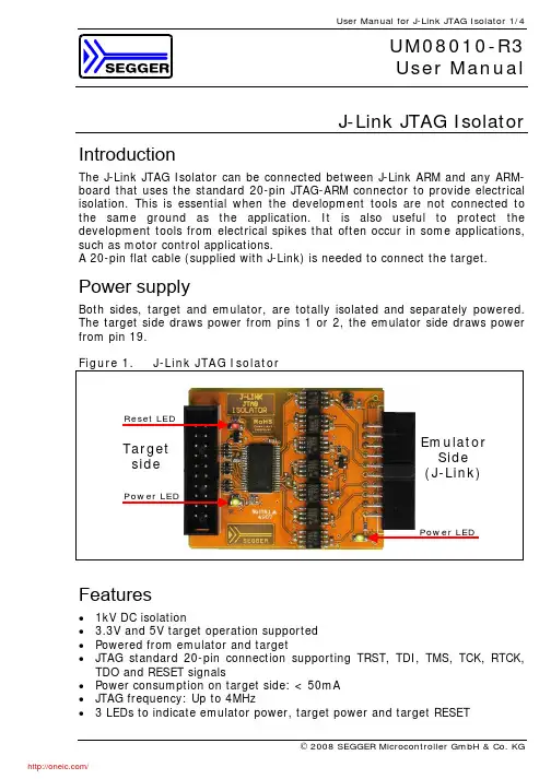
User Manual for J-Link JTAG Isolator 1/4© 2008 SEGGER Microcontroller GmbH & Co. KGUM08010-R3User Manual J-Link JTAG IsolatorIntroductionThe J-Link JTAG Isolator can be connected between J-Link ARM and any ARM-board that uses the standard 20-pin JTAG-ARM connector to provide electrical isolation. This is essential when the development tools are not connected to the same ground as the application. It is also useful to protect the development tools from electrical spikes that often occur in some applications, such as motor control applications.A 20-pin flat cable (supplied with J-Link) is needed to connect the target.Power supplyBoth sides, target and emulator, are totally isolated and separately powered. The target side draws power from pins 1 or 2, the emulator side draws power from pin 19.Figure 1. J-Link JTAG IsolatorPower LEDReset LEDPower LEDTarget sideEmulator Side (J-Link)Features• 1kV DC isolation• 3.3V and 5V target operation supported • Powered from emulator and target•JTAG standard 20-pin connection supporting TRST, TDI, TMS, TCK, RTCK, TDO and RESET signals• Power consumption on target side: < 50mA • JTAG frequency: Up to 4MHz• 3 LEDs to indicate emulator power, target power and target RESETUser Manual for J-Link JTAG Isolator 2/4© 2008 SEGGER Microcontroller GmbH & Co. KGConnectors and indicatorsThe Isolator uses high speed optocouplers that allow a very low propagation time between input and output. It comes with the following connectors and indicators:• 20-pin female EMULATOR connector which can be plugged directly into J-Link• 20-pin male TARGET connector for connection of the target cable • Green LED indicating power on the emulator side • Green LED indicating power on the target side • Red LED indicating RESETBlock diagramThe functional block diagram (Figure 2) illustrates the functional connections between the emulator and target.User Manual for J-Link JTAG Isolator 3/4© 2008 SEGGER Microcontroller GmbH & Co. KGConnecting the Isolator to Target and EmulatorTarget side is connected to the target via a 20-pin flat cable.Using the Isolator with J-LinkIn order to use the Isolator, follow these steps:• Plug the Isolator directly into J-Link. • Power J-Link.• Make sure the green LED on the emulator side is lit. If it is not, follow theinstruction in the next section.• Connect the target via 20-pin flat cable to the target side of the Isolator. • If the target is powered, the green LED on the target side should be lit.The red LED on the target side is lit when a Target RESET is active (low).Preparing J-Link to supply powerJ-Link needs to supply 5V power to the emulator side of the adapter on pin 19. In order to do this, you may have to configure J-Link once as follows: • Make sure that SEGGER J-Link software is installed on your machine.It can be downloaded from /download_jlink.html • Start J-Link Commander, which can be found under “Start -> Programs -> SEGGER -> J-Link ARM ”• Enter the following command: power on perm• Plug in the adapter: The LED on the emulator side should now be lit.Using the Isolator with an other ARM emulatorThe Isolator has been designed for J-Link, but can also be used with other ARM emulators with the same pin-out. In this case, you should make sure that 5V are supplied to pin 19 of the emulator connector and that your emulator is not damaged when applying 5V to this pin. Do this at your own risk!User Manual for J-Link JTAG Isolator 4/4© 2008 SEGGER Microcontroller GmbH & Co. KGDisclaimerSpecifications written in this document are believed to be accurate, but are not guaranteed to be entirely free of error. The information in this manual is subject to change for functional or performance improvements without notice. Please make sure your manual is the latest edition. While the information herein is assumed to be accurate, SEGGER Microcontroller GmbH & Co. KG (the manufacturer) assumes no responsibility for any errors or omissions. The manufacturer makes and you receive no warranties or conditions, express, implied, statutory or in any communication with you. The manufacturer specifically disclaims any implied warranty of merchantability or fitness for a particular purpose.Copyright noticeYou may not extract portions of this manual or modify the PDF file in any way without the prior written permission of the manufacturer.2008 SEGGER Microcontroller GmbH & Co. KG, Hilden / GermanyTrademarksNames mentioned in this manual may be trademarks of their respective companies.Brand and product names are trademarks or registered trademarks of their respective holders.Contact addressSEGGER Microcontroller GmbH & Co. KG In den Weiden 11 D-40721 Hilden GermanyTel.+49 2103-2878-0 Fax.+49 2103-2878-28Email: support@Internet: RevisionsRevision Date ByExplanation0 080104 OO Initial version1 080109 OO Added / updated picture for better understanding.2 080118 OO Updated Figure 2 “Functinal block diagram”3 080827 OO Minor changes分销商库存信息: SEGGER8.07.00 JTAG ISOLATOR。
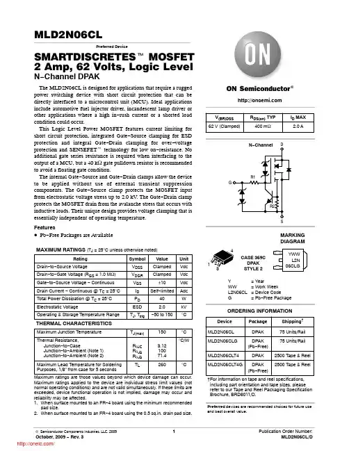
MLD2N06CLPreferred Device SMARTDISCRETES t MOSFET 2 Amp, 62 Volts, Logic Level N−Channel DPAKThe MLD2N06CL is designed for applications that require a rugged power switching device with short circuit protection that can be directly interfaced to a microcontrol unit (MCU). Ideal applications include automotive fuel injector driver, incandescent lamp driver or other applications where a high in−rush current or a shorted load condition could occur.This Logic Level Power MOSFET features current limiting for short circuit protection, integrated Gate−Source clamping for ESD protection and integral Gate−Drain clamping for over−voltage protection and SENSEFET t technology for low on−resistance. No additional gate series resistance is required when interfacing to the output of a MCU, but a 40 k W gate pulldown resistor is recommended to avoid a floating gate condition.The internal Gate−Source and Gate−Drain clamps allow the device to be applied without use of external transient suppression components. The Gate−Source clamp protects the MOSFET input from electrostatic voltage stress up to 2.0 kV. The Gate−Drain clamp protects the MOSFET drain from the avalanche stress that occurs with inductive loads. Their unique design provides voltage clamping that is essentially independent of operating temperature.Features•Pb−Free Packages are AvailableMAXIMUM RATINGS (T J = 25°C unless otherwise noted)Rating Symbol Value Unit Drain−to−Source Voltage V DSS Clamped Vdc Drain−to−Gate Voltage (R GS = 1.0 M W)V DGR Clamped Vdc Gate−to−Source Voltage − Continuous V GS±10Vdc Drain Current − Continuous @ T C = 25°C I D Self−limited Adc Total Power Dissipation @ T C = 25°C P D40W Electrostatic Voltage ESD 2.0kV Operating & Storage Temperature Range T J, T stg−50 to 150°C THERMAL CHARACTERISTICSMaximum Junction Temperature T J(max)150°CThermal Resistance,Junction−to−CaseJunction−to−Ambient (Note 1)Junction−to−Ambient (Note 2)R q JCR q JAR q JA3.1210071.4°C/WMaximum Lead Temperature for SolderingPurposes, 1/8″ from case for 5 secondsT L260°CMaximum ratings are those values beyond which device damage can occur. Maximum ratings applied to the device are individual stress limit values (not normal operating conditions) and are not valid simultaneously. If these limits are exceeded, device functional operation is not implied, damage may occur and reliability may be affected.1.When surface mounted to an FR−4 board using the minimum recommendedpad size.2.When surface mounted to an FR−4 board using the 0.5 sq.in. drain pad size.Device Package Shipping†ORDERING INFORMATIONMLD2N06CL DPAK75 Units/RailCASE 369CDPAKSTYLE 2MARKINGDIAGRAMY= YearWW= Work WeekL2N06CL= Device CodeG= Pb−Free PackagePreferred devices are recommended choices for future use and best overall value.S62 V (Clamped)400 m WR DS(on) TYP2.0 AI D MAXV(BR)DSS†For information on tape and reel specifications, including part orientation and tape sizes, please refer to our Tape and Reel Packaging Specification Brochure, BRD8011/D.MLD2N06CLT4DPAK2500 Tape & Reel MLD2N06CLT4G DPAK(Pb−Free)2500 Tape & Reel MLD2N06CLG DPAK(Pb−Free)75 Units/RailYWWL2N06CLGDRAIN −TO −SOURCE AVALANCHE CHARACTERISTICSRatingSymbol Value Unit Single Pulse Drain −to −Source Avalanche Energy (Starting T J = 25°C, I D = 2.0 A, L = 40 mH)E AS80mJELECTRICAL CHARACTERISTICS (T C = 25°C unless otherwise noted)CharacteristicSymbolMinTypMaxUnitOFF CHARACTERISTICSDrain −to −Source Breakdown Voltage (Internally Clamped)(I D = 20 mAdc, V GS = 0 Vdc)(I D = 20 mAdc, V GS = 0 Vdc, T J = 150°C)V (BR)DSS585862626666VdcZero Gate Voltage Drain Current (V DS = 40 Vdc, V GS = 0 Vdc)(V DS = 40 Vdc, V GS = 0 Vdc, T J = 150°C)I DSS −−0.66.0 5.020m AdcGate −Source Leakage Current (V G = 5.0 Vdc, V DS = 0 Vdc)(V G = 5.0 Vdc, V DS = 0 Vdc, T J = 150°C)I GSS −−0.51.05.020m AdcON CHARACTERISTICS (Note 3)Gate Threshold Voltage(I D = 250 m Adc, V DS = V GS )(I D = 250 m Adc, V DS = V GS , T J = 150°C)V GS(th)1.00.6 1.51.02.01.6VdcStatic Drain Current Limit(V GS = 5.0 Vdc, V DS = 10 Vdc)(V GS = 5.0 Vdc, V DS = 10 Vdc, T J = 150°C)I D(lim)3.81.64.42.45.22.9AdcStatic Drain −to −Source On −Resistance (I D = 1.0 Adc, V GS = 5.0 Vdc)(I D = 1.0 Adc, V GS = 5.0 Vdc, T J = 150°C)R DS(on)−−0.30.530.40.7WForward Transconductance (I D = 1.0 Adc, V DS = 10 Vdc)g FS 1.0 1.4−mhos Static Source −to −Drain Diode Voltage (I S = 1.0 Adc, V GS = 0 Vdc)V SD−1.11.5VdcRESISTIVE SWITCHING CHARACTERISTICS (Note 4)Turn −On Delay Time (V DD = 30 Vdc, I D = 1.0 Adc,V GS(on) = 5.0 Vdc, R GS = 25W )t d(on)− 1.0 1.5m sRise Timet r − 3.0 5.0Turn −Off Delay Time t d(off)− 5.08.0Fall Timet f−3.05.03.Pulse Test: Pulse Width ≤300 m s, Duty Cycle ≤ 2%.4.Switching characteristics are independent of operating junction temperature.Figure 1. Output Characteristics Figure 2. Transfer FunctionV DS , DRAIN-TO-SOURCE VOLTAGE (VOLTS)I D , D R A I N C U R R E N T (A M P S )I D , D R A I N C U R R E N T (A M P S )V GS , GATE-TO-SOURCE VOLTAGE (VOLTS)THE SMARTDISCRETES CONCEPTFrom a standard power MOSFET process, several active and passive elements can be obtained that provide on−chip protection to the basic power device. Such elements require only a small increase in silicon area and/or the addition of one masking layer to the process. The resulting device exhibits significant improvements in ruggedness and reliability as well as system cost reduction. The SMARTDISCRETES device functions can now provide an economical alternative to smart power ICs for power applications requiring low on−resistance, high voltage and high current.These devices are designed for applications that require a rugged power switching device with short circuit protection that can be directly interfaced to a microcontroller unit (MCU). Ideal applications include automotive fuel injector driver, incandescent lamp driver or other applications where a high in−rush current or a shorted load condition could occur. OPERATION IN THE CURRENT LIMIT MODEThe amount of time that an unprotected device can withstand the current stress resulting from a shorted load before its maximum junction temperature is exceeded is dependent upon a number of factors that include the amount of heatsinking that is provided, the size or rating of the device, its initial junction temperature, and the supply voltage. Without some form of current limiting, a shorted load can raise a device’s junction temperature beyond the maximum rated operating temperature in only a few milliseconds.Even with no heatsink, the MLD2N06CL can withstand a shorted load powered by an automotive battery (10 to 14 V) for almost a second if its initial operating temperature is under 100°C. For longer periods of operation in the current−limited mode, device heatsinking can extend operation from several seconds to indefinitely depending on the amount of heatsinking provided.SHORT CIRCUIT PROTECTION AND THE EFFECT OF TEMPERATUREThe on−chip circuitry of the MLD2N06CL offers an integrated means of protecting the MOSFET component from high in−rush current or a shorted load. As shown in the schematic diagram, the current limiting feature is provided by an NPN transistor and integral resistors R1 and R2. R2 senses the current through the MOSFET and forward biases the NPN transistor’s base as the current increases. As the NPN turns on, it begins to pull gate drive current through R1, dropping the gate drive voltage across it, and thus lowering the voltage across the gate−to−source of the power MOSFET and limiting the current. The current limit is temperature dependent as shown in Figure 3, and decreases from about 2.3 amps at 25°C to about 1.3 A at 150°C. Since the MLD2N06CL continues to conduct current and dissipate power during a shorted load condition, it is important to provide sufficient heatsinking to limit the device junction temperature to a maximum of 150°C. The metal current sense resistor R2 adds about 0.4 ohms to the power MOSFET’s on−resistance, but the effect of temperature on the combination is less than on a standard MOSFET due to the lower temperature coefficient of R2. The on−resistance variation with temperature for gate voltages of 4 and 5 V is shown in Figure 5.Back−to−back polysilicon diodes between gate and source provide ESD protection to greater than 2 kV, HBM. This on−chip protection feature eliminates the need for an external Zener diode for systems with potentially heavy line transients.Figure 3. I D(lim) VariationWith Temperature Figure 4. R DS(on) Variation WithGate −To −Source VoltageFigure 5. On −Resistance Variation WithTemperatureFigure 6. Maximum Avalanche Energyversus Junction Temperature Figure 7. Drain −Source Sustaining Voltage Variation With TemperatureI D (l i m ), D R A I N C U R R E N T (A M P S )T J , JUNCTION TEMPERATURE (°C)R D S (o n ), O N -R E S I S T A N C E (O H M S )V GS , GATE-TO-SOURCE VOLTAGE (VOLTS)12391045678R D S (o n ), O N -R E S I S T A N C E(O H M S )T J , JUNCTION TEMPERATURE (°C)- 50500100150T J , STARTING JUNCTION TEMPERATURE (°C)E A S , S I N G L E P U L S E D R A I N -T O -S O U R CE 255075100125150A V A L A N C H E E N E R G Y (m J )B V (D S S ), D R A I N -T O -S O U RC E S U S T A I N I N G V O L T A G E (V)T J = JUNCTION TEMPERATURE- 50015050100FORWARD BIASED SAFE OPERATING AREAThe FBSOA curves define the maximum drain −to −source voltage and drain current that a device can safely handle when it is forward biased, or when it is on, or being turned on. Because these curves include the limitations of simultaneous high voltage and high current, up to the rating of the device, they are especially useful to designers of linear systems. The curves are based on a case temperature of 25°C and a maximum junction temperature of 150°C. Limitations for repetitive pulses at various case temperatures can be determined by using the thermal response curves.ON Semiconductor Application Note, AN569, “Transient Thermal Resistance − General Data and Its Use” provides detailed instructions.MAXIMUM DC VOLTAGE CONSIDERATIONSThe maximum drain −to −source voltage that can be continuously applied across the MLD2N06CL when it is in current limit is a function of the power that must be dissipated. This power is determined by the maximum current limit at maximum rated operating temperature(1.8 A at 150°C) and not the R DS(on). The maximum voltage can be calculated by the following equation:V supply =(150 − T A )I D(lim) (R q JC + R q CA )where the value of R q CA is determined by the heatsink that is being used in the application.DUTY CYCLE OPERATIONWhen operating in the duty cycle mode, the maximum drain voltage can be increased. The maximum operating temperature is related to the duty cycle (DC) by the following equation:T C = (V DS x I D x DC x R q CA ) + T AThe maximum value of V DS applied when operating in a duty cycle mode can be approximated by:V DS =150 − T CI D(lim) x DC x R q JCFigure 8. Maximum Rated Forward Bias Safe Operating Area (MLD2N06CL)V DS , DRAIN-TO-SOURCE VOLTAGE (VOLTS), D R A I N C U R R E N T (A M P S )100101.00.1I D Figure 9. Thermal Response (MLD2N06CL)t, TIME (s)r (t ), N O R M A L I Z E D E F F E C T I V E T R A N S I E N T T H E R M A L R E S I S T A N C E0.010.11.01.0E - 051.0E - 041.0E - 031.0E - 02 1.0E - 011.0E+00 1.0E+01Figure 10. Switching Test CircuitFigure 11. Switching WaveformsACTIVE CLAMPINGSMARTDISCRETES technology can provide on−chip realization of the popular gate−to−source and gate−to−drain Zener diode clamp elements. Until recently, such features have been implemented only with discrete components which consume board space and add system cost. The SMARTDISCRETES technology approach economically melds these features and the power chip with only a slight increase in chip area.In practice, back−to−back diode elements are formed in a polysilicon region monolithicly integrated with, but electrically isolated from, the main device structure. Each back−to−back diode element provides a temperature compensated voltage element of about 7.2 V. As the polysilicon region is formed on top of silicon dioxide, the diode elements are free from direct interaction with the conduction regions of the power device, thus eliminating parasitic electrical effects while maintaining excellent thermal coupling.To achieve high gate−to−drain clamp voltages, several voltage elements are strung together; the MLD2N06CL uses 8 such elements. Customarily, two voltage elements are used to provide a 14.4 volt gate−to−source voltage clamp. For the MLD2N06CL, the integrated gate−to−source voltage elements provide greater than 2.0 kV electrostatic voltage protection.The avalanche voltage of the gate−to−drain voltage clamp is set less than that of the power MOSFET device. As soon as the drain−to−source voltage exceeds this avalanche voltage, the resulting gate−to−drain Zener current builds a gate voltage across the gate−to−source impedance, turning on the power device which then conducts the current. Since virtually all of the current is carried by the power device, the gate−to−drain voltage clamp element may be small in size. This technique of establishing a temperature compensated drain−to−source sustaining voltage (Figure 7) effectively removes the possibility of drain−to−source avalanche in the power device.The gate−to−drain voltage clamp technique is particularly useful for snubbing loads where the inductive energy would otherwise avalanche the power device. An improvement in ruggedness of at least four times has been observed when inductive energy is dissipated in the gate−to−drain clamped conduction mode rather than in the more stressful gate−to−source avalanche mode.TYPICAL APPLICATIONS: INJECTOR DRIVER, SOLENOIDS, LAMPS, RELAY COILSThe MLD2N06CL has been designed to allow directinterface to the output of a microcontrol unit to control anisolated load. No additional series gate resistance is required,but a 40k W gate pulldown resistor is recommended to avoida floating gate condition in the event of an MCU failure. Theinternal clamps allow the device to be used without anyexternal transistent suppressing components.MLD2N06CLPACKAGE DIMENSIONSDPAKCASE 369C −01ISSUE CVSUDIMMIN MAX MIN MAX MILLIMETERSINCHES A 0.2350.245 5.97 6.22B 0.2500.265 6.35 6.73C 0.0860.094 2.19 2.38D 0.0270.0350.690.88E 0.0180.0230.460.58F 0.0370.0450.94 1.14G 0.180 BSC 4.58 BSC H 0.0340.0400.87 1.01J 0.0180.0230.460.58K 0.1020.114 2.60 2.89L 0.090 BSC 2.29 BSC R 0.1800.215 4.57 5.45S 0.0250.0400.63 1.01U 0.020−−−0.51−−−V 0.0350.0500.89 1.27Z0.155−−−3.93−−−STYLE 2:PIN 1.GATE2.DRAIN3.SOURCE4.DRAINǒmm inchesǓSCALE 3:1*For additional information on our Pb −Free strategy and solderingdetails, please download the ON Semiconductor Soldering and Mounting Techniques Reference Manual, SOLDERRM/D.SOLDERING FOOTPRINT*ON Semiconductor and are registered trademarks of Semiconductor Components Industries, LLC (SCILLC). SCILLC reserves the right to make changes without further notice to any products herein. SCILLC makes no warranty, representation or guarantee regarding the suitability of its products for any particular purpose, nor does SCILLC assume any liability arising out of the application or use of any product or circuit, and specifically disclaims any and all liability, including without limitation special, consequential or incidental damages.“Typical” parameters which may be provided in SCILLC data sheets and/or specifications can and do vary in different applications and actual performance may vary over time. All operating parameters, including “Typicals” must be validated for each customer application by customer’s technical experts. SCILLC does not convey any license under its patent rights nor the rights of others. SCILLC products are not designed, intended, or authorized for use as components in systems intended for surgical implant into the body, or other applications intended to support or sustain life, or for any other application in which the failure of the SCILLC product could create a situation where personal injury or death may occur. Should Buyer purchase or use SCILLC products for any such unintended or unauthorized application, Buyer shall indemnify and hold SCILLC and its officers, employees, subsidiaries, affiliates,and distributors harmless against all claims, costs, damages, and expenses, and reasonable attorney fees arising out of, directly or indirectly, any claim of personal injury or death associated with such unintended or unauthorized use, even if such claim alleges that SCILLC was negligent regarding the design or manufacture of the part. SCILLC is an Equal Opportunity/Affirmative Action Employer. This literature is subject to all applicable copyright laws and is not for resale in any manner.SMARTDISCRETES and SENSEFET are trademarks of Semiconductor Components Industries, LLC (SCILLC).PUBLICATION ORDERING INFORMATION分销商库存信息:ONSEMIMLD2N06CLT4MLD2N06CLT4G。
1. General descriptionThe P89LPC933/934/935/936 is a single-chip microcontroller, available in low costpackages, based on a high performance processor architecture that executes instructions in two to four clocks, six times the rate of standard 80C51 devices. Many system-level functions have been incorporated into the P89LPC933/934/935/936 in order to reduce component count, board space, and system cost.2. Features and benefits2.1Principal features4kB/8kB/16kB byte-erasable flash code memory organized into 1kB/2 kB sectorsand 64-byte pages. Single-byte erasing allows any byte(s) to be used as non-volatile data storage.256-byte RAM data memory. Both the P89LPC935 and P89LPC936 also include a512-byte auxiliary on-chip RAM.512-byte customer data EEPROM on chip allows serialization of devices, storage ofsetup parameters, etc. (P89LPC935/936).Dual 4-input multiplexed 8-bit A/D converters/DAC outputs (P89LPC935/936, singleA/D on P89LPC933/934).Two analog comparators with selectable inputs and reference source.Two 16-bit counter/timers (each may be configured to toggle a port output upon timeroverflow or to become a PWM output) and a 23-bit system timer that can also be used as an RTC.Enhanced UART with fractional baud rate generator, break detect, framing errordetection, and automatic address detection; 400kHz byte-wide I 2C-bus communication port and SPI communication port.Capture/Compare Unit (CCU) provides PWM, input capture, and output comparefunctions (P89LPC935/936).High-accuracy internal RC oscillator option allows operation without external oscillatorcomponents. The RC oscillator option is selectable and fine tunable.2.4V to3.6V V DD operating range. I/O pins are 5V tolerant (may be pulled up ordriven to 5.5V).28-pin TSSOP , PLCC, and HVQFN packages with 23 I/O pins minimum and up to 26I/O pins while using on-chip oscillator and reset options.P89LPC933/934/935/9368-bit microcontroller with accelerated two-clock 80C51 core 4 kB/8 kB/16 kB 3 V byte-erasable flash with 8-bit ADCsRev. 8 — 12 January 2011Product data sheet2.2Additional featuresA high performance 80C51 CPU provides instruction cycle times of 111ns to 222nsfor all instructions except multiply and divide when executing at 18MHz. This is sixtimes the performance of the standard 80C51 running at the same clock frequency. Alower clock frequency for the same performance results in power savings and reduced EMI.Serial flash In-Circuit Programming (ICP) allows simple production coding with commercial EPROM programmers. Flash security bits prevent reading of sensitiveapplication programs.Serial flash In-System Programming (ISP) allows coding while the device is mounted in the end application.In-Application Programming (IAP) of the flash code memory. This allows changing the code in a running application.Watchdog timer with separate on-chip oscillator, requiring no external components.The watchdog prescaler is selectable from eight values.Low voltage reset (brownout detect) allows a graceful system shutdown when power fails. May optionally be configured as an interrupt.Idle and two different power-down reduced power modes. Improved wake-up from Power-down mode (a LOW interrupt input starts execution). Typical power-downcurrent is 1μA (total power-down with voltage comparators disabled).Active-LOW reset. On-chip power-on reset allows operation without external reset components. A reset counter and reset glitch suppression circuitry prevent spuriousand incomplete resets. A software reset function is also available.Configurable on-chip oscillator with frequency range options selected by user programmed flash configuration bits. Oscillator options support frequencies from20kHz to the maximum operating frequency of 18MHz.Oscillator fail detect. The watchdog timer has a separate fully on-chip oscillator allowing it to perform an oscillator fail detect function.Programmable port output configuration options: quasi-bidirectional, open drain, push-pull, input-only.Port ‘input pattern match’ detect. Port0 may generate an interrupt when the value of the pins match or do not match a programmable pattern.LED drive capability (20mA) on all port pins. A maximum limit is specified for the entire chip.Controlled slew rate port outputs to reduce EMI. Outputs have approximately 10ns minimum ramp times.Only power and ground connections are required to operate theP89LPC933/934/935/936 when internal reset option is selected.Four interrupt priority levels.Eight keypad interrupt inputs, plus two additional external interrupt inputs.Schmitt trigger port inputs.Second data pointer.Emulation support.3. Product comparison overviewTable 1 highlights the differences between the four devices. For a complete list of device features please see Section 2 “Features and benefits”.4. Ordering information4.1Ordering optionsTable 1.Product comparison overviewDeviceFlash memory Sector size ADC1ADC0CCU Data EEPROM P89LPC933 4 kB 1 kB X ---P89LPC9348 kB 1 kB X ---P89LPC9358 kB 1 kB X X X X P89LPC93616 kB2 kBXXXXTable 2.Ordering informationType number Package NameDescriptionVersion P89LPC935FA PLCC28plastic leaded chip carrier; 28 leads SOT261-2P89LPC933HDH TSSOP28plastic thin shrink small outlinepackage; 28leads; body width 4.4mmSOT361-1P89LPC933FDH P89LPC934FDH P89LPC935FDH P89LPC936FDH P89LPC935FHNHVQFN28plastic thermal enhanced very thin quad flat package; no leads;28terminals; body 6×6×0.85mmSOT788-1Table 3.Ordering optionsType number Flash memory Temperature range Frequency P89LPC933HDH 4 kB −40°C to +125°C 0MHz to 18MHzP89LPC933FDH 4kB −40°C to +85°CP89LPC935FA 8kBP89LPC934FDH P89LPC935FDH P89LPC935FHN P89LPC936FDH16kB5. Block diagram6. Pinning information6.1Pinning6.2Pin descriptionTable 4.Pin descriptionSymbol Pin Type DescriptionTSSOP28,PLCC28HVQFN28P0.0 to P0.7I/O Port0: Port0 is an 8-bit I/O port with a user-configurable output type.During reset Port0 latches are configured in the input only mode with theinternal pull-up disabled. The operation of Port0 pins as inputs andoutputs depends upon the port configuration selected. Each port pin isconfigured independently. Refer to Section 8.13.1 “Port configurations”and Table 11 “Static characteristics” for details.The Keypad Interrupt feature operates with Port0 pins.All pins have Schmitt trigger inputs.Port0 also provides various special functions as described below:P0.0/CMP2/ KBI0/AD01327I/O P0.0 — Port0 bit0.O CMP2 — Comparator2 output.I KBI0 — Keyboard input0.I AD01 — ADC0 channel 1 analog input. (P89LPC935/936)P0.1/CIN2B/ KBI1/AD102622I/O P0.1 — Port0 bit1.I CIN2B — Comparator2 positive input B.I KBI1 — Keyboard input1.I AD10 — ADC1 channel 0 analog input.P0.2/CIN2A/ KBI2/AD112521I/O P0.2 — Port0 bit2.I CIN2A — Comparator2 positive input A.I KBI2 — Keyboard input2.I AD11 — ADC1 channel 1 analog input.P0.3/CIN1B/ KBI3/AD122420I/O P0.3 — Port0 bit3.I CIN1B — Comparator1 positive input B.I KBI3 — Keyboard input3.I AD12 — ADC1 channel 2 analog input.P0.4/CIN1A/ KBI4/DAC1/ AD132319I/O P0.4 — Port0 bit4.I CIN1A — Comparator1 positive input A.I KBI4 — Keyboard input4.O DAC1 — Digital-to-analog converter output 1.I AD13 — ADC1 channel 3 analog input.P0.5/ CMPREF/ KBI52218I/O P0.5 — Port0 bit5.I CMPREF — Comparator reference (negative) input.I KBI5 — Keyboard input5.P0.6/CMP1/ KBI62016I/O P0.6 — Port0 bit6.O CMP1 — Comparator1 output.I KBI6 — Keyboard input6.P0.7/T1/ KBI71915I/O P0.7 — Port0 bit7.I/O T1 — Timer/counter1 external count input or overflow output.I KBI7 — Keyboard input7.P1.0 to P1.7I/O, I [1]Port1: Port1 is an 8-bit I/O port with a user-configurable output type,except for three pins as noted below. During reset Port1 latches areconfigured in the input only mode with the internal pull-up disabled. Theoperation of the configurable Port1 pins as inputs and outputs dependsupon the port configuration selected. Each of the configurable port pinsare programmed independently. Refer to Section 8.13.1 “Portconfigurations” and Table 11 “Static characteristics” for details. P1.2 andP1.3 are open drain when used as outputs. P1.5 is input only.All pins have Schmitt trigger inputs.Port1 also provides various special functions as described below:P1.0/TXD1814I/O P1.0 — Port1 bit0.O TXD — Transmitter output for the serial port.P1.1/RXD1713I/O P1.1 — Port1 bit1.I RXD — Receiver input for the serial port.P1.2/T0/SCL128I/O P1.2 — Port1 bit2 (open-drain when used as output).I/O T0 — Timer/counter0 external count input or overflow output (open-drainwhen used as output).I/O SCL — I2C serial clock input/output.P1.3/INT0/ SDA 117I/O P1.3 — Port1 bit3 (open-drain when used as output).I INT0 — External interrupt0 input.I/O SDA — I2C serial data input/output.P1.4/INT1106I P1.4 — Port1 bit4.I INT1 — External interrupt1 input.P1.5/RST62I P1.5 — Port1 bit5 (input only).I RST — External reset input during power-on or if selected via UCFG1.When functioning as a reset input, a LOW on this pin resets themicrocontroller, causing I/O ports and peripherals to take on their defaultstates, and the processor begins execution at address0. Also used duringa power-on sequence to force ISP mode. When using an oscillatorfrequency above 12MHz, the reset input function of P1.5 must beenabled. An external circuit is required to hold the device in reset atpower-up until VDD has reached its specified level. When systempower is removed VDD will fall below the minimum specifiedoperating voltage. When using an oscillator frequency above12MHz, in some applications, an external brownout detect circuitmay be required to hold the device in reset when VDD falls below theminimum specified operating voltage.P1.6/OCB51I/O P1.6 — Port1 bit6.O OCB — Output Compare B. (P89LPC935/936)P1.7/OCC/ AD00428I/O P1.7 — Port1 bit7.O OCC — Output Compare C. (P89LPC935/936)I AD00 — ADC0 channel 0 analog input. (P89LPC935/936)Table 4.Pin description …continuedSymbol Pin Type Description TSSOP28,PLCC28HVQFN28P2.0 to P2.7I/OPort 2: Port 2 is an 8-bit I/O port with a user-configurable output type. During reset Port 2 latches are configured in the input only mode with the internal pull-up disabled. The operation of Port 2 pins as inputs and outputs depends upon the port configuration selected. Each port pin is configured independently. Refer to Section 8.13.1 “Port configurations” and Table 11 “Static characteristics” for details.All pins have Schmitt trigger inputs.Port 2 also provides various special functions as described below:P2.0/ICB/ DAC0/AD03125I/O P2.0 — Port 2 bit 0.I ICB — Input Capture B. (P89LPC935/936)I DAC0 — Digital-to-analog converter output.IAD03 — ADC0 channel 3 analog input. (P89LPC935/936)P2.1/OCD/ AD02226I/O P2.1 — Port 2 bit 1.O OCD — Output Compare D. (P89LPC935/936)IAD02 — ADC0 channel 2 analog input. (P89LPC935/936)P2.2/MOSI 139I/O P2.2 — Port 2 bit 2.I/OMOSI — SPI master out slave in. When configured as master, this pin is output; when configured as slave, this pin is input.P2.3/MISO 1410I/O P2.3 — Port 2 bit 3.I/OMISO — When configured as master, this pin is input, when configured as slave, this pin is output.P2.4/SS 1511I/O P2.4 — Port 2 bit 4.I SS — SPI Slave select.P2.5/ SPICLK 1612I/O P2.5 — Port 2 bit 5.I/OSPICLK — SPI clock. When configured as master, this pin is output; when configured as slave, this pin is input. P2.6/OCA 2723I/O P2.6 — Port 2 bit 6.O OCA — Output Compare A. (P89LPC935/936)P2.7/ICA2824I/O P2.7 — Port 2 bit 7.IICA — Input Capture A. (P89LPC935/936)Table 4.Pin description …continuedSymbolPinTypeDescriptionTSSOP28, PLCC28HVQFN28[1]Input/output for P1.0 to P1.4, P1.6, P1.7. Input for P1.5.P3.0 to P3.1I/OPort 3: Port 3 is a 2-bit I/O port with a user-configurable output type.During reset Port 3 latches are configured in the input only mode with the internal pull-up disabled. The operation of Port 3 pins as inputs and outputs depends upon the port configuration selected. Each port pin is configured independently. Refer to Section 8.13.1 “Port configurations” and Table 11 “Static characteristics” for details.All pins have Schmitt trigger inputs.Port 3 also provides various special functions as described below:P3.0/XTAL2/ CLKOUT95I/O P3.0 — Port 3 bit 0.O XTAL2 — Output from the oscillator amplifier (when a crystal oscillator option is selected via the flash configuration.OCLKOUT — CPU clock divided by 2 when enabled via SFR bit (ENCLK - TRIM.6). It can be used if the CPU clock is the internal RC oscillator, watchdog oscillator or external clock input, except when XTAL1/XTAL2 are used to generate clock source for the RTC/system timer.P3.1/XTAL184I/O P3.1 — Port 3 bit 1.IXTAL1 — Input to the oscillator circuit and internal clock generator circuits (when selected via the flash configuration). It can be a port pin if internal RC oscillator or watchdog oscillator is used as the CPU clock source, and if XTAL1/XTAL2 are not used to generate the clock for the RTC/system timer.V SS 73I Ground: 0V reference.V DD2117IPower supply: This is the power supply voltage for normal operation as well as Idle and Power-down modes.Table 4.Pin description …continuedSymbolPinTypeDescriptionTSSOP28, PLCC28HVQFN287. Logic symbols8. Functional descriptionRemark: Please refer to the P89LPC933/934/935/936 User manual for a more detailedfunctional description.8.1Special function registersRemark: SFR accesses are restricted in the following ways:•User must not attempt to access any SFR locations not defined.•Accesses to any defined SFR locations must be strictly for the functions for the SFRs.•SFR bits labeled ‘-’, logic 0 or logic 1 can only be written and read as follows:–‘-’ Unless otherwise specified, must be written with logic 0, but can return anyvalue when read (even if it was written with logic 0). It is a reserved bit and may beused in future derivatives.–Logic 0 must be written with logic 0, and will return a logic 0 when read.–Logic 1 must be written with logic 1, and will return a logic 1 when read.P89LPC933_934_935_936All information provided in this document is subject to legal disclaimers.© NXP B.V. 2011. All rights reserved.Product data sheet Rev. 8 — 12 January 2011 13 of 77NXP Semiconductors P89LPC933/934/935/9368-bit microcontroller with accelerated two-clock 80C51 coreTable 5.Special function registers - P89LPC933/934* indicates SFRs that are bit addressable. Name Description SFR addr.Bit functions and addresses Reset valueMSB LSB Hex Binary Bit address E7E6E5E4E3E2E1E0ACC*Accumulator E0H 0000000000ADCON0A/D control register 08EH -----ENADC0--0000000000ADCON1A/D control register 197H ENBI1ENADCI 1TMM1EDGE1ADCI1ENADC1ADCS11ADCS100000000000ADINS A/D input select A3H ADI13ADI12ADI11ADI10----0000000000ADMODA A/D mode register A C0H BNDI1BURST1SCC1SCAN1----0000000000ADMODB A/D mode register B A1H CLK2CLK1CLK0-ENDAC1ENDAC0BSA1-00000x 0000AD0DAT3A/D_0 data register 3F4H 0000000000AD1BH A/D_1 boundary high register C4H FF 11111111AD1BL A/D_1 boundary low register BCH 0000000000AD1DAT0A/D_1 data register 0D5H 0000000000AD1DAT1A/D_1 data register 1D6H 0000000000AD1DAT2A/D_1 data register 2D7H 0000000000AD1DAT3A/D_1 data register 3F5H 0000000000AUXR1Auxiliary function register A2H CLKLP EBRR ENT1ENT0SRST 0-DPS 00[1]000000x0Bit address F7F6F5F4F3F2F1F0B* B register F0H 0000000000BRGR0Baud rate generator rate low BEH 00[2]00000000BRGR1Baud rate generator rate high BFH 00[1][2]00000000BRGCON Baudrate generator control BDH ------SBRGS BRGEN 00[2]xxxx xx00CMP1Comparator 1 control register ACH --CE1CP1CN1OE1CO1CMF100[1]xx000000CMP2Comparator 2 control register ADH --CE2CP2CN2OE2CO2CMF200[1]xx000000DIVM CPU clock divide-by-M control95H 0000000000DPTR Data pointer (2bytes)DPH Data pointer high 83H 0000000000DPL Data pointer low 82H 0000000000FMADRH Program flash address high E7H 0000000000芯天下--/P89LPC933_934_935_936All information provided in this document is subject to legal disclaimers.© NXP B.V. 2011. All rights reserved.Product data sheet Rev. 8 — 12 January 2011 14 of 77NXP Semiconductors P89LPC933/934/935/9368-bit microcontroller with accelerated two-clock 80C51 core FMADRL Program flash address low E6H 0000000000FMCON Program flash control (Read)E4H BUSY ---HVA HVE SV OI 7001110000Program flash control (Write)E4H FMCMD.7FMCMD.6FMCMD.5FMCMD.4FMCMD.3FMCMD.2FMCMD.1FMCMD.FMDATA Program flash data E5H 0000000000I2ADR I 2C slave address register DBH I2ADR.6I2ADR.5I2ADR.4I2ADR.3I2ADR.2I2ADR.1I2ADR.0GC 0000000000Bit address DF DE DD DC DB DA D9D8I2CON*I 2C control register D8H -I2EN STA STO SI AA -CRSEL 00x00000x0I2DAT I 2C data register DAHI2SCLH Serial clock generator/SCL duty cycle register highDDH 0000000000I2SCLL Serial clock generator/SCL duty cycle register lowDCH 0000000000I2STAT I 2C status register D9H STA.4STA.3STA.2STA.1STA.0000F811111000ICRAH Input capture A register high ABH 0000000000ICRAL Input capture A register low AAH 0000000000ICRBH Input capture B register high AFH 0000000000ICRBL Input capture B register low AEH 0000000000Bit address AF AE AD AC AB AA A9A8IEN0*Interrupt enable 0A8H EA EWDRT EBO ES/ESR ET1EX1ET0EX00000000000Bit address EF EE ED EC EB EA E9E8IEN1*Interrupt enable 1E8H EAD EST --ESPI EC EKBI EI2C 00[3]00x00000Bit address BF BE BD BC BB BA B9B8IP0*Interrupt priority 0B8H -PWDRT PBO PS/PSR PT1PX1PT0PX000[3]x0000000IP0H Interrupt priority 0 high B7H -PWDRT H PBOH PSH/ PSRHPT1H PX1H PT0H PX0H 00[3]x0000000Bit address FF FE FD FC FB FA F9F8IP1*Interrupt priority 1F8H PAD PST --PSPI PC PKBI PI2C 00[3]00x00000IP1H Interrupt priority 1 high F7H PADH PSTH --PSPIH PCH PKBIH PI2CH 00[3]00x00000Table 5.Special function registers - P89LPC933/934 …continued* indicates SFRs that are bit addressable.Name Description SFR addr.Bit functions and addresses Reset valueMSB LSB Hex Binary芯天下--/P89LPC933_934_935_936All information provided in this document is subject to legal disclaimers.© NXP B.V. 2011. All rights reserved.Product data sheet Rev. 8 — 12 January 2011 15 of 77NXP Semiconductors P89LPC933/934/935/9368-bit microcontroller with accelerated two-clock 80C51 core KBCON Keypad control register 94H ------PATN _SELKBIF 00[3]xxxx xx00KBMASK Keypad interrupt mask register 86H 0000000000KBPATN Keypad pattern register 93H FF 11111111Bit address 8786858483828180P0*Port 080H T1/KB7CMP1/KB6CMPREF /KB5CIN1A /KB4CIN1B /KB3CIN2A /KB2CIN2B /KB1CMP2/KB0[3]Bit address 9796959493929190P1*Port 190H --RST INT1INT0/ SDAT0/SCL RXD TXD [3]Bit address A7A6A5A4A3A2A1A0P2*Port 2A0H --SPICLK SS MISO MOSI --[3]Bit address B7B6B5B4B3B2B1B0P3*Port 3B0H ------XTAL1XTAL2[3]P0M1Port 0 output mode 184H (P0M1.7)(P0M1.6)(P0M1.5)(P0M1.4)(P0M1.3)(P0M1.2)(P0M1.1)(P0M1.0)FF [3]11111111P0M2Port 0 output mode 285H (P0M2.7)(P0M2.6)(P0M2.5)(P0M2.4)(P0M2.3)(P0M2.2)(P0M2.1)(P0M2.0)00[3]00000000P1M1Port 1 output mode 191H (P1M1.7)(P1M1.6)-(P1M1.4)(P1M1.3)(P1M1.2)(P1M1.1)(P1M1.0)D3[3]11x1xx11P1M2Port 1 output mode 292H (P1M2.7)(P1M2.6)-(P1M2.4)(P1M2.3)(P1M2.2)(P1M2.1)(P1M2.0)00[3]00x0xx00P2M1Port 2 output mode 1A4H (P2M1.7)(P2M1.6)(P2M1.5)(P2M1.4)(P2M1.3)(P2M1.2)(P2M1.1)(P2M1.0)FF [3]11111111P2M2Port 2 output mode 2A5H (P2M2.7)(P2M2.6)(P2M2.5)(P2M2.4)(P2M2.3)(P2M2.2)(P2M2.1)(P2M2.0)00[3]00000000P3M1Port 3output mode 1B1H ------(P3M1.1)(P3M1.0)03[3]xxxx xx11P3M2Port 3 output mode 2B2H ------(P3M2.1)(P3M2.0)00[3]xxxx xx00PCON Power control register 87H SMOD1SMOD0BOPD BOI GF1GF0PMOD1PMOD00000000000PCONA Power control register A B5H RTCPD -VCPD ADPD I2PD SPPD SPD -00[3]00000000Bitaddress D7D6D5D4D3D2D1D0PSW*Program status word D0H CY AC F0RS1RS0OV F1P 0000000000PT0AD Port 0 digital input disable F6H --PT0AD.5PT0AD.4PT0AD.3PT0AD.2PT0AD.1-00xx00000x RSTSRC Reset source register DFH --BOF POF R_BK R_WD R_SF R_EX [4]RTCCON Real-time clock control D1H RTCF RTCS1RTCS0---ERTC RTCEN 60[3][5]011x xx00Table 5.Special function registers - P89LPC933/934 …continued* indicates SFRs that are bit addressable.Name Description SFR addr.Bit functions and addresses Reset valueMSB LSB Hex Binary芯天下--/P89LPC933_934_935_936All information provided in this document is subject to legal disclaimers.© NXP B.V. 2011. All rights reserved.Product data sheet Rev. 8 — 12 January 2011 16 of 77NXP Semiconductors P89LPC933/934/935/9368-bit microcontroller with accelerated two-clock 80C51 core RTCH Real-time clock register high D2H 00[5]00000000RTCL Real-time clock register low D3H 00[5]00000000SADDR Serial port address register A9H 0000000000SADEN Serial port address enable B9H 0000000000SBUF Serial Port data buffer register 99H xx xxxx xxxxBit address 9F 9E 9D 9C 9B 9A 9998SCON*Serial port control 98H SM0/FE SM1SM2REN TB8RB8TI RI 0000000000SSTAT Serial port extended status registerBAH DBMOD INTLO CIDIS DBISEL FE BR OE STINT 0000000000SP Stack pointer 81H 0700000111SPCTL SPI control register E2H SSIG SPEN DORD MSTR CPOL CPHA SPR1SPR00400000100SPSTAT SPI status register E1H SPIF WCOL ------0000xx xxxx SPDAT SPI data register E3H 0000000000TAMOD Timer 0 and 1 auxiliary mode 8FH ---T1M2---T0M200xxx0xxx0Bit address 8F 8E 8D 8C 8B 8A 8988TCON*Timer 0 and 1 control 88H TF1TR1TF0TR0IE1IT1IE0IT00000000000TH0Timer 0 high 8CH 0000000000TH1Timer 1 high 8DH 0000000000TL0Timer 0 low 8AH 0000000000TL1Timer 1 low 8BH 0000000000TMOD Timer 0 and 1 mode 89H T1GATE T1C/T T1M1T1M0T0GATE T0C/T T0M1T0M00000000000TRIM Internal oscillator trim register 96H RCCLK ENCLK TRIM.5TRIM.4TRIM.3TRIM.2TRIM.1TRIM.0[6] [5]WDCON Watchdog control register A7H PRE2PRE1PRE0--WDRUN WDTOF WDCLK [7] [5]Table 5.Special function registers - P89LPC933/934 …continued* indicates SFRs that are bit addressable.Name Description SFR addr.Bit functions and addresses Reset valueMSB LSB Hex Binary芯天下--/P89LPC933_934_935_936All information provided in this document is subject to legal disclaimers.© NXP B.V. 2011. All rights reserved.Product data sheet Rev. 8 — 12 January 2011 17 of 77NXP Semiconductors P89LPC933/934/935/9368-bit microcontroller with accelerated two-clock 80C51 core[1]Unimplemented bits in SFRs (labeled ’-’) are X (unknown) at all times. Unless otherwise specified, ones should not be written to these bits since they may be used for otherpurposes in future derivatives. The reset values shown for these bits are logic 0s although they are unknown when read.[2]BRGR1 and BRGR0 must only be written if BRGEN in BRGCON SFR is logic 0. If any are written while BRGEN =1, the result is unpredictable.[3]All ports are in input only (high-impedance) state after power-up.[4]The RSTSRC register reflects the cause of the P89LPC933/934/935/936 reset. Upon a power-up reset, all reset source flags are cleared except POF and BOF; the power-on resetvalue is xx110000.[5]The only reset source that affects these SFRs is power-on reset.[6]On power-on reset, the TRIM SFR is initialized with a factory preprogrammed value. Other resets will not cause initialization of the TRIM register.[7]After reset, the value is 111001x1, i.e., PRE2 to PRE0 are all logic 1, WDRUN =1 and WDCLK =1. WDTOF bit is logic 1 after watchdog reset and is logic 0 after power-on reset.Other resets will not affect WDTOF.WDL Watchdog load C1H FF 11111111WFEED1Watchdog feed 1C2HWFEED2Watchdog feed 2C3HTable 5.Special function registers - P89LPC933/934 …continued* indicates SFRs that are bit addressable.Name Description SFR addr.Bit functions and addresses Reset valueMSB LSB Hex Binary芯天下--/P89LPC933_934_935_936All information provided in this document is subject to legal disclaimers.© NXP B.V. 2011. All rights reserved.Product data sheet Rev. 8 — 12 January 2011 18 of 77NXP Semiconductors P89LPC933/934/935/9368-bit microcontroller with accelerated two-clock 80C51 coreTable 6.Special function registers - P89LPC935/936* indicates SFRs that are bit addressable. Name Description SFR addr.Bit functions and addresses Reset valueMSB LSB Hex BinaryBit address E7E6E5E4E3E2E1E0ACC*Accumulator E0H 0000000000ADCON0A/D control register 08EH ENBI0ENADCI 0TMM0EDGE0ADCI0ENADC0ADCS01ADCS000000000000ADCON1A/D control register 197H ENBI1ENADCI 1TMM1EDGE1ADCI1ENADC1ADCS11ADCS100000000000ADINS A/D input select A3H ADI13ADI12ADI11ADI10ADI03ADI02ADI01ADI000000000000ADMODA A/D mode register A C0H BNDI1BURST1SCC1SCAN1BNDI0BURST0SCC0SCAN00000000000ADMODB A/D mode register B A1H CLK2CLK1CLK0-ENDAC1ENDAC0BSA1BSA000000x 0000AD0BH A/D_0 boundary high register BBH FF 11111111AD0BL A/D_0 boundary low register A6H 0000000000AD0DAT0A/D_0 data register 0C5H 0000000000AD0DAT1A/D_0 data register 1C6H 0000000000AD0DAT2A/D_0 data register 2C7H 0000000000AD0DAT3A/D_0 data register 3F4H 0000000000AD1BH A/D_1 boundary high register C4H FF 11111111AD1BL A/D_1 boundary low register BCH 0000000000AD1DAT0A/D_1 data register 0D5H 0000000000AD1DAT1A/D_1 data register 1D6H 0000000000AD1DAT2A/D_1 data register 2D7H 0000000000AD1DAT3A/D_1 data register 3F5H 0000000000AUXR1Auxiliary function register A2H CLKLP EBRR ENT1ENT0SRST 0-DPS 00000000x0Bit address F7F6F5F4F3F2F1F0B* B register F0H 0000000000BRGR0[2]Baud rate generator rate low BEH 0000000000BRGR1[2]Baud rate generator rate high BFH 0000000000BRGCON Baudrate generator control BDH ------SBRGS BRGEN 00[2]xxxx xx00CCCRA Capture compare A control registerEAH ICECA2ICECA1ICECA0ICESA ICNFA FCOA OCMA1OCMA00000000000芯天下--/P89LPC933_934_935_936All information provided in this document is subject to legal disclaimers.© NXP B.V. 2011. All rights reserved.Product data sheet Rev. 8 — 12 January 2011 19 of 77NXP Semiconductors P89LPC933/934/935/9368-bit microcontroller with accelerated two-clock 80C51 core CCCRB Capture compare B control registerEBH ICECB2ICECB1ICECB0ICESB ICNFB FCOB OCMB1OCMB00000000000CCCRC Capture compare C control register ECH -----FCOC OCMC1OCMC000xxxx x000CCCRD Capture compare D control registerEDH -----FCOD OCMD1OCMD000xxxx x000CMP1Comparator 1 control register ACH --CE1CP1CN1OE1CO1CMF100[3]xx000000CMP2Comparator 2 control register ADH --CE2CP2CN2OE2CO2CMF200[3]xx000000DEECON Data EEPROM control registerF1H EEIF HVERR ECTL1ECTL0---EADR80E 00001110DEEDAT Data EEPROM data register F2H 0000000000DEEADR Data EEPROM address registerF3H 0000000000DIVM CPU clock divide-by-M control95H 0000000000DPTR Data pointer (2bytes)DPH Data pointer high 83H 0000000000DPL Data pointer low 82H 0000000000FMADRH Program flash address high E7H 0000000000FMADRL Program flash address low E6H 0000000000FMCON Program flash control (Read)E4H BUSY ---HVA HVE SV OI 7001110000Program flash control (Write)E4H FMCMD.7FMCMD.6FMCMD.5FMCMD.4FMCMD.3FMCMD.2FMCMD.1FMCMD.FMDATA Program flash data E5H 0000000000I2ADR I 2C slave address register DBH I2ADR.6I2ADR.5I2ADR.4I2ADR.3I2ADR.2I2ADR.1I2ADR.0GC 0000000000Bitaddress DF DE DD DC DB DA D9D8I2CON*I 2C control register D8H -I2EN STA STO SI AA -CRSEL 00x00000x0I2DAT I 2C data register DAHI2SCLH Serial clock generator/SCL duty cycle register highDDH 0000000000Table 6.Special function registers - P89LPC935/936 …continued* indicates SFRs that are bit addressable.Name Description SFR addr.Bit functions and addresses Reset valueMSB LSB Hex Binary芯天下--/。

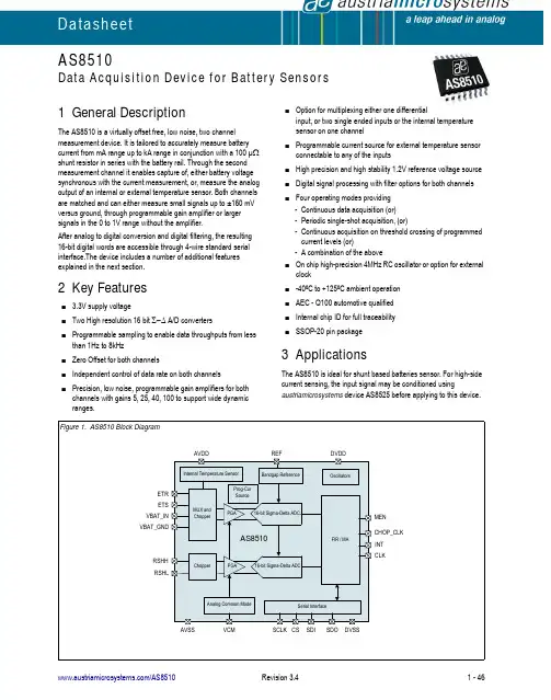
AS8510Data Acquisition Device for Battery SensorsDatasheet1 General DescriptionThe AS8510 is a virtually offset free, low noise, two channel measurement device. It is tailored to accurately measure battery current from mA range up to kA range in conjunction with a 100 µΩ shunt resistor in series with the battery rail. Through the second measurement channel it enables capture of, either battery voltage synchronous with the current measurement, or, measure the analog output of an internal or external temperature sensor. Both channels are matched and can either measure small signals up to ±160 mV versus ground, through programmable gain amplifier or larger signals in the 0 to 1V range without the amplifier.After analog to digital conversion and digital filtering, the resulting 16-bit digital words are accessible through 4-wire standard serial interface.The device includes a number of additional features explained in the next section.2 Key Features3.3V supply voltageTwo High resolution 16 bit Σ−Δ A/D convertersProgrammable sampling to enable data throughputs from lessthan 1Hz to 8kHzZero Offset for both channelsIndependent control of data rate on both channels Precision, low noise, programmable gain amplifiers for bothchannels with gains 5, 25, 40, 100 to support wide dynamic ranges.Option for multiplexing either one differentialinput, or two single ended inputs or the internal temperature sensor on one channelProgrammable current source for external temperature sensorconnectable to any of the inputsHigh precision and high stability 1.2V reference voltage source Digital signal processing with filter options for both channels Four operating modes providing-Continuous data acquisition (or)-Periodic single-shot acquisition, (or)-Continuous acquisition on threshold crossing of programmed current levels (or)-A combination of the aboveOn chip high-precision 4MHz RC oscillator or option for external clock-40ºC to +125ºC ambient operation AEC - Q100 automotive qualified Internal chip ID for full traceability SSOP-20 pin package3 ApplicationsThe AS8510 is ideal for shunt based batteries sensor. For high-side current sensing, the input signal may be conditioned usingaustriamicrosystems device AS8525 before applying to this device.Contents1 General Description (1)2 Key Features (1)3 Applications (1)4 Pin Assignments (4)4.1 Pin Descriptions (4)5 Absolute Maximum Ratings (6)6 Electrical Characteristics (7)6.1 Operating Conditions (7)6.2 DC/AC Characteristics for Digital Inputs and Outputs (7)6.3 Detailed System and Block Specifications (8)6.3.1 Electrical System Specifications (8)6.4 Current Measurement Ranges (across 100µΩ shunt resistor) (9)6.4.1 Differential Input Amplifier for Current Channel (10)6.4.2 Differential Input Amplifier for Voltage Channel (11)6.4.3 Sigma Delta Analog to Digital Converter (12)6.4.4 Bandgap Reference Voltage (12)6.4.5 Internal (Programmable) Current Source for External Temperature Measurement (13)6.4.6 CMREF Circuit (VCM) (14)6.4.7 Internal AVDD Power-on Reset (14)6.4.8 Internal DVDD Power-on Reset (14)6.4.9 Low Speed Oscillator (14)6.4.10 High Speed Oscillator (15)6.4.11 External Clock (15)6.4.12 Internal Temperature Sensor (15)6.5 System Specifications (16)7 Detailed Description (17)7.1 Current Measurement Channel (17)7.2 Voltage/Temperature Measurement Channel (17)7.3 Digital Implementation of Measurement Path (18)7.4 Modes of Operation (18)7.4.1 Normal Mode 1 (NOM1) (19)7.4.2 Normal Mode 2 (NOM2) (20)7.4.3 Standby Mode1 (SBM1) (21)7.4.4 Standby Mode2 (SBM2) (21)7.5 Reference-Voltage (22)7.6 Oscillators (22)7.7 Power-On Reset (22)7.8 4-Wire Serial Port Interface (22)7.8.1 SPI Frame (23)7.8.2 Write Command (23)7.8.3 Read Command (24)7.8.4 Timing (25)7.8.5 SPI Interface Timing (26)7.9 Control Register (27)7.9.1 Standby Mode - Power Consumption (38)7.9.2 Initialization Sequence at Power ON (38)7.9.3 Soft-reset Using Bit D[7] of Reset Register 0x09 (39)7.9.4 Reconfiguring Gain Setting of PGA (40)7.9.5 Configuring the Device During Normal Mode (40)7.10 Low Side Current Measurement Application (41)8 Package Drawings and Markings (42)8.1 Recommended PCB Footprint (43)9 Ordering Information (45)4 Pin AssignmentsFigure 2. Pin Assignments (Top View)4.1 Pin DescriptionsTable 1. Pin DescriptionsPin NumberPin Name Pin Type Description1RSHH Analog inputPositive Differential input for current channel 2RSHL Negative differential input for current channel3REFAnalog outputInternal reference voltage to sigma-delta ADC; connect 100nF to AVSS from this pin.4VCM Common Mode voltage to the internal measurement path; connect 100nF to AVSS from this pin.5AVDD Supply pad +3.3V Analog Power-supply 6AVSS 0V Power-supply analog 7ETR Analog input Voltage channel single ended input 8ETS 9VBAT_IN Battery voltage (high) input 10VBAT_GNDBattery voltage (low) input11CS Digital input with pull-up Chip select with an internal pull-up resistor (SPI Interface)12SCLK Digital input Clock signal (SPI Interface)13SDODigital outputSerial Data Input (SPI Interface)14DVSS Supply pad0V Digital Ground 15DVDD+3.3V Digital Supply16CHOP_CLKDigital outputChop Clock used in High side measurements to synchronize external chopper.(As an example, when AS8525 is used to condition the input signal to the input range of AS8510, the chop clock is used by AS8525.)17MENDigital output issued during the Standby Mode (SBM) to signal the short duration of data sampling. This signal is useful in the case of a High Side Measurement application.(For example: This signal is used by AS8525 device to wake-up and enable the measurement path.)18SDI Digital input Data signal (SPI Interface)19CLK Digital I/OBy default this pin is the internal clock output which can be used by a Microcontroller. The internal clock may also be disabled as an output by programming Register 08. To use an external Clock, Register 08 has to be programmed. 20INTDigital outputActive High Interrupt to indicate data is readyTable 1. Pin DescriptionsPin NumberPin Name Pin Type DescriptionDatasheet - A b s o lu t e M a x im u m R a ti n g s5 Absolute Maximum RatingsStresses beyond those listed in Table 2 may cause permanent damage to the device. These are stress ratings only. Functional operation of the device at these or any other conditions beyond those indicated in Electrical Characteristics on page 7 is not implied. Exposure to absolute maximum rating conditions for extended periods may affect device reliability.Table 2. Absolute Maximum RatingsParameter Min Max Units NotesElectrical ParametersDC supply voltage (AVDD and DVDD)-0.35VInput voltage (V IN)-0.3AVDD + 0.3DVDD + 0.3VInput current (latchup immunity)(I SCR)-100100mA AEC - Q100 - 004 Electrostatic DischargeElectrostatic discharge (ESD) all pins±2kV AEC - Q100 - 002 Continuous Power DissipationTotal power dissipation(all supplies and outputs) (P t)50mW SSOP20 in still air, soldered on JEDEC standard board @ 125º ambient, static operation with no time limitTemperature Ranges and Storage ConditionsStorage temperature (T STRG)-50125ºCJunction temperature (T J)130ºCThermal resistance (R thJC)80K/W JEDEC standard test board, 0 air velocityPackage body temperature (T BODY)260ºCNorm: IPC/JEDEC J-STD-020The reflow peak soldering temperature (body temperature) is specified according IPC/ JEDEC J-STD-020 “Moisture/Reflow Sensitivity Classification for Nonhermetic Solid StateSurface Mount Devices”.The lead finish for Pb-free leaded packages ismatte tin (100% Sn).Humidity non-condensing585%6 Electrical Characteristics6.1 Operating Conditions6.2 DC/AC Characteristics for Digital Inputs and OutputsAll pull-up and pull-down have been implemented with active devices. SDO has been measured with 10pF load.Table 3. Operating Conditions Symbol ParameterConditions Min Max Units AVDD Positive analog supply voltage3.0 3.6V AVSS 0V Ground00V A - D Difference in analog and digital supplies0.1V DVDD Positive digital supply 2.97 3.63V DVSS 0V Digital Ground 00V T AMB Ambient temperature -40125ºC I SUPP Supply current 5.5mA f CLKSystem clock frequency11.Nominal clock frequency from external or internal oscillator.4.096MHzTable 4. INTSymbol Parameter ConditionsMin TypMax Units I LEAK Tri-state leakage current -1+1µA V OH High level output voltage 2.5V V OL Low level output voltage0.4V I OOutput Current4mATable 5. CS InputSymbol Parameter ConditionsMin TypMaxUnits V IH High level input voltage 2.0V V IL Low level input voltage 0.8V I LEAK Input leakage current -1+1µA Ipu Pull up currentCS pulled to DV DD = 3.3V-150-15µATable 6. SDISymbol Parameter ConditionsMin TypMaxUnits V IH High level input voltage 2.0V V IL Low level input voltage 0.8V I LEAKInput leakage current-1+1µATable 7. SDO OutputSymbol Parameter Conditions Min Typ Max Units V OH High level output voltage Isource = 8mA 2.5V V OL Low level output voltage Isink = 8mA 0.4VI o Output Current8mA Table 8. CHOP_CLK OutputSymbol Parameter Conditions Min Typ Max Units V OH High level output voltage 2.5V V OL Low level output voltage0.4VI o Output Current4mA Table 9. CLK I/O with Input Schmitt Trigger and Output BufferSymbol Parameter Conditions Min Typ Max Units V IH High level input voltage DV DD = 3.3V 2.4V V IL Low level input voltage DV DD = 3.3V 1.0VI LEAK Input leakage current-1+1µAI PD Pull down current CLK pulled to DVSS10100µAI o Output Current4mAV OH High level output voltage 2.5V V OL Low level output voltage0.4V Table 10. SCLK with Input Schmitt TriggerSymbol Parameter Conditions Min Typ Max Units V IH High level input voltage DV DD = 3.3V 2.4V V IL Low level input voltage DV DD = 3.3V 1.0VI LEAK Input leakage current-1+1µA Table 11. MEN OutputSymbol Parameter Conditions Min Typ Max Units V OH High level output voltage 2.5V V OL Low level output voltage0.4VI O Output Current2mA6.3 Detailed System and Block Specifications6.3.1 Electrical System Specifications6.4 Current Measurement Ranges (across 100µΩ shunt resistor)Note:The Data Rate at the output can be calculated according to the formula:fsout=2*fchop /R2 (R2 is down sampling ratio taking values 1, 2, 4 up to 32768 as powers of 2)Table 12. Electrical System SpecificationsSymbol ParameterMinTyp Max Units NotesIDD NOM Current consumption normal mode 3 5.5mA IDD SBMCurrent consumption standby mode40µAAverage of NORMAL Mode Power consumption over a period of 10sec when the device is in STANDBY ModeTable 13. Current Measurement RangesSymbol ParameterImax [A]Vsh [mV]PGA Gain Nominal Data Rate (f OUT )V INADC 1[mV]1.V INADC = Vsh * Gain, gain deviations to be considered according to Table 15 and Table 16.PSR 2[dB]2.AVDD, DVDD of 3.3V with ±5% variation.I10 Input current range of 10A in NOM ±10±1100@ 1 kHz ±10060I200Input current range of 200A in NOM ±200±2040@ 1 kHz ±80060I400Input current range of 400A in NOM ±400±4025@ 1 kHz ±100060I1500Input current range of 1500A in NOM ±1500±1505@ 1 kHz ±75060I1Input current range of 1A in SBM33.For low power current monitoring, single shot measurement is performed with internal oscillator.±1±0.1100@ 1 Hz ±1060I10Input current range of 10A in SBM3±10±1100@ 1 Hz ±10060I200Input current range of 200A in SBM3±200±2040@ 1 Hz±80060Table 14. Valid Combinations of the Chopper Clock, Oversampling Clock and Decimation RatiosOver Sampling FrequencyChopper FrequencyDecimation Ratio1MHz 2kHz 642MHz 2kHz 642MHz 2kHz 1282MHz4kHz646.4.1 Differential Input Amplifier for Current ChannelNotes:1. Leakage test accuracy is limited by tester resource accuracy and tester hardware.2. For gain 100 PGA input common mode is 0V and the minimum supply is3.15V.3. The measurement ranges are referred only by the gain of input amplifier, while other parameters such as bandwidth etc. are pro-grammed independently.4. This parameter is not measured directly in production. It is measured indirectly via gain measurements of the whole path. It is guaran-teed by design.5. Pole frequency of input amplifier changes with GAIN. The number is valid for the gain at G1, while the bandwidth will be higher for other ranges. This parameter is not measured in production.6. Based on device evaluation. Not tested.7. These offsets are cancelled if chopping enabled (default).8. Noise density calculated by taking system bandwidth as 150Hz.9. Refer to Measurement Ranges shown in Table 13.10. No impact on the measurement path. If the chopping is enabled, both the offset and offset drift will be eliminated.11. For negative input voltages up to -160mV below ground, Input leakage is typically -20nA @ 65ºC due to forward conductance of protection diode.Table 15. Differential Input Amplifier for Current ChannelSymbol Parameter Conditions Min Typ Max Units V IN _AMP Input voltage range RSHH and RSHL-160+160mV I IN _AMP Input current1, 11RSHH and RSHL@ +160mV input voltage at 125ºC with PGA-50250nA ICM Absolute input voltage range2-160+300mVG = G1Gain1 3, 4, 9I10100G = G2Gain2 3, 4, 9I20040G = G3Gain3 3, 4, 9I40025G = G4Gain43, 4, 9I15005e Gain deviation i = 1, 2, 3, 40.9 * Gi 1.1 * Gif P _AMP Pole frequency4, 515kHzεT1Gain drift with temperature 6-20ºC to +65ºCGain 5, 25, referenced to roomtemperature±0.3%V OSDRIFT Offset drift with temperature 7, 10350µVVos Input referred offset7, 10After trim,for temperature range -20 to +65ºC350µV Vos_ch Chopping enabled0LSB VNdin Noise density4, 825nV/√Hz THD Total harmonic distortion For 150 Hz input signal 70dB分销商库存信息: AMSAS8510 DB。
Note: Some revisions of this device may incorporate deviations from published specifications known as errata. Multiple revisions of any device may be simultaneously available through various sales channels. For information about device errata, click here: /errata .FEATURES§ Two 32-bit counters keep track of real -time and elapsed time§ Counters keep track of seconds for over 125 years§ Battery powered counter counts seconds from the time battery is attached until V BAT is less than 2.5V§ V CC powered counter counts seconds while V CC is above V TP and retains the count in the absence of V CC under battery backup power § Clear function resets selected counter to 0 § Read/write serial port affords low pin count § Powered internally by a lithium energy cell that provides over 10 years of operation§ One-byte protocol defines read/write, counter address and software clear function§ Self-contained crystal provides an accuracy of ±2 min per month§ Operating temperature range of 0°C to +70°C § Low-profile SIP module§ Underwriters Laboratory (UL) recognized PIN ASSIGNMENTPIN DESCRIPTIONRST- Reset CLK - ClockDQ - Data Input/Output GND - Ground V CC - +5VOSC - 1Hz Oscillator Output NC- No ConnectDESCRIPTIONThe DS1603 is a real -time clock/elapsed time counter designed to count seconds when V CC power is applied and continually count seconds under battery backup power with an additional counter regardless of the condition of V CC . The continuous counter can be used to derive time of day, week, month, and year by using a software algorithm. The V CC powered counter will automatically record the amount of time that V CC power is applied. This function is particularly useful in determining the operational time of equipment in which the DS1603 is used. Alternatively, this counter can also be used under software control to record real -time events. Communication to and from the DS1603 takes place via a 3-wire serial port. A 1-byte protocol selects read/ write functions, counter clear functions and oscillator trim. The device contains a 32.768kHz crystal that will keep track of time to within ±2 min/mo. An internal lithium energy source contains enough energy to power the continuous seconds counter for over 10 years.OPERATIONThe main elements of the DS1603 are shown in Figure 1. As shown, communications to and from the elapsed time counter occur over a 3-wire serial port. The port is activated by driving RST to a high state.V CC RST DQ NC CLK OSC GND DS1603Elapsed Time Counter Moduleselect, register clear, and oscillator trim information. Each bit is serially input on the rising edge of the clock input. After the first eight clock cycles have loaded the protocol register with a valid protocol additional clocks will output data for a read or input data for a w rite. V CC must be present to access the DS1603. If V CC < V TP, the DS1603 will switch to internal power and disable the serial port to conserve energy. When running off of the internal power supply, only the continuous counter will continue to count and the counter powered by V CC will stop, but retain the count, which had accumulated when V CC power was lost. The 32-bit V CC counter is gated by V CC and the internal 1Hz signal.PROTOCOL REGISTERThe protocol bit definition is shown in Figure 2. Valid protocols and the resulting actions are shown in Table 1. Each data transfer to the protocol register designates what action is to occur. As defined, the MSB (bit 7 which is designated ACC) selects the 32-bit continuous counter for access. If ACC is a logical 1 the continuous counter is selected and the 32 clock cycles that follow the protocol will either read or write this counter. If the counter is being read, the contents will be latched into a different register at the end of protocol and the latched contents will be read out on the next 32 clock cycles. This avoids reading garbled data if the counter is clocked by the oscillator during a read. Similarly, if the counter is to be written, the data is buffered in a register and all 32 bits are jammed into the counter simultaneously on the rising edge of the 32nd clock. The next bit (bit 6 which is designated AVC) selects the 32–bit V CC active counter for access. If AVC is a logical 1 this counter is selected and the 32 clock cycles that follow will either read or write this counter. If both bit 7 and bit 6 are written to a logic high, all clock cycles beyond the protocol are ignored and bit 5, 4, and 3 are loaded into the oscillator trim register. A value of binary 3 (011) will give a clock accuracy of ±120 seconds per month at +25°C. Increasing the binary number towards 7 will cause the real-time clock to run faster. Conversely, lowering the binary number towards 0 will cause the clock to run slower. Binary 000 will stop the oscillator completely. This feature can be used to conserve battery life during storage. In this mode the internal power supply current is reduced to 100 nA maximum. In applications where oscillator trimming is not practical or not needed, a default setting of 011 is recommended. Bit 2 of protocol (designated CCC) is used to clear the continuous counter. When set to logic 1, the continuous counter will reset to 0 when RST is taken low. Bit 1 of protocol (designated CVC) is used to clear the V CC active counter. When set to logical 1, the V CC active counter will reset to 0 when RST is taken low. Both counters can be reset simultaneously by setting CCC and CVC both to a logical 1. Bit 0 of the protocol (designated RD) determines whether the 32 clocks to follow w ill write a counter or read a counter. When RD is set to a logical 0 a write action will follow when RD is set to a logical 1 a read action will follow. When sending the protocol, 8 bits should always be sent. Sending less than 8 bits can produce erroneous results. If clearing the counters or trimming the oscillator, the data transfer can be terminated after the 8-bit protocol is sent. However, when reading or writing the counters, 32 clock cycles should always follow the protocol.RESET AND CLOCK CONTROLAll data transfers are initiated by driving the RST input high. The RST input has two functions. First, RST turns on the serial port logic, which allows access to the protocol register for the protocol data entry. Second, the RST signal provides a method of terminating the protocol transfer or the 32-bit counter transfer. A clock cycle is a sequence of a rising edge followed by a falling edge. For write inputs, data must be valid during the rising edge of the clock. Data bits are output on the falling edge of the clock when data is being read. All data transfers terminate if the RST input is transitioned low and the DQ pin goes to a high-impedance state. RST should only be transitioned low while the clock is high to avoid disturbing the last bit of data. All data transfers must consist of 8 bits when transferring protocol only or 8 + 32 bits when reading or writing either counter. Data tran sfer is illustrated in Figure 3.DATA INPUTFollowing the 8-bit protocol that inputs write mode, 32 bits of data are written to the selected counter on the rising edge of the next 32 CLK cycles. After 32 bits have been entered any additional CLK cycles will be ignored until RST is transitioned low to end data transfer and then high again to begin new data transfer.DATA OUTPUTFollowing the eight CLK cycles that input read mode protocol, 32 bits of data will be output from the selected counter on the next 32 CLK cycles. The first data bit to be transmitted from the selected 32-bit counter occurs on the falling edge after the last bit of protocol is written. When transmitting data from the selected 32-bit counter, RST must remain at high level as a transition to low level will terminate data transfer. Data is driven out the DQ pin as long as CLK is low. When CLK is high the DQ pin is tristated. OSCILLATOR OUTPUTPin 6 of the DS1603 module is a 1Hz output signal. This signal is present only when V CC is applied and greater than the internal power supply. However, the output is guaranteed to meet TTL requirement only while V CC is within normal limits. This output can be used as a 1-second interrupt or time tick needed in some applications.INTERNAL POWERThe internal battery of the DS1603 module provides 35mAh and will run the elapsed time counter for over 10 years in the absence of power.PIN DESCRIPTIONSV CC, GND – DC power is provided to the device on these pins. V CC is the +5V input. When 5V is applied within normal limits, the device is fully accessible and data can be written and read. When a 3V battery is connected to the device and V CC is below 1.25 x V BAT, reads and writes are inhibited. As V CC falls below V BAT the continuous counter is switched over to the internal battery.CLK (Serial Clock Input) – CLK is used to synchronize data movement on the serial interface.DQ (Data Input/Output) – The DQ pin is the bi-directional data pin for the 3-wire interface.RST (Reset) – The reset signal must be asserted high during a read or a write.OSC (One Hertz Output Signal) – This signal is only present when Vcc is at a valid level and the oscillator is enabled.Figure 1. ELAPSED TIME COUNTER BLOCK DIAGRAMFigure 2. PROTOCOL BIT MAP7 6 5 4 3 2 1 0ACC AVC OSC2 OSC1 OSC0 CCC CVC RDTable 1. VALID PROTOCOLSPROTOCOLACTIONACC AVC OSC2 OSC1 OSC0 CCC CVC RDFUNCTION ReadContinuous Counter 1 0 X X X X X 1Output continuouscounter on the 32 clocksfollowing protocol.Oscillator trim registeris not updated. Countersare not reset.WriteContinuous Counter 1 0 X X X X X 0Input data to continuouscounter on the 32 clocksfollowing protocol.Oscillator trim registeris not updated. Countersare not reset.Read V CCActive Counter 0 1 X X X X X 1Output V CC activecounter on the 32 clocksfollowing protocol,oscillator trim registeris not updated. Countersare not reset.Write V CCActive Counter 0 1 X X X X X 0Input data to continuouscounter on the 32 clocksfollowing protocol.Oscillator trim registeris not updated. Countersare not reset.ClearContinuous Counter 0 0 X X X 1 X XResets the continuouscounter to all zeros atthe end of protocol.Oscillator trim registeris not updated.Clear V CCActive Counter 0 0 X X X X 1 XResets the V CC activecounter to all zeros atthe end of protocol.Oscillator trim registeris not updated.Set Oscillator Trim Bits 1 1 A B C X X 0Sets the oscillator trimregister to a value ofABC. Counters areunaffected.X = Don’t CareFigure 3. DATA TRANSFERTIMING DIAGRAM: READ/WRITE DATA TRANSFERNote: t CL, t CH, t R, and t F apply to both read and write data transfer.ABSOLUTE MAXIMUM RATINGSVoltage Range on Any Pin Relative to Ground -0.3V to +7.0VOperating Temperature Range 0°C to +70°CStorage Temperature Range -40°C to +70°CSoldering Temperature Range See IPC/JEDEC J-STD-020A (See Note 11)This is a stress rating only and functional operation of the device at these or any other conditions beyond t h ose indicated in the operation sections of this specification is not implied. Exposure to absolute maximum rating conditions for extended periods of time can affect reliability.RECOMMENDED DC OPERATING CONDITIONS (0°C to +70°C) PARAMETER SYMBOL MIN TYP MAX UNITS NOTES Supply Voltage V CC 4.5 5.0 5.5 V 1 Logic 1 Input V IH 2.0 V CC + 0.3 V 1 Logic 0 Input V IL-0.3 0.8 V 1DC ELECTRICAL CHARACTERISTICS (0°C to +70°C; V CC = 5V ±10%) PARAMETER SYMBOL MIN TYP MAX UNITS NOTES Input Leakage I LI-1 +1 µAI/O Leakage I LO-1 +1 µALogic 1 Output V OH 2.4 V 2 Logic 0 Output V OL0.4 V 3 Active Supply Current I CC 1 mA 4 Timekeeping Current I CC150 µA 5 Battery Trip Point V TP 3.0 4.5 V 9 CAPACITANCE (T A = +25°C) PARAMETER SYMBOL MIN TYP MAX UNITS NOTES Input Capacitance C I 5 pFI/O Capacitance C I/O10 pF(T A = +25°C) PARAMETER SYMBOL MIN TYP MAX UNITS NOTES Expected Datat DR10 years 10 Retention TimeNOTES:1) All voltages are referenced to ground.2) Logic 1 voltages are specified at a source current of 1mA.3) Logic 0 voltages are specified at a sink current of 4mA.4) I CC is specified with the DQ pin open.5) I CC1 is specified with V CC at 5.0V and RST = GND.6) Measured at V IH= 2.0V or V IL = 0.8V.7) Measured at V OH = 2.4V or V OL - 0.4V.8) Load capacitance = 50pF.9) Battery trip point is the point at which the V CC powered counter and the serial port stops operation.The battery trip point drops below the minimum once the internal lithium energy cell is exhausted. 10) The expected t D R is defined as accumulative time in the absence of V CC with the clock oscillatorrunning.11) Real-time clock modules can be successfully processed through conventional wave-solderingtechniques as long as temperature exposure to the lithium energy source contained within does not exceed +85°C. Post-solder cleaning with water-washing techniques is acceptable, provided that ultrasonic vibration is not used.DS1603DS1603 7-PIN MODULEPKG7-PIN DIM MIN MAX A IN. MM 0.830 21.08 0.850 21.59 B IN. MM 0.650 16.51 0.670 17.02 C IN. MM 0.310 7.87 0.330 8.38 D IN. MM 0.015 0.38 0.030 0.76 E IN. MM 0.110 2.79 0.140 3.56 F IN. MM 0.015 0.38 0.021 0.53 G IN. MM 0.090 2.29 0.110 2.79 H IN. MM 0.105 2.67 0.135 3.43 J IN. MM 0.360 9.14 0.390 9.91分销商库存信息: MAXIMDS1603。
FEATURESSee mechanical drawings for dimensions.DNU – Do not useNC – No internal connectionDBV PACKAGE(TOP VIEW)651YVCCNC2GND34X1X2DRL PACKAGE(TOP VIEW)2GNDYVCC651NC34X1X2DCK PACKAGE(TOP VIEW)2GND34X1YVCC65NCX21YEP OR YZP PACKAGE(BOTTOMVIEW)GNDYVCCX1X2 DESCRIPTION/ORDERING INFORMATIONSN74LVC1GX04CRYSTAL OSCILLATOR DRIVERSCES581B–JULY2004–REVISED DECEMBER2006•Available in Texas Instruments NanoStar™•±24-mA Output Drive at3.3V and NanoFree™Packages•IoffSupports Partial-Power-Down Mode •Supports5-V V CC Operation Operation•Inputs Accept Voltages to5.5V•Latch-Up Performance Exceeds100mA PerJESD78,Class II•One Unbuffered Inverter(SN74LVC1GU04)and One Buffered Inverter(SN74LVC1G04)•ESD Protection Exceeds JESD22•Suitable for Commonly Used Clock–2000-V Human-Body Model(A114-A) Frequencies:–200-V Machine Model(A115-A)–15kHz,3.58MHz,4.43MHz,13MHz,–1000-V Charged-Device Model(C101) 25MHz,26MHz,27MHz,28MHz•Max t pd of2.4ns at3.3V•Low Power Consumption,10-µA Max I CCThe SN74LVC1GX04is designed for 1.65-V to 5.5-V V CC operation.This device incorporates the SN74LVC1GU04(inverter with unbuffered output)and the SN74LVC1G04(inverter)functions into a single device.The LVC1GX04is optimized for use in crystal oscillator applications.ORDERING INFORMATIONT A PACKAGE(1)ORDERABLE PART NUMBER TOP-SIDE MARKING(2)NanoStar™–WCSP(DSBGA)SN74LVC1GX04YEPR(3)PREVIEW0.23-mm Large Bump–YEPReel of3000NanoFree™–WCSP(DSBGA)SN74LVC1GX04YZPR(3)PREVIEW0.23-mm Large Bump–YZP(Pb-free)Reel of3000SN74LVC1GX04DBVR–40°C to85°C SOT(SOT-23)–DBV CX4_Reel of250SN74LVC1GX04DBVTReel of3000SN74LVC1GX04DCKRSOT(SC-70)–DCK D2_Reel of250SN74LVC1GX04DCKTSOT(SOT-553)–DRL Reel of4000SN74LVC1GX04DRLR UC_(1)Package drawings,standard packing quantities,thermal data,symbolization,and PCB design guidelines are available at/sc/package.(2)DBV/DCK/DRL:The actual top-side marking has one additional character that designates the assembly/test site.YEP/YZP:The actual top-side marking has three preceding characters to denote year,month,and sequence code,and one following character to designate the assembly/test site.Pin1identifier indicates solder-bump composition(1=SnPb,•=Pb-free).(3)Package previewPlease be aware that an important notice concerning availability,standard warranty,and use in critical applications of TexasInstruments semiconductor products and disclaimers thereto appears at the end of this data sheet.NanoStar,NanoFree are trademarks of Texas Instruments.UNLESS OTHERWISE NOTED this document contains Copyright©2004–2006,Texas Instruments Incorporated PRODUCTION DATA information current as of publication date.Products conform to specifications per the terms of TexasInstruments standard warranty.Production processing does notnecessarily include testing of all parameters.DESCRIPTION/ORDERING INFORMATION (CONTINUED)X1X2YAbsolute Maximum Ratings (1)SN74LVC1GX04CRYSTAL OSCILLATOR DRIVERSCES581B–JULY 2004–REVISED DECEMBER 2006X1and X2can be connected to a crystal or resonator in oscillator applications.The device provides an additional buffered inverter (Y)for signal conditioning (see Figure 3).The additional buffered inverter improves the signal quality of the crystal oscillator output by making it NanoStar™and NanoFree™package technology is a major breakthrough in IC packaging concepts,using the die as the package.This device is fully specified for partial-power-down applications using I off (Y output only).The I off circuitry disables the outputs,preventing damaging current backflow through the device when it is powered down.FUNCTION TABLEOUTPUTS INPUT X1X2Y H L H LHLLOGIC DIAGRAM (POSITIVE LOGIC)over operating free-air temperature range (unless otherwise noted)MINMAX UNIT V CC Supply voltage range –0.5 6.5V V I Input voltage range (2)–0.5 6.5V V O Voltage range applied to Y output in the high-impedance or power-off state (2)–0.5 6.5V V O Voltage range applied to any output in the high or low state (2)(3)–0.5V CC +0.5V I IK Input clamp current V I <0–50mA I OK Output clamp current V O <0–50mA I OContinuous output current±50mA Continuous current through V CC or GND±100mADBV package165DCK package 259θJAPackage thermal impedance (4)°C/W DRL package 142YEP/YZP package123T stg Storage temperature range–65150°C (1)Stresses beyond those listed under "absolute maximum ratings"may cause permanent damage to the device.These are stress ratings only,and functional operation of the device at these or any other conditions beyond those indicated under "recommended operating conditions"is not implied.Exposure to absolute-maximum-rated conditions for extended periods may affect device reliability.(2)The input and output negative-voltage ratings may be exceeded if the input and output current ratings are observed.(3)The value of V CC is provided in the recommended operating conditions table.(4)The package thermal impedance is calculated in accordance with JESD 51-7.2Submit Documentation FeedbackRecommended Operating Conditions(1)SN74LVC1GX04 CRYSTAL OSCILLATOR DRIVER SCES581B–JULY2004–REVISED DECEMBER2006MIN MAX UNITOperating 1.65 5.5V CC Supply voltage Data retention only 1.5VCrystal oscillator use2V IH High-level input voltage V CC=1.65V to5.5V0.75×V CC VV IL Low-level input voltage V CC=1.65V to5.5V0.25×V CC VV I Input voltage0 5.5VX2,Y0V CCV O Output voltage VY output only,Power-down mode,V CC=0V0 5.5V CC=1.65V–4V CC=2.3V–8I OH High-level output current–16mAV CC=3V–24V CC=4.5V–32V CC=1.65V4V CC=2.3V8I OL Low-level output current16mAV CC=3V24V CC=4.5V32V CC=1.8V±0.15V,2.5V±0.2V20∆t/∆v Input transition rise or fall rate V CC=3.3V±0.3V10ns/VV CC=5V±0.5V10T A Operating free-air temperature–4085°C (1)All unused inputs of the device must be held at V CC or GND to ensure proper device operation.Refer to the TI application report,Implications of Slow or Floating CMOS Inputs,literature number SCBA004.3Submit Documentation FeedbackElectrical CharacteristicsSwitching CharacteristicsSwitching CharacteristicsOperating CharacteristicsSN74LVC1GX04CRYSTAL OSCILLATOR DRIVERSCES581B–JULY 2004–REVISED DECEMBER 2006over recommended operating free-air temperature range (unless otherwise noted)PARAMETERTEST CONDITIONSV CCMIN TYP (1)MAX UNITI OH =–100µA 1.65V to 5.5VV CC –0.1I OH =–4mA1.65V 1.2I OH =–8mA2.3V 1.9V OHV I =5.5V or GNDV I OH =–16mA 2.43V I OH =–24mA 2.3I OH =–32mA 4.5V 3.8I OL =100µA 1.65V to 5.5V0.1I OL =4mA1.65V 0.45I OL =8mA2.3V 0.3V OLV I =5.5V or GND V I OL =16mA 0.43V I OL =24mA 0.55I OL =32mA4.5V 0.55I I X1V I =5.5V or GND 0to 5.5V±5µA I off X1,YV I or V O =5.5V 0±10µA I CC V I =5.5V or GND,I O =01.65V to 5.5V10µA C i V I =V CC or GND3.3V7pF (1)All typical values are at V CC =3.3V,T A =25°C.over recommended operating free-air temperature range,C L =15pF (unless otherwise noted)(see Figure 1)V CC =1.8V V CC =2.5V V CC =3.3V V CC =5V FROM TO ±0.15V ±0.2V ±0.3V ±0.5V PARAMETERUNIT(INPUT)(OUTPUT)MIN MAXMIN MAX MIN MAX MIN MAXX2140.8 2.60.6 2.40.52t pdX1ns Y (1)3.5102.26251.53.5(1)X2–no external loadover recommended operating free-air temperature range,C L =30pF or 50pF (unless otherwise noted)(see Figure 2)V CC =1.8V V CC =2.5V V CC =3.3V V CC =5V FROM TO ±0.15V ±0.2V ±0.3V ±0.5V PARAMETERUNIT(INPUT)(OUTPUT)MIN MAXMIN MAXMIN MAX MIN MAXX2 1.170.840.8 3.70.83t pdX1ns Y (1)3.81827.427.825(1)X2–no external loadT A =25°CV CC =1.8VV CC =2.5VV CC =3.3VV CC =5V TEST PARAMETERUNIT CONDITIONS TYP TYP TYP TYP C pdPower dissipation capacitancef =10MHz22222435pF4Submit Documentation FeedbackPARAMETER MEASUREMENT INFORMATIONFrom Output Under TestLOAD CIRCUITOpen Data InputTiming InputV I0 VV I0 V0 VInputVOLTAGE WAVEFORMS SETUP AND HOLD TIMESVOLTAGE WAVEFORMS PROPAGATION DELAY TIMESINVERTING AND NONINVERTING OUTPUTSVOLTAGE WAVEFORMS PULSE DURATIONV OHV OHV OLV OLV I0 V InputOutput Waveform 1S1 at V LOAD (see Note B)Output Waveform 2S1 at GND (see Note B)V OLV OH V LOAD /20 V≈0 VV IVOLTAGE WAVEFORMS ENABLE AND DISABLE TIMES LOW- AND HIGH-LEVEL ENABLINGOutputOutputt PLH /t PHL t PLZ /t PZL t PHZ /t PZHOpen V LOAD GNDTEST S1NOTES: A.C L includes probe and jig capacitance.B.Waveform 1 is for an output with internal conditions such that the output is low, except when disabled by the output control.Waveform 2 is for an output with internal conditions such that the output is high, except when disabled by the output control.C.All input pulses are supplied by generators having the following characteristics: PRR ≤ 10 MHz, Z O = 50 Ω.D.The outputs are measured one at a time, with one transition per measurement.E.t PLZ and t PHZ are the same as t dis .F.t PZL and t PZH are the same as t en .G.t PLH and t PHL are the same as t pd .H.All parameters and waveforms are not applicable to all devices.Output Control V I1.8 V ± 0.15 V2.5 V ± 0.2 V3.3 V ± 0.3 V 5 V ± 0.5 V1 M Ω1 M Ω1 M Ω1 M ΩV CC R L 2 × V CC 2 × V CC 6 V 2 × V CCV LOAD C L 15 pF 15 pF 15 pF 15 pF0.15 V 0.15 V 0.3 V 0.3 VV ∆V CC V CC 3 V V CCV I V CC /2V CC /21.5 V V CC /2V M t r /t f ≤2 ns ≤2 ns ≤2.5 ns ≤2.5 nsINPUTS SN74LVC1GX04CRYSTAL OSCILLATOR DRIVERSCES581B–JULY 2004–REVISED DECEMBER 2006Figure 1.Load Circuit and Voltage Waveforms5Submit Documentation FeedbackPARAMETER MEASUREMENT INFORMATIONFrom Output Under TestLOAD CIRCUITOpen Data InputTiming InputV I0 VV I0 V0 VInputVOLTAGE WAVEFORMS SETUP AND HOLD TIMESVOLTAGE WAVEFORMS PROPAGATION DELAY TIMESINVERTING AND NONINVERTING OUTPUTSVOLTAGE WAVEFORMS PULSE DURATIONV OHV OHV OLV OLV I0 V InputOutput Waveform 1S1 at V LOAD (see Note B)Output Waveform 2S1 at GND (see Note B)V OLV OH V LOAD /20 V≈0 VV IVOLTAGE WAVEFORMS ENABLE AND DISABLE TIMES LOW- AND HIGH-LEVEL ENABLINGOutputOutputt PLH /t PHL t PLZ /t PZL t PHZ /t PZHOpen V LOAD GNDTEST S1NOTES: A.C L includes probe and jig capacitance.B.Waveform 1 is for an output with internal conditions such that the output is low, except when disabled by the output control.Waveform 2 is for an output with internal conditions such that the output is high, except when disabled by the output control.C.All input pulses are supplied by generators having the following characteristics: PRR ≤ 10 MHz, Z O = 50 Ω.D.The outputs are measured one at a time, with one transition per measurement.E.t PLZ and t PHZ are the same as t dis .F.t PZL and t PZH are the same as t en .G.t PLH and t PHL are the same as t pd .H.All parameters and waveforms are not applicable to all devices.Output Control V I1.8 V ± 0.15 V2.5 V ± 0.2 V3.3 V ± 0.3 V 5 V ± 0.5 V1 k Ω500 Ω500 Ω500 ΩV CC R L 2 × V CC 2 × V CC 6 V 2 × V CCV LOAD C L 30 pF 30 pF 50 pF 50 pF0.15 V 0.15 V 0.3 V 0.3 VV ∆V CC V CC 3 V V CCV I V CC /2V CC /21.5 V V CC /2V M t r /t f ≤2 ns ≤2 ns ≤2.5 ns ≤2.5 nsINPUTS SN74LVC1GX04CRYSTAL OSCILLATOR DRIVERSCES581B–JULY 2004–REVISED DECEMBER 2006Figure 2.Load Circuit and Voltage Waveforms6Submit Documentation FeedbackAPPLICATION INFORMATIONValues of C 1and C 2are chosen so that C L +C 1C 2C 1)C 2and C 1≡C 2.R sis the current-limiting resistor,and the of C 2at resonance frequency,i.e.,R s +X C2.R F is the feedback resistor that is used to bias the inverter in theC 1 ≅ 32 pF R LOADa) Logic Diagram ViewYSN74LVC1GU04PortionSN74LVC1G04PortionSN74LVC1GX04CRYSTAL OSCILLATOR DRIVERSCES581B–JULY 2004–REVISED DECEMBER 2006Figure 3shows a typical application of the SN74LVC1GX04in a Pierce oscillator circuit.The buffered inverter portion)produces a rail-to-rail voltage waveform.The recommended load for the crystal shown in this example is 16pF.The value of the recommended load (C L )can be found in the crystal manufacturer's data sheet.value depends on the maximum power dissipation of the crystal.Generally,the recommended value of R s is specified in the crystal manufacturer's data sheet and,usually,this value is approximately equal to the reactancelinear region of ually,the value is chosen to be within 1M Ωto 10M Ω.Figure 3.Oscillator Circuit7Submit Documentation FeedbackAPPLICATION INFORMATIONR LOADb) Oscillator Circuit in DBV or DCK PinoutPractical Design TipsSN74LVC1GX04CRYSTAL OSCILLATOR DRIVERSCES581B–JULY 2004–REVISED DECEMBER 2006Figure 3.Oscillator Circuit (continued)•The open-loop gain of the unbuffered inverter decreases as power-supply voltage decreases.This decreases the closed-loop gain of the oscillator circuit.The value of R s can be decreased to increase the closed-loop gain,while maintaining the power dissipation of the crystal within the maximum limit.•R s and C 2form a low-pass filter and reduce spurious ponent values can be adjusted,based on the desired cutoff frequency.•C 2can be increased over C 1to increase the phase shift and help in start-up of the oscillator.Increasing C 2may affect the duty cycle of the output voltage.•At high frequency,phase shift due to R s becomes significant.In this case,R s can be replaced by a capacitor to reduce the phase shift.8Submit Documentation FeedbackAPPLICATION INFORMATION Testing SN74LVC1GX04CRYSTAL OSCILLATOR DRIVERSCES581B–JULY2004–REVISED DECEMBER2006 After the selection of proper component values,the oscillator circuit should be tested using these components.To ensure that the oscillator circuit performs within the recommended operating conditions,follow these steps:1.Without a crystal,the oscillator circuit should not oscillate.To check this,the crystal can be replaced byits equivalent parallel-resonant resistance.2.When the power-supply voltage drops,the closed-loop gain of the oscillator circuit reduces.Ensure thatthe circuit oscillates at the appropriate frequency at the lowest V CC and highest V CC.3.Ensure that the duty cycle,start-up time,and frequency drift over time is within the system requirements.9Submit Documentation FeedbackPACKAGING INFORMATIONOrderable Device Status (1)Package Type Package Drawing Pins Package Qty Eco Plan (2)Lead/Ball Finish MSL Peak Temp (3)74LVC1GX04DBVRE4ACTIVE SOT-23DBV 63000Green (RoHS &no Sb/Br)CU NIPDAU Level-1-260C-UNLIM 74LVC1GX04DBVRG4ACTIVE SOT-23DBV 63000Green (RoHS &no Sb/Br)CU NIPDAU Level-1-260C-UNLIM 74LVC1GX04DBVTE4ACTIVE SOT-23DBV 6250Green (RoHS &no Sb/Br)CU NIPDAU Level-1-260C-UNLIM 74LVC1GX04DBVTG4ACTIVE SOT-23DBV 6250Green (RoHS &no Sb/Br)CU NIPDAU Level-1-260C-UNLIM 74LVC1GX04DCKRE4ACTIVE SC70DCK 63000Green (RoHS &no Sb/Br)CU NIPDAU Level-1-260C-UNLIM 74LVC1GX04DCKRG4ACTIVE SC70DCK 63000Green (RoHS &no Sb/Br)CU NIPDAU Level-1-260C-UNLIM 74LVC1GX04DCKTE4ACTIVE SC70DCK 6250Green (RoHS &no Sb/Br)CU NIPDAU Level-1-260C-UNLIM 74LVC1GX04DCKTG4ACTIVE SC70DCK 6250Green (RoHS &no Sb/Br)CU NIPDAU Level-1-260C-UNLIM 74LVC1GX04DRLRG4ACTIVE SOT DRL 64000Green (RoHS &no Sb/Br)CU NIPDAU Level-1-260C-UNLIM SN74LVC1GX04DBVR ACTIVE SOT-23DBV 63000Green (RoHS &no Sb/Br)CU NIPDAU Level-1-260C-UNLIM SN74LVC1GX04DBVT ACTIVE SOT-23DBV 6250Green (RoHS &no Sb/Br)CU NIPDAU Level-1-260C-UNLIM SN74LVC1GX04DCKR ACTIVE SC70DCK 63000Green (RoHS &no Sb/Br)CU NIPDAU Level-1-260C-UNLIMSN74LVC1GX04DCKT ACTIVE SC70DCK 6250Green (RoHS &no Sb/Br)CU NIPDAU Level-1-260C-UNLIM SN74LVC1GX04DRLRACTIVESOTDRL64000Green (RoHS &no Sb/Br)CU NIPDAULevel-1-260C-UNLIM(1)The marketing status values are defined as follows:ACTIVE:Product device recommended for new designs.LIFEBUY:TI has announced that the device will be discontinued,and a lifetime-buy period is in effect.NRND:Not recommended for new designs.Device is in production to support existing customers,but TI does not recommend using this part in a new design.PREVIEW:Device has been announced but is not in production.Samples may or may not be available.OBSOLETE:TI has discontinued the production of the device.(2)Eco Plan -The planned eco-friendly classification:Pb-Free (RoHS),Pb-Free (RoHS Exempt),or Green (RoHS &no Sb/Br)-please check /productcontent for the latest availability information and additional product content details.TBD:The Pb-Free/Green conversion plan has not been defined.Pb-Free (RoHS):TI's terms "Lead-Free"or "Pb-Free"mean semiconductor products that are compatible with the current RoHS requirements for all 6substances,including the requirement that lead not exceed 0.1%by weight in homogeneous materials.Where designed to be soldered at high temperatures,TI Pb-Free products are suitable for use in specified lead-free processes.Pb-Free (RoHS Exempt):This component has a RoHS exemption for either 1)lead-based flip-chip solder bumps used between the die and package,or 2)lead-based die adhesive used between the die and leadframe.The component is otherwise considered Pb-Free (RoHS compatible)as defined above.Green (RoHS &no Sb/Br):TI defines "Green"to mean Pb-Free (RoHS compatible),and free of Bromine (Br)and Antimony (Sb)based flame retardants (Br or Sb do not exceed 0.1%by weight in homogeneous material)(3)MSL,Peak Temp.--The Moisture Sensitivity Level rating according to the JEDEC industry standard classifications,and peak solder temperature.Important Information and Disclaimer:The information provided on this page represents TI's knowledge and belief as of the date that it isPACKAGE OPTION ADDENDUM18-Sep-2008Addendum-Page 1/分销商库存信息:TISN74LVC1GX04DBVR SN74LVC1GX04DCKR SN74LVC1GX04DRLR 74LVC1GX04DBVRE474LVC1GX04DCKRE474LVC1GX04DBVRG4 74LVC1GX04DCKRG474LVC1GX04DRLRG4SN74LVC1GX04DBVT SN74LVC1GX04DCKT74LVC1GX04DBVTE474LVC1GX04DCKTE4 74LVC1GX04DBVTG474LVC1GX04DCKTG4。
FUJITSU SEMICONDUCTORDATA SHEETCopyright©2010-2011 FUJITSU SEMICONDUCTOR LIMITED All rights reserved 2011.6Memory FRAM64 K (8 K × 8) Bit I 2CMB85RC64■DESCRIPTIONThe MB85RC64 is a FRAM (Ferroelectric Random Access Memory) Stand-Alone chip in a configuration of 8,192 words × 8 bits, using the ferroelectric process and silicon gate CMOS process technologies for forming the nonvolatile memory cells.The MB85RC64 adopts the two-wire serial interface.Unlike SRAM, the MB85RC64 is able to retain data without using a data backup battery.The read/write endurance of the nonvolatile memory cells used for the MB85RC64 has improved to be at least 1010 cycles, significantly out performing Flash memory and E 2PROM in the number.The MB85RC64 does not need a polling sequence after writing to the memory such as the case of Flash memory nor E 2PROM.■FEATURES•Bit configuration : 8,192 words × 8 bits •Operating power supply voltage : 2.7 V to 3.6 V •Operating frequency : 400 kHz (Max) •T wo-wire serial interface : I 2C-bus specification ver. 2.1 compliant, supports Standard-mode/Fast-mode.Fully controllable by two ports: serial clock (SCL) and serial data (SDA).•Operating temperature range : − 40 °C to +85 °C •Data retention : 10 years ( + 75 °C) •Read/write endurance : 1010 times •Package : Plastic / SOP , 8-pin (FPT -8P-M02)•Low power consumption : Operating current 0.15 mA (Max: @400 kHz), Standby current 5 μA (Typ)DS05–13109–3EMB85RC64■PIN FUNCTIONAL DESCRIPTIONSPinNumberPin Name Functional Description1 to 3A0 to A2Device Address pinsThe MB85RC64 can be connected to the same data bus up to 8 devices. Device addresses are used in order to identify each of the devices. Connect these pins to VDD pin or VSS pin externally. Only if the combination of VDD and VSS pins matches a device, an address and a code inputted from the SDA pin, the device operates. In the open pin state, A0, A1, and A2 pins are pulled-down and recognized as “L”.4VSS Ground pin5SDA Serial Data I/O pinThis is an I/O pin of serial data for performing bidirectional communication of address and writing or reading data of FRAM memory cell array. It is an open drain output that may be wired OR with other open drain or open collector sig-nals on the bus, so a pull-up resistance is required to be connected to the ex-ternal circuit.6SCL Serial Clock pinThis is a clock input pin for input/output timing serial data. Data is sampled on the rising edge of the clock and output on the falling edge.7WP Write Protect pinWhen the Write Protect pin is “H”, the writing operation is disabled. When the Write Protect pin is “L”, the entire memory region can be overwritten. The read-ing operation is always enabled regardless of the Write Protect pin condition. In the open pin state, the Write Protect pin is pulled-down and recognized as “L”.8VDD Supply Voltage pinMB85RC64■I2C (Inter-Integrated Circuit)The MB85RC64 has the two-wire serial interface; the I2C bus,and operates as a slave device.The I2C bus defines communication roles of “master” and “slave” devices, with the master side holding the authority to initiate control. Furthermore, a I2C bus connection is possible where a single master device is connected to multiple slave devices in a party-line configuration. In this case, it is necessary to assign a unique device address to the slave device.2MB85RC64■I2C COMMUNICATION PROTOCOLThe I2C bus is a two wire serial interface that uses a bidirectional data bus (SDA) and serial clock (SCL). A data transfer can only be initiated by the bus master, which will also provide the serial clock for synchroni-zation. The SDA signal should change while SCL is Low. However, as an exception, when starting and stopping communication sequence, SDA is allowed to change while SCL is High.•Start ConditionTo start read or write operations by the I2C bus, set the SDA input from High to Low while the SCL input is in High in order to start reading and writing.•Stop ConditionSet the SDA input from Low to High while the SCL input is in High in order to terminate the I2C bus commu-nication. Because the MB85RC64 does not need the writing wait time unlike E2PROM, it goes to the standby state immediately after the stop condition input.Note : The FRAM device does not need the programming wait time like t WC after issuing the Stop Condition such as.MB85RC64■ACKNOWLEDGE (ACK)In the I2C bus, serial data including address or memory information is sent in units of 8 bits. The acknowledge signal indicates that every each 8 bits of the data is successfully sent and received. The information receiver side usually outputs “L” every time on the 9th SCL clock after each 8 bits are successfully transmitted. On the transmitter side, the bus is temporarily released to Hi-Z every time on this 9th clock to allow the acknowl-edge signal to be received and checked. During this Hi-Z-released period, the receiver side pulls the SDA line down to indicate “L” that the previous 8bits communication is successfully received.If the information receiver side detects Stop condition before driving the acknowledge “L”, the read operation ends and the I2C bus enters the standby state. If Stop condition is not sent, nor does the transmitter detect the acknowledge “L”, the bus remains in the released state “H” without doing anything.MB85RC64■DEVICE ADDRESS WORD (Slave address)Following the start condition, the bus master sends the 8bits device address word (Slave address) to start I2C communication. The device address word (8bits) consists of a device Type code (4bits), device address code (3bits), and a read/write code (1bit).•Device Type Code (4bits)The upper 4 bits of the device address word are a device type code that identifies the device type, and are fixed at “1010” for the MB85RC64.•Device Address Code (3bits)Following the device type code, the 3 bits of the device address code are input in order of A2, A1, and A0.Each MB85RC64 is given a unique 3bits code on the device address pin (external hardware pin A2, A1, and A0). When the device address code is received by the slave device, the slave only responds if the hardware device address of which is equal to its unique 3bits code.•Read/Write Code (1bit)The 8th bit of the device address word is the R/W (read/write) code. When the R/W code is “0”, a write operation is enabled, and the R/W code is “1”, a read operation is enabled for the MB85RC64.It turns to a stand-by state if the device code is not “1010” or device address code does not equal to pins A2, A1, and A0.MB85RC64■DATA STRUCTUREIn the I2C bus, the acknowledge “L” is output on the 9th bit after the 8 bits of the device and address word following the start condition. After confirming the acknowledge response at the slave, the I2C master outputs 8bits × 2 memory address to the I2C slave. When the memory address input ends, the slave again outputs the acknowledge “L”. After this operation, the I/O data follows in units of 8 bits, with the acknowledge “L”output after every 8bits.It is determined by the R/W code whether the data line is driven by the master or the slave. For a write operation the slave will accept 8bits from the master then send an acknowledge. If the master detects the acknowledge, the master will transfer the next 8bits. For a read operation the slave will place 8bits on the I2C bus, then wait for an acknowledge from the master.■FRAM ACKNOWLEDGE -- POLLING NOT REQUIREDThe MB85RC64 performs write operations at the same speed as read operations, so any waiting time for an ACK polling* does not occur. The write cycle takes no additional time.*: As to E2PROM, the Acknowledge Polling is performed as a progress check in the write programming step.It places NAK condition on the bus as of “not acknowledged” during the writing programming period. The busy status for the write programming is given from 9th ACK bit. That “done” condition is placed onto I2C bus by E2PROM I2C device and your program had to poll the bus in order to sense that condition.■WRITE PROTECT (WP)The entire memory array can be write protected using the Write Protect pin. When the Write Protect pin is set to “H”, the entire memory map will be write protected. When the Write Protect pin is “L”, all addresses may be overwritten. Reading is allowed regardless of the WP pin's High/Low.Note : The Write Protect pin is pulled down internally to VSS pin, therefore if the Write Protect pin is open, the pin status is detected as Low (write enabled).MB85RC64■COMMAND•Byte WriteIf the 8th bit of the device address word (R/W = 0) is sent following the start condition, the slave responds with an ACK. After this ACK, write addresses and data are sent in the same way, and the write ends byNote : In the MB85RC64, input “000” as the upper 3 bits of the MSB.•Page WriteIf additional 8bits are sent after the same command as Byte Write, a page write is performed. If more bytes are sent than will fit up to the end of the address, the address rolls over to 0000H. Therefore, if more than 8KBytes are sent, the data is overwritten in order starting from the start of the FRAM memory address that was written first. Because FRAM performs write operations at bus speed, the data will be written to FRAMNote :It is not necessary to take a period for internal write operation cycles from the buffer to the memory after the stop condition is generated.MB85RC64•Current Address ReadWhen the previous write or read operation finishes successfully up to the stop command and if the last accessed address is taken to be “n”, then the address at “n+1” is read by sending the following command unless turning the power off. If the end of the address range is reached internally, the address counter will•Random ReadThe one byte of data at the address as saved in the buffer can be read out synchronously to SCL by specifying the address in the same way as for a write, and then issuing another start condition and sending the Control Byte (R/W = 1).The final NACK is issued by the receiver that receives the data. In this case, this bit is issued by the masterMB85RC64•Sequential ReadData can be received continuously following the control byte after specifying the address the same as for Random Read. If the read reaches the end of address for the MB85RC64, the internal read address auto-分销商库存信息: FUJITSUMB85RC64PNF-G-JNE1。
05-2011, Rev. 0511Datasheets and product specification Datasheets and product data is subject to the Datasheets, product data, ‘Definitions’ sec-1n 2 pole 8A, 2 form C (CO) or 2 form A (NO) contacts n DC or AC coiln 5kV/10mm coil-contact, reinforced insulation n Ambient temperature up to 85°Cn WG version: product in accordance to IEC60335-1n Reflow version: for THR (Through-Hole Reflow) soldering processTypical applicationsBoiler control, timers, garage door control, POS automation, interface modulesApprovalsVDE REG.-Nr. 6106, UL E214025, cCSAus 14385Contact DataContact arrangement 2 form C (CO) or 2 form A (NO)Rated voltage 250VAC Max. switching voltage 400VAC Rated current 8A, UL: 10A Limiting continuous current 8A, UL: 10A Limiting making current, max. 4s, duty factor 10% 15A Breaking capacity max. 2000VA Contact material A gNi 90/10, AgNi 90/10 gold plated, AgSnO 2Frequency of operation, with/without load DC coil 360/72000h -1 AC coil 360/36000h -1Operate/release time max., DC coil 8/6ms Bounce time max., DC coil, form A/form B 4/10ms Electrical endurance see electrical endurance graph 1)Contact ratings Type Contact Load Cycles IEC 61810RT424 DC coil C (CO) 8A, 250VAC, cos φ=1, 85°C 10x103RT444 AC coil A (NO) 8A, 250VAC, cos φ=1, 70°C 50x103RT424 AC coil C (CO) 8A, 250VAC, cos φ=1, 70°C 30x103UL 508RT424 DC coil A/B (NO/NC) 10A, 250VAC, gen. purpose, 85°C 20x103RT424 DC coil A/B (NO/NC) 1/2hp, 240VAC, 85°C 1x10³RT424 DC coil A/B (NO/NC) Pilot duty, B300, R300, 85°C 6x10³EN60947-5-1RTE24 DC coil A/B (NO/NC) AC15, 250VAC, 3A 6.050 RTE24 DC coil A/B (NO/NC) DC13, 24VDC, 2A 6.050 RTE24 DC coil A/B (NO/NC) DC13, 250VDC, 0.2A 6.050EN60730-1RT424 DC coil A/B (NO/NC) 6(2)A, 250VAC, 85°C 100x103Contact Data (continued)Mechanical endurance DC coil>30x106 operations DC coil, reflow version >10x106 operations AC coil>5x10⁶ operations AC coil, reflow version>2x10⁶ operationsCoil DataCoil voltage range, DC coil/AC coil 5 to 110VDC / 24 to 230VAC Operative range, IEC 61810 2Coil insulation system according UL class F Coil versions, DC coil Coil Rated Operate ReleaseCoil Rated coil code voltage voltage voltage resistance power VDC VDC VDC Ω±10%2) mW 005 5 3.5 0.5 62 403 006 6 4.2 0.6 90 400 009 9 6.3 0.9 200 400 012 12 8.4 1.2 360 400 024 24 16.8 2.4 1440 400 048 48 33.6 4.8 5520 417 060 60 42.0 6.0 85702) 420 110 110 77.0 11.0288002)4202) Coil resistance ±12%. All figures are given for coil without pre-energization, at ambient temperature +23°C. Other coil voltages on request.Coil versions, AC coil 50HzCoil Rated Operate Release Coil Rated coil code voltage voltage voltage resistancepower VAC VAC VAC Ω±15%3) VA 524 24 18.0 3.6 3503) 0.76 615 115 86.3 17.3 8100 0.76 620 120 90.0 18.0 8800 0.75 700 200 150.0 30.0 24350 0.76 730 230 172.534.5 32500 0.743) Coil resistance ±10%. All figures are given for coil without pre-energization, at ambient temperature +23°C, 50Hz. Other coil voltages on request.Power PCB Relay RT2F0149-CZ V b05-2011, Rev. 0511Datasheets and product specification Datasheets and product data is subject to the Datasheets, product data, ‘Definitions’ sec-2Other Data (continued)Terminal type PCB-THT, plug-inreflow version PCB-THR Mounting distance, AC coil ≥2.5mm Weight 13g Resistance to soldering heat THT, IEC 60068-2-20 RTII 270°C/10s RTIII 260°C/5s Resistance to soldering heat THRreflow soldering (for reflow version) forced gas convection 4) or vapour phase 5) temperature profile according EN61730Packaging/unit tube/20pcs., box/500pcs.5) recommended fluid LS/230AccessoriesFor details see datasheetA ccessories Industrial Power Relay RT NOTE: indicated contact ratings and electrical endurance data for direct wiring of relays (according IEC 61810-1); for relays mounted on sockets deratings may apply.Insulation DataInitial dielectric strength between open contacts 1000V rms between contact and coil 5000V rms between adjacent contacts 2500V rms Clearance/creepagebetween contact and coil ≥10/10mm between adjacent contacts ≥3/4mm Material group of insulation parts IIIa Tracking index of relay base PTI 250V reflow versionPTI 175VOther DataMaterial compliance: EU RoHS/ELV , China RoHS, REACH, Halogen content refer to the Product Compliance Support Center at /customersupport/rohssupportcenter Resistance to heat and fire WG version or reflow version according EN60335, par30Ambient temperature DC coil -40 to 85°C AC coil -40 to 70°C AgSnO 2 contacts -40 to 70°C Category of environmental protection, IEC 61810 standard version RTII - flux proof, RTIII - wash tight reflow version RTII - flux proof Vibration resistance (functional),form A/form B contact, 30 to 300Hz 20g/5g Shock resistance (destructive)100gPCB layout / terminal assignmentBottom view on solder pinsS0163-BJS0163-BK*) With the recommended PCB hole sizes a grid pattern from 2.5 m m to 2.54 m m can be used.DimensionsProcess conditions for Reflow solderingaccording to EN61760-1THT versionTHR version (reflow solderable)Product code structure Typical product code RT 4 2 4 024TypeRT Power PCB Relay RT2Version4 8A, pinning 5mm, flux proofE 8A, pinning 5mm, wash tight (not for Reflow version)Contact arrangement2 2 form C (CO) contacts4 2 form A (NO) contactsContact material3 AgSnO4 AgNi 90/105 AgNi 90/10 gold platedCoilCoil code: please refer to coil versions tableVersionBlank Standard versionWG Product in accordance with IEC 60335-1 (domestic appliances)R Reflow solderableProduct code Version Contacts Contact material Coil Version Part numberRT423730 8A, 2 form C (CO) AgSnO 230VAC Standard 4-1393243-3RT424005 pinning 5mm, contacts AgNi 90/10 5VDC 5-1393243-9RT424006 flux proof 6VDC 6-1393243-1RT424012 12VDC 6-1393243-3RT424012WG IEC60335-1 compliant 7-1415538-8RT424024 24VDC Standard 6-1393243-8RT424024WG IEC60335-1 compliant 7-1415538-7RT424048 48VDC Standard 7-1393243-0RT424060 60VDC 7-1393243-3RT424110 110VDC 7-1393243-5RT424524 24VAC 7-1393243-6RT424615 115VAC 7-1393243-8RT424730 230VAC 7-1393243-9RT425003 AgNi 90/10 3VDC 7-1415525-1RT425005 gold plated 5VDC 8-1393243-0RT425012 12VDC 8-1393243-2RT425024 24VDC 8-1393243-5RT444012 2 form A (NO) AgNi 90/10 12VDC 9-1393243-7RT444024 contacts 24VDC 9-1393243-9RTE24005 8A, 2 form C (CO) 5VDC 1393243-1RTE24006 pinning 5mm, contacts 6VDC 1393243-2RTE24012 wash tight 12VDC 1393243-4RTE24024 24VDC 1-1393243-0RTE24048 48VDC 1-1393243-1RTE24110 110VDC 1-1393243-4RTE24524 24VAC 1-1393243-5RTE24615 115VAC 1-1393243-7RTE24730 230VAC 1-1393243-8RTE25005 AgNi 90/10 5VDC 1-1393243-9RTE25012 gold plated 12VDC 2-1393243-0RTE25024 24VDC 2-1393243-1RTE25524 2-1393243-4RTE43009 2 form A (NO) AgSnO 9VDC 4-1415535-1RTE44009 contacts AgNi 90/10 3-1393243-1RTE44730 230VAC 3-1393243-5This list represents the most common types and does not show all variants covered by this datasheet.3 05-2011, Rev. 0511Datasheets and product specification Datasheets and product data is subject to the Datasheets, product data, ‘Definitions’ sec-分销商库存信息:TE Connectivity / Schrack RT424005。
April 2011DM00026637 Rev 11/611AV5205with supply modulation headphone amplifierFeatures•DAC–102dB SNR for the whole path–5µVrms output noise (-6dB channel gain)–24-bit audio DAC–Sampling rate: 8kHz to 192kHz•Supply–Direct connection to the battery (2.3V to 4.8V)–Supply Modulation Audio Buffer (SMAB TM ) for headphone amplifier efficiency optimization–I/O supply: 1.62V to 3.6V•Power consumption–Stand-by: 5µWRev 1Playbackconsumption: 14mW (no music), 17mW with 50mVrms signal, 31mW with 300mVrms signal •Audio interface –I 2S input–Stereo single ended or differential analog input •Clock–System clock input: 32kHz, 13MHz, 19.2MHz, 26MHz and 38.4MHz •Automatic startup sequence •I²C control interface•internal PLL generating audio clocks from 32kHz- Plug detection- True “pop and artefact free” thanks to internal start-up and shut down sequencing –Independent right & left channel control –Stereo differential line outDescriptionThe AV5205 is a 24-bit high performance DAC for mobile handset application.The headphone amplifier is supplied with an embedded positive/negative DC-DC converter.SMAB TM system scales the voltage of this positive/negative supply following the signal amplitude improving widely the amplifier efficiency.The Pop noise canceller function consists of one state machine sequencing automatically the power-up/down of all blocks, plus an offset cancellation system attached to the outputamplifier.These two systems allow to suppress all possible sources of audio transient artefact using a very simple register setting.Embedded power management allows direct connection to the battery, reducing overall bill of material.No additional quartz is required when the PLL is driven by the 32kHz frequency.VFBGA-49 4x4x0.91mm 0.5mm pitchContents AV52052/61 DM00026637Contents1Overview . . . . . . . . . . . . . . . . . . . . . . . . . . . . . . . . . . . . . . . . . . . . . . . . . . 72Functional block diagram . . . . . . . . . . . . . . . . . . . . . . . . . . . . . . . . . . . . . 83Pin description . . . . . . . . . . . . . . . . . . . . . . . . . . . . . . . . . . . . . . . . . . . . . 94Functional description . . . . . . . . . . . . . . . . . . . . . . . . . . . . . . . . . . . . . . 124.1General description . . . . . . . . . . . . . . . . . . . . . . . . . . . . . . . . . . . . . . . . . 124.2Audio quality improvement . . . . . . . . . . . . . . . . . . . . . . . . . . . . . . . . . . . . 124.3Power management . . . . . . . . . . . . . . . . . . . . . . . . . . . . . . . . . . . . . . . . . 124.4Clocking . . . . . . . . . . . . . . . . . . . . . . . . . . . . . . . . . . . . . . . . . . . . . . . . . . 134.5Wake up . . . . . . . . . . . . . . . . . . . . . . . . . . . . . . . . . . . . . . . . . . . . . . . . . . 134.6“Pop and click” noise cancellation . . . . . . . . . . . . . . . . . . . . . . . . . . . . . . 134.6.1Fade in, fade out . . . . . . . . . . . . . . . . . . . . . . . . . . . . . . . . . . . . . . . . . . 134.6.2Pop Smooth Machine (PSM) . . . . . . . . . . . . . . . . . . . . . . . . . . . . . . . . . 144.6.3Start-up and stop sequences . . . . . . . . . . . . . . . . . . . . . . . . . . . . . . . . . 154.7Audio playback data transfer . . . . . . . . . . . . . . . . . . . . . . . . . . . . . . . . . . 154.8Supply modulation . . . . . . . . . . . . . . . . . . . . . . . . . . . . . . . . . . . . . . . . . . 164.9Control registers . . . . . . . . . . . . . . . . . . . . . . . . . . . . . . . . . . . . . . . . . . . . 184.10Audio digital interface . . . . . . . . . . . . . . . . . . . . . . . . . . . . . . . . . . . . . . . . 184.10.1Master mode . . . . . . . . . . . . . . . . . . . . . . . . . . . . . . . . . . . . . . . . . . . . . 184.10.2Supported operating formats . . . . . . . . . . . . . . . . . . . . . . . . . . . . . . . . . 184.11Control interface . . . . . . . . . . . . . . . . . . . . . . . . . . . . . . . . . . . . . . . . . . . . 214.12Analog inputs: LINE IN . . . . . . . . . . . . . . . . . . . . . . . . . . . . . . . . . . . . . . . 244.13Analog outputs . . . . . . . . . . . . . . . . . . . . . . . . . . . . . . . . . . . . . . . . . . . . . 244.13.1Headphone output . . . . . . . . . . . . . . . . . . . . . . . . . . . . . . . . . . . . . . . . . 244.13.2Line output . . . . . . . . . . . . . . . . . . . . . . . . . . . . . . . . . . . . . . . . . . . . . . . 244.14DAC path . . . . . . . . . . . . . . . . . . . . . . . . . . . . . . . . . . . . . . . . . . . . . . . . . 244.15Gain programming . . . . . . . . . . . . . . . . . . . . . . . . . . . . . . . . . . . . . . . . . . 254.16Mixing . . . . . . . . . . . . . . . . . . . . . . . . . . . . . . . . . . . . . . . . . . . . . . . . . . . . 254.17PLL . . . . . . . . . . . . . . . . . . . . . . . . . . . . . . . . . . . . . . . . . . . . . . . . . . . . . . 254.18Analog-only operation . . . . . . . . . . . . . . . . . . . . . . . . . . . . . . . . . . . . . . . 25AV5205ContentsDM000266373/614.19Plug detection . . . . . . . . . . . . . . . . . . . . . . . . . . . . . . . . . . . . . . . . . . . . . 255Application information . . . . . . . . . . . . . . . . . . . . . . . . . . . . . . . . . . . . . 265.1Platform integration . . . . . . . . . . . . . . . . . . . . . . . . . . . . . . . . . . . . . . . . . 265.2Application schematic . . . . . . . . . . . . . . . . . . . . . . . . . . . . . . . . . . . . . . . . 275.3Line in connection . . . . . . . . . . . . . . . . . . . . . . . . . . . . . . . . . . . . . . . . . . 296Register map . . . . . . . . . . . . . . . . . . . . . . . . . . . . . . . . . . . . . . . . . . . . . . 306.1Register details . . . . . . . . . . . . . . . . . . . . . . . . . . . . . . . . . . . . . . . . . . . . . 316.1.1ID registers . . . . . . . . . . . . . . . . . . . . . . . . . . . . . . . . . . . . . . . . . . . . . . 316.1.2Interface configuration registers . . . . . . . . . . . . . . . . . . . . . . . . . . . . . . 326.1.3Gain configuration registers . . . . . . . . . . . . . . . . . . . . . . . . . . . . . . . . . . 346.1.4Interrupt registers . . . . . . . . . . . . . . . . . . . . . . . . . . . . . . . . . . . . . . . . . . 376.1.5Status registers . . . . . . . . . . . . . . . . . . . . . . . . . . . . . . . . . . . . . . . . . . . 387General electrical requirements . . . . . . . . . . . . . . . . . . . . . . . . . . . . . . . 427.1Absolute maximum ratings . . . . . . . . . . . . . . . . . . . . . . . . . . . . . . . . . . . . 427.2Operating conditions . . . . . . . . . . . . . . . . . . . . . . . . . . . . . . . . . . . . . . . . 428Electrical characteristics . . . . . . . . . . . . . . . . . . . . . . . . . . . . . . . . . . . . 438.1Interface . . . . . . . . . . . . . . . . . . . . . . . . . . . . . . . . . . . . . . . . . . . . . . . . . . 438.1.1Digital interface . . . . . . . . . . . . . . . . . . . . . . . . . . . . . . . . . . . . . . . . . . . 438.1.2Analog interface . . . . . . . . . . . . . . . . . . . . . . . . . . . . . . . . . . . . . . . . . . . 448.2Power management . . . . . . . . . . . . . . . . . . . . . . . . . . . . . . . . . . . . . . . . . 458.3Audio specifications . . . . . . . . . . . . . . . . . . . . . . . . . . . . . . . . . . . . . . . . . 468.4Power consumption . . . . . . . . . . . . . . . . . . . . . . . . . . . . . . . . . . . . . . . . . 558.4.1Power consumption tables for all the paths . . . . . . . . . . . . . . . . . . . . . . 558.4.2Power consumption curves . . . . . . . . . . . . . . . . . . . . . . . . . . . . . . . . . . 579Package mechanical data . . . . . . . . . . . . . . . . . . . . . . . . . . . . . . . . . . . . 589.1VFBGA49 4mm x 4mm x 0.91mm . . . . . . . . . . . . . . . . . . . . . . . . . . . . . 5810Ordering information . . . . . . . . . . . . . . . . . . . . . . . . . . . . . . . . . . . . . . . 6011Revision history . . . . . . . . . . . . . . . . . . . . . . . . . . . . . . . . . . . . . . . . . . . 60List of tables AV52054/61 DM00026637List of tablesTable 1.Pin description . . . . . . . . . . . . . . . . . . . . . . . . . . . . . . . . . . . . . . . . . . . . . . . . . . . . . . . . . . . 9Table 2.Wake up timings. . . . . . . . . . . . . . . . . . . . . . . . . . . . . . . . . . . . . . . . . . . . . . . . . . . . . . . . . 15Table 3.Audio interface I²S timings . . . . . . . . . . . . . . . . . . . . . . . . . . . . . . . . . . . . . . . . . . . . . . . . . 21Table 4.Control interface I²C timings for standard mode. . . . . . . . . . . . . . . . . . . . . . . . . . . . . . . . . 23Table 5.Control interface I²C timings for fast mode. . . . . . . . . . . . . . . . . . . . . . . . . . . . . . . . . . . . . 23Table 6.List of material when master clock is provided to AV5205 . . . . . . . . . . . . . . . . . . . . . . . . . 27Table 7.List of material when master clock is provided by AV5205. . . . . . . . . . . . . . . . . . . . . . . . . 28Table 8.Register map . . . . . . . . . . . . . . . . . . . . . . . . . . . . . . . . . . . . . . . . . . . . . . . . . . . . . . . . . . . 30Table 9.Chip ID (address: 00h-03h read-only) . . . . . . . . . . . . . . . . . . . . . . . . . . . . . . . . . . . . . . . . 31Table 10.Digital audio interface configuration 1 (address 04h). . . . . . . . . . . . . . . . . . . . . . . . . . . . . 32Table 11.Digital audio interface configuration 2 (address 05h). . . . . . . . . . . . . . . . . . . . . . . . . . . . . 32Table 12.Data transfer mode (address 06h) . . . . . . . . . . . . . . . . . . . . . . . . . . . . . . . . . . . . . . . . . . . 33Table 13.Audio mode (address 07h). . . . . . . . . . . . . . . . . . . . . . . . . . . . . . . . . . . . . . . . . . . . . . . . . 34Table 14.Line in left configuration (address 08h). . . . . . . . . . . . . . . . . . . . . . . . . . . . . . . . . . . . . . . . 34Table 15.Line in right configuration (address 09h) . . . . . . . . . . . . . . . . . . . . . . . . . . . . . . . . . . . . . . 35Table 16.Headset left output configuration (address 0Ah) . . . . . . . . . . . . . . . . . . . . . . . . . . . . . . . . 35Table 17.Headset right output configuration (address 0Bh) . . . . . . . . . . . . . . . . . . . . . . . . . . . . . . . 35Table 18.DAC left configuration (address 0Ch). . . . . . . . . . . . . . . . . . . . . . . . . . . . . . . . . . . . . . . . . 36Table 19.DAC right configuration (address 0Dh). . . . . . . . . . . . . . . . . . . . . . . . . . . . . . . . . . . . . . . . 36Table 20.Line out left configuration (address 0Eh) . . . . . . . . . . . . . . . . . . . . . . . . . . . . . . . . . . . . . . 36Table 21.Line out right configuration (address 0Fh) . . . . . . . . . . . . . . . . . . . . . . . . . . . . . . . . . . . . . 37Table 22.Interrupt polarity control (address 10h). . . . . . . . . . . . . . . . . . . . . . . . . . . . . . . . . . . . . . . . 37Table 23.Interrupt open drain control (address 11h). . . . . . . . . . . . . . . . . . . . . . . . . . . . . . . . . . . . . 37Table 24.Interrupt mask control (address 12h) . . . . . . . . . . . . . . . . . . . . . . . . . . . . . . . . . . . . . . . . . 37Table 25.Interrupt status (address 13h). . . . . . . . . . . . . . . . . . . . . . . . . . . . . . . . . . . . . . . . . . . . . . . 38Table 26.Chip status (address 14h). . . . . . . . . . . . . . . . . . . . . . . . . . . . . . . . . . . . . . . . . . . . . . . . . . 38Table 27.Reserved (address 15h). . . . . . . . . . . . . . . . . . . . . . . . . . . . . . . . . . . . . . . . . . . . . . . . . . . 38Table 28.Balance configuration (address 16h) . . . . . . . . . . . . . . . . . . . . . . . . . . . . . . . . . . . . . . . . . 38Table 29.Clock configuration register (address 17h). . . . . . . . . . . . . . . . . . . . . . . . . . . . . . . . . . . . . 39Table 30.Chip configuration (address 18h) . . . . . . . . . . . . . . . . . . . . . . . . . . . . . . . . . . . . . . . . . . . . 39Table 31.PSM configuration (address 19h). . . . . . . . . . . . . . . . . . . . . . . . . . . . . . . . . . . . . . . . . . . . 40Table 32.SMAB configuration (address 1Ah) . . . . . . . . . . . . . . . . . . . . . . . . . . . . . . . . . . . . . . . . . . 40Table 33.Reserved (address 1Bh). . . . . . . . . . . . . . . . . . . . . . . . . . . . . . . . . . . . . . . . . . . . . . . . . . . 40Table 34.Fade in (address 1Ch) . . . . . . . . . . . . . . . . . . . . . . . . . . . . . . . . . . . . . . . . . . . . . . . . . . . . 41Table 35.Reserved (address 1Dh => FFh) . . . . . . . . . . . . . . . . . . . . . . . . . . . . . . . . . . . . . . . . . . . . 41Table 36.Absolute maximum ratings . . . . . . . . . . . . . . . . . . . . . . . . . . . . . . . . . . . . . . . . . . . . . . . . . 42Table 37.Qualified DC operating conditions . . . . . . . . . . . . . . . . . . . . . . . . . . . . . . . . . . . . . . . . . . . 42Table 38.Digital interface. . . . . . . . . . . . . . . . . . . . . . . . . . . . . . . . . . . . . . . . . . . . . . . . . . . . . . . . . . 43Table 39.Analog interface . . . . . . . . . . . . . . . . . . . . . . . . . . . . . . . . . . . . . . . . . . . . . . . . . . . . . . . . . 44Table 40.Power management . . . . . . . . . . . . . . . . . . . . . . . . . . . . . . . . . . . . . . . . . . . . . . . . . . . . . . 45Table 41.DAC to HS specifications . . . . . . . . . . . . . . . . . . . . . . . . . . . . . . . . . . . . . . . . . . . . . . . . . . 46Table 42.DAC to Line out specification . . . . . . . . . . . . . . . . . . . . . . . . . . . . . . . . . . . . . . . . . . . . . . . 47Table 43.Line in to HS specification . . . . . . . . . . . . . . . . . . . . . . . . . . . . . . . . . . . . . . . . . . . . . . . . . 49Table 44.Line in to Line out specification. . . . . . . . . . . . . . . . . . . . . . . . . . . . . . . . . . . . . . . . . . . . . . 51Table 45.Digital filters specifications . . . . . . . . . . . . . . . . . . . . . . . . . . . . . . . . . . . . . . . . . . . . . . . . . 52Table 46.32kHz input clock signal specifications . . . . . . . . . . . . . . . . . . . . . . . . . . . . . . . . . . . . . . . 53Table 47.CLK_OUT output specification . . . . . . . . . . . . . . . . . . . . . . . . . . . . . . . . . . . . . . . . . . . . . . 53Table 48.Digital interface Clock frequencies in I²S master mode . . . . . . . . . . . . . . . . . . . . . . . . . . . 54AV5205List of tablesDM000266375/61Table 49.Current consumption with silent audio signal . . . . . . . . . . . . . . . . . . . . . . . . . . . . . . . . . . . 55Table 50.Power consumption with 1kHz sine wave in 2 x 32 ohm load. . . . . . . . . . . . . . . . . . . . . . 56Table 51.VFBGA49 4 mm x 4 mm x0.91 mm, pitch 0.5 dimensions. . . . . . . . . . . . . . . . . . . . . . . . . 58Table 52.Order codes . . . . . . . . . . . . . . . . . . . . . . . . . . . . . . . . . . . . . . . . . . . . . . . . . . . . . . . . . . . . 60Table 53.Document revision history . . . . . . . . . . . . . . . . . . . . . . . . . . . . . . . . . . . . . . . . . . . . . . . . . 60List of figures AV52056/61 DM00026637List of figuresFigure 1.Functional block diagram . . . . . . . . . . . . . . . . . . . . . . . . . . . . . . . . . . . . . . . . . . . . . . . . . . . 8Figure 2.Pin configuration (top view) . . . . . . . . . . . . . . . . . . . . . . . . . . . . . . . . . . . . . . . . . . . . . . . . . 9Figure 3.Wake up sequence. . . . . . . . . . . . . . . . . . . . . . . . . . . . . . . . . . . . . . . . . . . . . . . . . . . . . . . 14Figure 4.Waveforms with SMAB_THRESHOLD=28h. . . . . . . . . . . . . . . . . . . . . . . . . . . . . . . . . . . . 17Figure 5.Audio interfaces: delayed format . . . . . . . . . . . . . . . . . . . . . . . . . . . . . . . . . . . . . . . . . . . . 18Figure 6.Audio interfaces: left justified format. . . . . . . . . . . . . . . . . . . . . . . . . . . . . . . . . . . . . . . . . . 19Figure 7.Audio interfaces: right-justified format . . . . . . . . . . . . . . . . . . . . . . . . . . . . . . . . . . . . . . . . 19Figure 8.Audio interface timing: master mode . . . . . . . . . . . . . . . . . . . . . . . . . . . . . . . . . . . . . . . . . 20Figure 9.Audio interface timing: slave mode. . . . . . . . . . . . . . . . . . . . . . . . . . . . . . . . . . . . . . . . . . . 20Figure 10.Control interface I²C format . . . . . . . . . . . . . . . . . . . . . . . . . . . . . . . . . . . . . . . . . . . . . . . . 22Figure 11.Control interface I²C format timing . . . . . . . . . . . . . . . . . . . . . . . . . . . . . . . . . . . . . . . . . . . 22Figure 12.Platform integration. . . . . . . . . . . . . . . . . . . . . . . . . . . . . . . . . . . . . . . . . . . . . . . . . . . . . . . 26Figure 13.Application schematic: application provides system clock to AV5205 . . . . . . . . . . . . . . . . 27Figure 14.Application schematic: AV5205 provides system clock to the application . . . . . . . . . . . . . 28Figure 15.Line in single ended application schematic . . . . . . . . . . . . . . . . . . . . . . . . . . . . . . . . . . . . 29Figure 16.Load model. . . . . . . . . . . . . . . . . . . . . . . . . . . . . . . . . . . . . . . . . . . . . . . . . . . . . . . . . . . . . 44Figure 17.DAC to HS path dynamic range versus 32kHz input jitter. . . . . . . . . . . . . . . . . . . . . . . . . 53Figure 18.DAC to HS power consumption with 1kHz sine wave, HSLEVEL = 0. . . . . . . . . . . . . . . . 57Figure 19.DAC to HS power consumption with 1kHz sine wave, HSLEVEL = 1. . . . . . . . . . . . . . . . 57Figure 20.VFBGA49 4mm x 4mm x 0.91mm, pitch 0.5 view. . . . . . . . . . . . . . . . . . . . . . . . . . . . . . 59AV5205OverviewDM000266377/611 OverviewThe AV5205 is designed to fit in most audio systems where high audio performance and long playback time are needed.The AV5205 can work with optimal performance with a 32kHz real time clock only. In addition, thanks to an integrated PLL, the AV5205 can provide system clock to the application allowing to turn off all other clock sources.A sample rate converter then manages sampling rates from 8kHz up to 192kHz.The headphone amplifier supply of the AV5205 is symmetrical, provided by a Switch Mode Power Supply (SMPS) for the positive side and a charge pump for the negative side. For the positive side, SMPS gives additional power efficiency improvement compared to a charge pump. The “Supply Modulation Audio Buffer” (SMAB TM ) allows to reach a good powerefficiency whatever the audio signal amplitude is, keeping low harmonic distortion and noise floor.The AV5205 control registers are accessed with an I²C compatible interface.Functional block diagram AV52058/61 DM000266372Functional block diagramAV5205Pin descriptionDM000266379/613 Pin descriptionTable 1.Pin descriptionPinnumber Name Type DescriptionF7VBAT P Positive power supply. Operating range 2.3V to 4.8V.G7VINSMPS P Positive power supply for SMPS. Operating range 2.3V to 4.8V A2VIO P Positive supply for IO’s and digital. Operating range 1.62V to 3.6V F1VINCP P Positive supply for charge pump. Connected to VFB and VDDHS.D1VPLL P Positive supply for PLL G6GNDS P SMPS negative supply. 0V F2GNDCP P Charge pump negative supply. 0V D2GNDA P Analog negative supply. 0V B2GNDD P Digital negative supply. 0V A3VDIGAODigital LDO outputPin descriptionAV520510/61 DM00026637E7VANA AO Analog LDO outputF5VFB AIO Feedback sensing for SMPS. To be connected to VDDHS F6VLX AO SMPS output. To be connected to 4.7µH coilG5VDDHS AI SMAB amplifier positive supply. To be connected to VFB G1CPCFP AIO Charge pump fly capacitor G2CPCFN AIO Charge pump fly capacitor G3CPCL AO Charge pump outputF3VSSHS AI HS amplifier negative supply. To be connected to CPCL E4LINILP AI Line left channel positive input D4LINILN AI Line left channel negative input E6LINIRP AI Line right channel positive input E5LINIRN AI Line right channel negative input C5LINOLP AO Line left channel positive output D5LINOLN AO Line left channel negative output C6LINORP AO Line right channel positive output D6LINORN AO Line right channel negative outputG4HSL AO Left output for headphone. Provides negative voltage down to -2V. Common mode is 0VF4HSR AO Right output for headphone. Provides negative voltage down to -2V. Common mode is 0VE3GNDHS AI Sense ground for headphone drivers. 0V A7HDET AI Plug detectionB4CLK_OUT DO Master clock output : 19.2MHz to 78MHz B1CAP1AIO Capacitor for VCO of the PLL C1CAP2AIO Capacitor for VCO of the PLLB3CLK_INDIMaster clock input. 32kHz to 38.4MHz.C7IRQ_HDET DO Plug detection interrupt request. Programmable open drain E1VREF AIO External decoupling for audio reference voltage E2GNDP AIO Ground for reference voltage B7SCL DI I²C clock A6SDA DIO I²C data B6DA_DATA DI I²S data A5DA_CK DIO I²S serial clock B5DA_SYNC DIO I²S frame sync A4CIDDII²C chip identificationTable 1.Pin description (continued)Pin number Name Type Description分销商库存信息:ST-ERICSSONAV5205C)4AV5205C)4T。