开关电源设计-高效率开关电源设计实例共57页
- 格式:ppt
- 大小:6.17 MB
- 文档页数:57

基于单管正激式的高效率开关电源的设计高效率开关电源是一种能够将输入电源有效地转换为所需输出电源的电力转换装置。
在实际应用中,高效率开关电源已经取代了传统的线性电源,更广泛地应用于各个领域。
一种常见的高效率开关电源设计是基于单管正激式的设计。
该设计方案具有简单、成本低廉、效率高等特点。
该设计方案的核心元件是一只功率MOS管(Metal-Oxide-Semiconductor Field-Effect Transistor)。
该MOS管作为开关,能够根据控制信号开启或关闭,从而实现电源的稳定输出。
MOS管的导通损耗较小,能够在高频率下工作,因此能够提高电源的转换效率。
设计方案的第一步是根据需要确定输入电源的范围和输出电源的需求。
通过采集输入电源的直流电压,可以确定MOS管的工作区间,从而选择合适的MOS管。
接下来,设计师需要根据输出电源的需求确定转换电路。
转换电路的核心是开关频率发生器,用于控制MOS管的开关频率。
开关频率的选择需要考虑到输出电源的负载特性和所需的转换效率。
通常情况下,开关频率越高,转换效率越高,但开关损耗也会增加。
在设计过程中,还需要考虑到输出电源的稳定性和电源滤波的问题。
稳压器是非常重要的一个模块,用于确保输出电压的稳定性。
电源滤波是为了减少开关频率带来的干扰和噪音,提高输出电源的纯净度。
最后,设计师需要进行电路模拟和实验验证。
通过电路模拟软件,可以模拟不同工作条件下的电源转换效率和稳定性。
随后,可以通过实验验证电路的性能,并对其进行调整和优化。
总结起来,基于单管正激式的高效率开关电源设计是一项复杂但非常有挑战性的任务。
设计师需要充分了解输入电源和输出电源的需求,合理选择核心元件和电路拓扑,进行模拟和实验验证,最终实现高效率的电源转换。
这种设计方案在各个领域中都有着广泛的应用前景。


摘要开关电源是应用于广泛领域的一种电力电子装置。
它具有电能转换效率高、体积小、重量轻、控制精度高和快速性好等优点,在小功率范围内基本取代了线性电源,并迅速想大功率范围推进,在很大程度上取代了晶闸管相控整流电源。
可以说,开关电源技术是目前中小功率直流电能变换装置的主流技术。
本文首先描述了开关电源的发展,对目前出现的几种典型的开关电源技术作了归纳总结和分析比较,在此基础上指出了开关电源技术的发展状况和开关电源产品的发展趋势。
并且对开关电源的发展史、应用范围、主电路的选择、控制方法作了简要的介绍。
在设计中主要采用了脉宽调制(PWM)、全桥整流、自锁保护等技术,应用了控制芯片UC3842做为PWM控制芯片,对变压器次级线圈采用堆叠式绕法,改进光耦反馈电路的选择,使电路能达到所需基本要求同时,力求稳定、高效。
关键字:开关电源,拓扑结构,变压器,正激式AbstractThe switch power supply is a kind of electric power electronics which applies in the extensive realm to be used.It has an electric power conversion's efficiency high, the physical volume is small, the weight is light, the control accuracy is high with fast etc. advantage, within the scope of small power replaced line power supply, and in high-power scope propulsion quickly, to a large extent,it replaced the thyristor phase - controlled rectifying power supply.We can say, the switch power supply technique is the essential technique which wins small electric power transformation of the power direct current to equip currently.This text described the development of switch power supply first, to a few kinds which appear currently typical model of the switch power supply technique made to induce summary and analysis comparison, pointing out the development trend of the technical development condition of the switch power supply and switch power supply product on this foundation.And introduce the switch power supply’s phylogeny,application, main electric circuit of power supply and controled a method. The design adopted PWM, the whole bridgeses commutated, lock protection etc. technique, applied control the chip UC3842 to be used as PWM control chip, the transformer adoprt adopt pile circle, improve the choice of the electric circuit, make the electric circuit be able to attain need basic request in the meantime, try hard for stability, efficiently.Key words:Switch power supply,topology,transform,Forward目录摘要 (I)Abstract ............................................................................................................................................ I I 目录 .. (III)1 绪论 (1)1.1 引言 (1)1.2 开关电源的发展历史 (1)1.2.1 国外发展历史 (1)1.2.2 国内发展状况 (2)1.3 目前需要克服的困难 (2)1.4 开关电源的发展趋势 (3)1.5 本文的设计要求 (4)2 开关电源的工作原理 (6)2.1 开关电源的基本构成 (6)2.2 开关电源常用的拓扑结构分析 (6)2.2.1 降压型 (6)2.2.2 升压型 (7)2.2.3 升降压型 (8)2.2.4 反激式 (9)2.2.5 正激式 (11)2.2.6 推挽式 (12)2.3 拓扑结构的确定 (13)3. 基于UC3842的开关电源的设计与实现 (14)3.1 开关电源电路的设计 (14)3.1.1 开关电源电路的总体简介 (14)3.1.2 基于UC3842的基本结构 (14)3.1.3 各部分功能简介 (14)3.2 UC3842芯片简介 (15)3.2.1 UC3842的特点 (15)3.2.2内部结构和引脚图 (16)3.2.3 引脚功能 (16)3.2.4 芯片工作原理 (17)3.3 各部分回路设计 (18)3.3.1 主回路的设计 (18)3.3.2 控制保护回路的设计 (21)3.3.3 反馈电路的设计 (23)3.4 外围主要器件的选取 (23)4. 开关电源变压器的设计 (28)4.1 与变压器相关的一些基本概念 (28)4.2 变压器用料介绍 (30)4.3 高频变压器的设计 (32)4.4 变压器的绕制方法 (35)结论 (38)致谢 (39)参考文献 (40)附录总原理图 (41)1 绪论1.1 引言电子技术的高速发展,电子设备与人们的工作、生活的关系日益密切,而电子设备都离不开可靠的电源,进入 90 年代开关电源相继进入各种电子、电器设备领域,程控交换机、通讯、电力检测设备电源、控制设备电源等都已广泛地使用了开关电源,更促进了开关电源技术的迅速发展。
开关电源设计举例电源是各类产品中很重要的一部分,可以算是最基础的部分,任何电子器件缺少了电源都无法工作。
本人从事电路设计相关工作(不涉及电源设计),但需要了解电源的设计原理、性能、测试等信息。
通过收集资料整理出一份AC-DC开关电源的设计过程。
仙童半导体官网提供了较为详细的开关电源设计方案,本文以仙童的FSL1x6xRN系列芯片为例,介绍采用FPS的反激式隔离AC-DC开关电源的设计开发流程。
开关模式电源(SMPS)设计本质上就是一项费时的工作,需要作出许多权衡取舍并采用大量的设计变量进行迭代运算。
本文所描述的步进式设计程序能够帮助工程师完成SMPS的设计。
为了使设计效率更高,还提供了一个包含本文所述全部公式的软件设计工具—FPS设计助手(FPS design assistant)。
该设计助手是用电子表格将全部变量、公式集于一个工作表,通过参数的改变实现相关参数的更新,提高设计开发的进度。
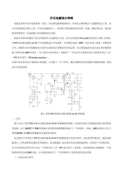
图1 采用FPS的基本反激式隔离AC-DC转换器一、引言图1示出了采用FPS的基本反激式隔离AC-DC转换器的原理图,它同时也是本文所描述的设计程序的参考电路。
由于MOSFET和PWM控制器以及各附加电路都被集成在了一个封装中,因此,SMPS的设计比分立型的MOSFET和PWM控制器解决方案要容易得多。
本文提供了针对基于FPS的反激式隔离AC-DC转换器的进步式设计程序,也包括变压器设计、输出滤波器设计、元件选择和反馈闭合环路设计。
这里描述的设计程序具有足够的通用性,可适用于不同的应用。
本文介绍的设计程序还可以由一个软件设计工具(FPS设计助手)来实现,从而使得设计师能够在一个很短的时间内完成SMPS设计。
本文的附录给出了一个采用软件工具的步进式设计实例。
二、步进式设计程序在这一节中,我们以图1所示的原理为参考来介绍设计程序。
一般而言,如图1所示,大多数FPS 引脚1到引脚4的配置都是相同的。
(1)第一步:确定系统规格输入电压范围(V line min 和V line max )。

高效率开关电源设计实例以下设计实例中,包括了各种技巧来提高开关电源的总体效率。
有源钳位和元损吸收电路的设计主要依托阅历来完成的,所以不在这里引见。
采用新技术时必需小心,由于很多是有专利的,能够需求直接付专利费给专利持有人,或在购置每一片控制IC芯片时,支付附加费用。
在将这些电源引入消费前,请留意这个效果。
10W同步整流Buck变换器运用此设计实例是PWM设计实例1的再设计,它包括了如何设计同步整流器(板载的10W降压Buck变换器)。
在设计同步整流开关电源时,必需细心选择控制IC。
为了效率最高和体积最小,普通同步控制器在系统功用上各有所长,使得控制器只是在供应商提到的运用场所中功用较好。
很多运转功用的巧妙之处不能确定,除非仔细读过数据手册。
例如,每当作者试图设计一个同步整流变换器,并试图运用现成买来的IC芯片时,3/4设计会被丢弃。
这是由于买来的芯片功用或任务形式往往无法改动。
更不用说,当发现现成方案不能满足需求时,是令人懊丧的(见图20的电路图)。
设计目的输入电压范围: DC+10~+14V输入电压: DC+5.0V额外输入电流: 2.0A过电流限制: 3.0A输入纹波电压: +30mV(峰峰值)输入调整:±1%最大任务温度: +40℃〝黑箱〞预估值输入功率: +5.0V*2A=10.0W(最大)输入功率: Pout/估量效率=10.0W/0.90=11.1W功率开关损耗 (11.1W-10W) * 0.5=0.5W续流二极管损耗: (1l.lW-10W)*0.5=0.5W输入平均电流低输入电压时 11.1W/10V=1.1lA高输入电压时: 11.1W/14V=0.8A估量峰值电流: 1.4Iout(rated)=1.4×2.0A=2.8A设计任务频率为300kHz。
电感设计(参见正激式滤波扼流圈的设计)最恶劣的任务状况是在高输入电压时。
式中Vin(max)——能够的最大输入电压。


江苏科技大学本科毕业设计(论文)学院电气与信息工程学院专业电子信息工程学生姓名李和琦班级学号0945531122指导教师丁伟二零一三年六月江苏科技大学本科毕业论文18W高效率反激开关电源的设计Design of 18W Efficient Flyback Switching Power Supply摘要任何电子设备都离不开可靠的电源,而对于采用电网电源的家用电子设备,其直流电源必须具有适应电网电压变化和负载变化的特性。
为此而发展的的直流稳压电源成为电子设备电路中的一个非常重要的组成部分。
开关电源是利用现代电力电子技术,以高频变压器代替工频变压器,采用脉宽调制技术的交流-直流的稳压电源,它具有管耗小,效率高,稳压范围宽及体积小,重量轻等特点,并广泛应用于工业自动化控制,军工设备,科研设备,LED照明,工控设备,通讯设备,电力设备,仪器设备,医疗设备,半导体制冷等领域。
本文主要内容如下:1.了解开关电源的基本结构,阅读开关电源相关文献,确定毕业设计所要做的内容;2.对开关电源的基本工作原理进行分析,对电源的buck工作模式,boost工作模式,buck-boost工作模式以及flybuck工作模式进行分析比较,最终选择适用于反激开关电源的flybuck工作模式;3.查阅资料学习了设计开关电源的基本方法,以及在设计过程中所需要掌握的原理,设计出一款输出功率为18W,输出电压与电流分别为12V,1.5A,文波小于150mV的高效率反激式开关电源;4.对设计出的实物进行波形分析。
测试其在工作过程中buck电容的电压电流变化,RCD回路上的电压吸收情况,MOS管在高压和断续时的Vds和Vgs电压,空载时的Vcc和Vds电压以及Sense电阻上的电压,对实物的基本特性进行测试。
关键词:直流稳压电源,开关电源,脉宽调制,反激式,高效率AbstractAny electronic devi ce can’t do without reliable power, As for the use of grid power home electronics equipment, The DC power supply must have to adapt to changes in grid voltage and load characteristics. To this end the development of the DC power supply circuit in electronic devices become a very important part.Switching power supply is the use of modern power electronics,High frequency transformers instead of frequency transformers, Using pulse width modulation DC - DC power supply,It has consumed a small tube, high efficiency, wide voltage range and small size, light weight, And is widely used in industrial automation, military equipment, scientific equipment, LED lighting, industrial control equipment, communications equipment, electrical equipment, apparatus equipment, medical equipment, semiconductor refrigeration and other fields.The graduation design process, mainly for the following:1. Understand the basic structure of the switch power supply, switch power supply related literature, to determine the content of the graduation design to do;2. Analyze the basic working principle of switch power supply, the power of the buck mode, boost the work mode, buck - boost work models and flybuck work carries on the analysis comparison, the final choice is suitable for the flyback switching power supply of flybuck working mode;3. To learn the basic methods of design of switch power supply, and the need to master the principle in the design process, and designed A power output of 18 w, output voltage and current respectively for 12 V, 1.5 A, less than 150 mV Wen Bo the flyback type switch power supply with high efficiency;4. The waveform analysis was carried out on the design of physical objects. Test the buck in the working process of the capacitor voltage current changes, RCD circuit voltage absorption.Keywords:Dc regulated power supply, Switching power supply, Pulse width modulation, the flyback type, High efficiency目录第一章绪论 (1)1.1 研究背景与发展状况 (1)1.2 开关电源相关介绍 (2)1.3 本章小结 (3)第二章开关电源的工作原理介绍 (4)2.1 基本拓扑结构 (4)2.1.1 Buck降压变换器 (4)2.1.2 Boost升压变换器 (6)2.1.3 Buck-Boost降压或升压变换器 (7)2.2 Flyback模式 (9)2.2.1 Buck-Boost拓扑Flyback (9)2.2.2 工作原理 (9)2.2.3 主要关系推导 (12)2.3本章小结 (13)第三章开关电源基本结构及元器件介绍 (14)3.1 开关电源基本结构 (14)3.2 开关电源主要器件 (15)3.2.1 TL431 (15)3.2.2 通嘉LD7531 (16)3.2.3 光耦 (16)3.2.4 安规电容 (17)3.3 本章小结 (17)第四章反激式开关电源的参数计算 (18)4.1课题介绍 (18)4.2 原理图和一般工作过程 (18)4.3 确定DC电压范围和输入整流滤波电容 (19)4.3.1 确定DC电压范围 (19)4.3.2 确定整流滤波电容 (20)4.4 反激式变压器的设计 (20)4.5 确定次级整流二极管 (24)4.6 确定输出电容 (24)4.7 RCD缓冲器的参数设计 (24)4.8 反馈回路的参数设计 (27)4.9 Sense电阻大小的确定 (28)4.10 安规电容的参数确定 (28)4.11提高效率的方法 (29)4.12 本章小结 (30)第五章反激式开关电源的产品测试 (31)5.1 基本测试 (31)5.2 波形分析 (31)5.3 本章小结 (36)结论 (37)致谢 (38)参考文献 (39)第一章绪论1.1 研究背景与发展状况电源按工作状态一般可分为线性电源,开关电源。

开关电源PCB设计实例印制电路板的制作所有开关电源设计的最后一步就是印制电路板(PCB)的线路设计。
如果这部分设计不当,PCB也会使电源工作不稳定,发射出过量的电磁干扰(EMI)。
设计者的作用就是在理解电路工作过程的基础上,保证PCB设计合理。
开关电源中,有些信号包含丰富的高频分量,因而任何一条PCB引线都可能成为天线。
引线的长和宽影响它的电阻和电感量,进而关系到它们的频率响应。
即使是传送直流信号的引线,也会从邻近的引线上引入RF(射频)信号,使电路发生故障,或者把这干扰信号再次辐射出去。
所有传送交流信号的引线要尽可能短且宽。
这意味着任何与多条功率线相连的功率器件要尽可能紧挨在一起,以减短连线长度。
引线的长度直接与它的电感量和电阻量成比例,它的宽度则与电感量和电阻量成反比。
引线长度就决定了其响应信号的波长,引线越长,它能接收和传送的干扰信号频率就越低,它所接收到的RF(射频)能量也越大。
主要电流环路每一个开关电源内部都有四个电流环路,每个环路要与其他环路分开。
由于它们对PCB布局的重要性,下面把它们列出来:1.功率开关管交流电流环路。
2.输出整流器交流电流环路。
3.输入电源电流环路。
4.输出负载电流环路。
图1 a、b、c画出了三种主要开关电源拓扑的环路。
通常输入电源和负载电流环路并没有什么问题。
这两个环路上主要是在直流电流上叠加了一些小的交流电流分量。
它们一般有专门的滤波器来阻止交流噪声进入周围的电路。
输入和输出电流环路连接的位置只能是相应的输入输出电容的接线端。
输入环路通过近似直流的电流对输入电容充电,但它无法提供开关电源所需的脉冲电流。
输入电容主要是起到高频能量存储器的作用。
类似地,输出滤波电容存储来自输出整流器的高频能量,使输出负载环能以直流方式汲取能量。
因此,输入和输出滤波电容接线端的放置很重要。
如果输入或输出环与功率开关或整流环的连接没有直接接到电容的两端,交流能量就会从输入或输出滤波电容上流进流出,并通过输入和输出电流环“逃逸”到外面环境中。
Power IntegrationsDesign Example ReportTitle10W Compact Power Supply using TOP245RSpecification Input: 90 – 300 VAC Output: 6V / 1.67A Application Water PurifierAuthor Power Integrations Applications Department Document Number DER-107 Date October 26, 2005 Revision1.0Summary and Features• 66kHz operation to reduce switching losses in TOPSwitch-GX , reduce standbypower consumption and reduce burden on input EMI Filter • Low profile EFD20 ESHEILD transformer construction • Simple input π-filter • No Y-cap No X-cap• 450 VDC input capacitors for increased reliability for continuous 300 V RMSoperation• No heat sink design - D 2PAK TOPSwitch-GX and D-PAK output rectifier • 10 W (continuous) / 18 W (peak) in 1.6 X 2.5 X 1”The products and applications illustrated herein (including circuits external to the products and transformer construction) may be covered by one or more U.S. and foreign patents or potentially by pending U.S. and foreign patent applications assigned to Power Integrations. A complete list of Power Integrations’ patents may be found at .Table Of Contents1Introduction (3)2Power Supply Specification (4)3Schematic (5)4Circuit Description (6)4.1Input EMI Filtering (6)4.2TOPSwitch Primary (6)4.3Output Rectification (6)4.4Output Feedback (6)5PCB Layout (7)6Bill Of Materials (8)7Transformer Specification (9)7.1Electrical Diagram (9)7.2Electrical Specifications (9)7.3Materials (9)7.4Transformer Build Diagram (10)7.5Transformer Construction (10)8PIXL Transformer Spreadsheet (11)9Performance Data (15)9.1Efficiency (15)9.2No-load Input Power (15)9.3Regulation (16)9.3.1Load (16)9.3.2Line (16)10Waveforms (17)10.1Drain Voltage and Current, Normal Operation (17)10.2Output Voltage Start-up Profile at Full Load (17)10.3Drain Voltage and Current Start-up Profile (18)10.4Load Transient Response (Load Step) (19)10.5Output Ripple Measurements (20)10.5.1Ripple Measurement Technique (20)10.5.2Measurement Results (21)11Control Loop Measurements (22)11.1120 VAC Maximum and 3A Load (22)11.2240 VAC Maximum and 3A Load (23)12Conducted EMI (24)13Revision History (25)Important Notes:Although this board is designed to satisfy safety isolation requirements, the engineering prototype has not been agency approved. Therefore, all testing should be performed using an isolated source to provide power to the prototype board.Design Reports contain a power supply design specification, schematic, bill of materials, and transformer documentation. Performance data and typical operation characteristics are included. Typically only a single prototype has been built.1 IntroductionThis document is an engineering report describing a universal input 6 V / 10 W power supply utilizing a TOP245R. This power supply is intended to be used in a compact adapter for a water purification application. This supply has been design to operate at 300 VAC input continuously as well as provide a peak output current of 3 A for two minutes.The document contains the power supply specification, schematic, bill-of-materials, transformer documentation, printed circuit layout, and performance data.TopBottomFigure 1 – Populated Circuit Board Photograph2 Power Supply SpecificationDescriptionSymbolMinTypMaxUnitsCommentInputVoltageV IN 90 300 VAC 2 Wire – no P.E.Frequencyf LINE 47 50/60 64 HzNo-load Input Power (240 VAC) 0.5 WOutputOutput Voltage 1V OUT1 6 V± 5% Output Ripple Voltage 1V RIPPLE1 100 mV 20 MHz bandwidthOutput Current 1I OUT1 1.67 ATotal Output PowerContinuous Output PowerP OUT 10 WPeak Output PowerP OUT_PEAK 18 W 2 minute durationEfficiency η 75 % Measured at P OUT (10 W), 25o C EnvironmentalConducted EMIMeets CISPR22B / EN55022BSafety Designed to meet IEC950, UL1950Class IISurge 4 kV 1.2/50 µs surge, IEC 1000-4-5,Series Impedance:Differential Mode: 2 ΩCommon Mode: 12 ΩSurge 4 kV100 kHz ring wave, 500 A short circuit current, differential and common modeAmbient Temperature T AMB 0 40 oCFree convection, sea level3 SchematicFigure 2 – Schematic4 Circuit DescriptionThe schematic in Figure 2 shows an off-line Flyback converter using the TOP245R. The circuit is designed for 90 VAC to 300 VAC input and 6 V, 1.67 A output, with a transient load requirement of 3 A for 2 minutes in duration.4.1 Input EMI FilteringCapacitor C1, C2 and L1 form in input p-filter for differential-mode conducted EMI. Common-mode conducted EMI is reduced with the ESHIELD winding technique employed in the transformer construction. A input X-capacitor and a Y-capacitor to bridge the isolation barrier are not required, due to the ESHIELD transformer construction and frequency dithering of the TOPSwitch-GX.4.2 TOPSwitch PrimaryRectifier bridge BR1 and C1, C2 provide a high voltage DC BUS for the primary circuitry. The DC rail is applied to the primary winding of T2. The other side of the transformer primary is driven by the integrated MOSFET in U1. Diode D4, R7, R3 and C6 clamp leakage spikes generated when the MOSFET in U1 switches off. Resistor R8 sets the low-line turn-on threshold to approximately 69 VAC, and also sets the over-voltage shutdown level to approximately 320 VAC. R2 sets the U1 current limit to approximately 75% of its nominal value. This limits the output power delivered during fault conditions. C5 bypasses the U1 CONTROL pin. C4 has 3 functions. It provides the energy required by U1 during startup, sets the auto-restart frequency during fault conditions, and also acts to roll off the gain of U1 as a function of frequency. R1 adds a zero to stabilize the power supply control loop. Diode D3 and C12 provide rectified and filtered bias power for U3 and U1. The Frequency pin (F-pin) of U1 is tied to the Control pin (C-pin) to set the operating frequency of the U1 to 66kHz.4.3 Output RectificationThe output of T2 is rectified and filtered by D6, C9, and C10. Inductor L2 and C11 provide additional high frequency filtering.4.4 Output FeedbackResistors R9 and R10 divide down the supply output voltage and apply it to the reference pin of error amplifier U2. Shunt regulator U2 drives optocoupler U3 through resistor R12 to provide feedback information to the U1 CONTROL pin. The optocoupler output also provides power to U1 during normal operating conditions.Components C4, C13, R1, R11, and R12 all play a role in compensating the power supply control loop. Capacitor C4 rolls off the gain of U1 at relatively low frequency. Resistor R1 provides a zero to cancel the phase shift of C4. Resistor R12 sets the gain of the direct signal path from the supply output through U2 and U3. Components C13 and R11 roll off the gain of U2.5 PCB LayoutFigure 3 – Printed Circuit Layout6 Bill Of Materials7 Transformer Specification7.1 Electrical DiagramFigure 4 – Transformer Electrical Diagram7.2 Electrical SpecificationsElectrical Strength 1 second, 60 Hz, from Pins 1-4 to Pins 5-8 3000VACPrimary Inductance Pins 3-4, all other windings open, measured at100 kHz, 0.4 VRMS 606 µH, -7/+7%Resonant Frequency Pins 3-4, all other windings open 800 kHz (Min.)Primary Leakage Inductance Pins 3-4, with Pins 5-8 shorted, measured at100kHz, 0.4 VRMS100 µH (Max.)7.3 MaterialsItem Description[1] Core: EFD20/3F3 AL = 104nH/T2[2] Bobbin: 8-pin[3] Magnet Wire: #35 AWG Heavy Build[4] Magnet Wire: #27 AWG Heavy Build[5] Tape: 3M 3mm wide[6] Tape, 3M[7] Tape, 3M[8] Copper tape 1.5 mil thick X 8mm wide[9] Varnish7.4 Transformer Build DiagramFigure 5 – Transformer Build Diagram 7.5 Transformer ConstructionBobbin Preparation Align bobbin to have pins 1-4 facing the mandrillPrimary Margin Apply 3 mm wide margin on either side of bobbin with item [5]. Match height of primary and bias windings.Primary Start at Pin 3. Wind 76 turns of item [3] in approximately 2 layers, finish on Pin 4.Basic Insulation Use one layer of item [6] for basic insulation.Bias Winding Starting at Pin 2, wind 14 turns of item [3] uniformly across bobbin width in a single layer. Finish at Pin 1.Basic Insulation Use one layer of item [6] for basic insulation.Primary Margin Apply 3 mm wide margin on either side of bobbin with item [5]. Match height of balanced shield winding.Balanced Shield Winding Start temporarily on pin 6. Wind 4 turns of quadrifilar item [4] uniformly across the bobbin width in a single layer. Finish on pin 4. Cut start of winding at 90-degree bend to center of bobbin window.ReinforcedInsulationUse three layers of item [7] for reinforced insulation.Secondary Margin Apply 3 mm wide margin on either side of bobbin with item [5]. Match height of secondary winding.Secondary Winding Start at Pin 5. Wind 6 trifilar turns of item [4]. Spread turns evenly across bobbin in a single layer. Finish on Pin 8.Outer Wrap Wrap windings with 3 layers of tape (item [7]). Core Preparation Affix cores (item [1]) with tape [5].Outer Belly band Wrap one turn of copper tape [8] around outer core. Ensure copper tape makes contact with core halves. Solder wire from pin 2 of bobbin to copper bellyband.Final Assembly Wrap three layers of tape [7]. Varnish impregnate (item [9]).8 PIXL Transformer SpreadsheetACDC_TOPSwitchGX_113004;Rev.2.2; Copyright PowerIntegrations Inc. 2004 INPUT INFO OUTPUT UNIT TOP_GX_FX_113004.xls:TOPSwitch-GX/FXContinuous/DiscontinuousFlyback Transformer DesignSpreadsheetENTER APPLICATION VARIABLESVACMIN 85 VoltsVACMAX 300 Volts Maximum AC Input VoltagefL 50 Hertz AC Mains FrequencyVO 6 Volts Output VoltagePO 18 Watts Output Powern 0.73 Efficiency EstimateZ 0.5 Loss Allocation FactorVB 15 Volts Bias VoltagetC 3 mSeconds Bridge Rectifier Conduction TimeEstimateCIN 44 uFarads Input Filter CapacitorENTER TOPSWITCH-GX VARIABLESTOP-GX TOP245 Universal 115 Doubled/230VChosen Device TOP245 PowerOut60W 85WKI 0.8 External Ilimit reduction factor(KI=1.0 for default ILIMIT, KI<1.0 for lower ILIMIT) ILIMITMIN 1.296 Amps Use 1% resistor in settingexternal ILIMITILIMITMAX 1.584 Amps Use 1% resistor in settingexternal ILIMITFrequency (F)=132kHz, (H)=66kHz h Half (H) frequency option -66kHzfS 66000 Hertz TOPSwitch-GX SwitchingFrequency: Choose between132 kHz and 66 kHzfSmin 61500 Hertz TOPSwitch-GX MinimumSwitching FrequencyfSmax 70500 Hertz TOPSwitch-GX MaximumSwitching FrequencyVOR 82 Volts Reflected Output VoltageVDS 10 Volts TOPSwitch on-state Drain toSource VoltageVD 0.5 Volts Output Winding Diode ForwardVoltage DropVDB 0.7 Volts Bias Winding Diode ForwardVoltage DropKP 0.9415 Ripple to Peak Current Ratio(0.4 < KRP < 1.0 : 1.0<KDP<6.0)ENTER TRANSFORMER CORE/CONSTRUCTION VARIABLESCore Type efd20Core EFD20 P/N: EFD20-3F3Bobbin EFD20_BOBBIN P/N: CSH-EFD20-1S-8PAE 0.58 0.58 cm^2 Core Effective Cross SectionalAreaLE 5.7 5.7 cm Core Effective Path LengthAL 1800 1800 nH/T^2 Ungapped Core EffectiveInductanceBW 16.4 16.4 mm Bobbin Physical Winding Width M 3 mm Safety Margin Width (Half thePrimary to Secondary CreepageDistance)L 2 Number of Primary LayersNS 6 Number of Secondary Turns DC INPUT VOLTAGE PARAMETERSVMIN 81 Volts Minimum DC Input Voltage VMAX 424 Volts Maximum DC Input Voltage CURRENT WAVEFORM SHAPE PARAMETERSDMAX 0.54 Maximum Duty CycleIAVG 0.30 Amps Average Primary CurrentIP 1.07 Amps Peak Primary CurrentIR 1.01 Amps Primary Ripple CurrentIRMS 0.47 Amps Primary RMS Current TRANSFORMER PRIMARY DESIGN PARAMETERSLP 606 uHenries Primary InductanceNP 76 Primary Winding Number ofTurnsNB 14 Bias Winding Number of Turns ALG 106 nH/T^2 Gapped Core EffectiveInductanceBM 1480 Gauss Maximum Flux Density at PO,VMIN (BM<3000)BP 2187 Gauss Peak Flux Density (BP<4200) BAC 696 Gauss AC Flux Density for Core LossCurves (0.5 X Peak to Peak)ur 1408 Relative Permeability ofUngapped CoreLG 0.65 mm Gap Length (Lg > 0.1 mm) BWE 20.8 mm Effective Bobbin WidthOD 0.27 mm Maximum Primary WireDiameter including insulation INS 0.05 mm Estimated Total InsulationThickness (= 2 * film thickness) DIA 0.22 mm Bare conductor diameterAWG 32 AWG Primary Wire Gauge (Roundedto next smaller standard AWGvalue)CM 64 Cmils Bare conductor effective area incircular milsCMA Warning 137 Cmils/Amp !!!!!!!!!! INCREASE CMA>200(increase L(primary layers),decreaseNS, larger Core) TRANSFORMER SECONDARY DESIGN PARAMETERS (SINGLE OUTPUT EQUIVALENT)Lumped parametersISP 13.52 Amps Peak Secondary CurrentISRMS 5.48 Amps Secondary RMS CurrentIO 3.00 Amps Power Supply Output Current IRIPPLE 4.59 Amps Output Capacitor RMS RippleCurrentCMS 1097 Cmils Secondary Bare Conductorminimum circular milsAWGS 19 AWG Secondary Wire Gauge(Rounded up to next largerstandard AWG value)DIAS 0.91 mm Secondary Minimum BareConductor DiameterODS 1.73 mm Secondary Maximum OutsideDiameter for Triple InsulatedWireINSS 0.41 mm Maximum Secondary InsulationWall ThicknessVOLTAGE STRESS PARAMETERSVDRAIN 616 Volts Maximum Drain VoltageEstimate (Includes Effect ofLeakage Inductance)PIVS 40 Volts Output Rectifier Maximum PeakInverse VoltagePIVB 96 Volts Bias Rectifier Maximum PeakInverse Voltage TRANSFORMER SECONDARY DESIGN PARAMETERS (MULTIPLE OUTPUTS)1st outputVO1 6.0 6 Volts Output VoltageIO1 3.000 3 Amps Output DC CurrentPO1 18.00 Watts Output PowerVD1 0.5 0.5 Volts Output Diode Forward VoltageDropNS1 6.00 Output Winding Number of Turns ISRMS1 5.484 Amps Output Winding RMS Current IRIPPLE1 4.59 Amps Output Capacitor RMS RippleCurrentPIVS1 40 Volts Output Rectifier Maximum PeakInverse VoltageCMS1 1097 Cmils Output Winding Bare Conductorminimum circular milsAWGS1 19 AWG Wire Gauge (Rounded up to nextlarger standard AWG value) DIAS1 0.91 mm Minimum Bare ConductorDiameterODS1 1.73 mm Maximum Outside Diameter forTriple Insulated Wire2nd outputVO2 6.0 Volts Output VoltageIO2 1.670 Amps Output DC CurrentPO2 10.02 Watts Output PowerVD2 0.5 Volts Output Diode Forward VoltageDropNS2 6.00 Output Winding Number of TurnsISRMS2 3.053 Amps Output Winding RMS Current IRIPPLE2 2.56 Amps Output Capacitor RMS RippleCurrentPIVS2 40 Volts Output Rectifier Maximum PeakInverse VoltageCMS2 611 Cmils Output Winding Bare Conductorminimum circular milsAWGS2 22 AWG Wire Gauge (Rounded up to nextlarger standard AWG value) DIAS2 0.65 mm Minimum Bare ConductorDiameterODS2 1.73 mm Maximum Outside Diameter forTriple Insulated Wire9 Performance DataAll measurements performed at room temperature, 60 Hz input frequency. 9.1 EfficiencyFigure 6 – Efficiency vs. Input Voltage, Room Temperature, 60 Hz.9.2 No-load Input PowerFigure 7 – Zero Load Input Power vs. Input Line Voltage, Room Temperature, 60 Hz9.3 Regulation 9.3.1 LoadFigure 8 – Load Regulation, Room Temperature9.3.2 LineFigure 9 – Line Regulation, Room Temperature, Full Load10 Waveforms10.1 Drain Voltage and Current, Normal OperationFigure 10 – 90 VAC, Full Load.Upper: I DRAIN , 0.5 A / divLower: V DRAIN , 100 V, 2 µs / divFigure 11– 265 VAC, Full LoadUpper: I DRAIN , 0.5 A / div Lower: V DRAIN , 200 V / div10.2 Output Voltage Start-up Profile at Full LoadFigure 12 – Start-up Profile, 120VAC1 V,2 ms / div.Figure 13 – Start-up Profile, 240 VAC1 V,2 ms / div.10.3 Drain Voltage and Current Start-up ProfileFigure 14 – 90 VAC Input and Maximum Load.Upper: I DRAIN, 0.5 A / div.Lower: V DRAIN, 100 V & 1 ms / div.Figure 15 – 265 VAC Input and Maximum Load.Upper: I DRAIN, 0.5 A / div.Lower: V DRAIN, 200 V & 1 ms / div.10.4 Load Transient Response (Load Step)In the figures shown below, signal averaging was used to better enable viewing the load transient response. The oscilloscope was triggered using the load current step as a trigger source. Since the output switching and line frequency occur essentially at random with respect to the load transient, contributions to the output ripple from these sources will average out, leaving the contribution only from the load step response.Figure 16 – Transient Response, 120VAC, 75-100-75% Load Step.Bottom: Load Current, 1 A/div.Top: Output Voltage2000 mV, 5V offset, 1ms / div.Figure 17 – Transient Response, 120VAC, 100-180-100% Load StepBottom: Load Current, 1 A/ div.Top: Output Voltage200 mV 5V offset, 1 ms / div.10.5 Output Ripple Measurements10.5.1 Ripple Measurement TechniqueFor DC output ripple measurements, a modified oscilloscope test probe must be utilized in order to reduce spurious signals due to pickup. Details of the probe modification are provided in Figure 18and Figure 19.The 5125BA probe adapter is affixed with two capacitors tied in parallel across the probetip. The capacitors include one (1) 0.1 µF/50 V ceramic type and one (1) 1.0µF/50 Valuminum electrolytic. The aluminum electrolytic type capacitor is polarized, so proper polarity across DC outputs must be maintained (see below).Figure 18 – Oscilloscope Probe Prepared for Ripple Measurement. (End Cap and Ground Lead Removed)Figure 19 – Oscilloscope Probe with Probe Master 5125BA BNC Adapter. (Modified with wires for probe ground for ripple measurement, and two parallel decoupling capacitors added)Probe Tip10.5.2 Measurement ResultsFigure 20 – Ripple, 120VAC, Full Load.2 ms, 20 mV / div Figure 21 – Ripple, 240VAC, Full Load.2 ms, 20 mV / div11 Control Loop Measurements11.1 120 VAC Maximum and 3A LoadFigure 22 – Gain-Phase Plot, 120 VAC, Maximum Steady State LoadVertical Scale: Gain = 8 dB/div, Phase = 40 °/div.Crossover Frequency = 2.66 kHz Phase Margin = 88.11°Figure 23 – Gain-Phase Plot, 120 VAC, 3A LoadVertical Scale: Gain = 12 dB/div, Phase = 40 °/div.Crossover Frequency = 1.32 kHz Phase Margin = 84.02°11.2240 VAC Maximum and 3A LoadFigure 24 – Gain-Phase Plot, 240 VAC, Maximum Steady State LoadVertical Scale: Gain = 8 dB/div, Phase = 40 °/div.Crossover Frequency = 11.11 kHz Phase Margin = 57.14°Figure 25 – Gain-Phase Plot, 240 VAC, 3A LoadVertical Scale: Gain = 12 dB/div, Phase = 40 °/div.Crossover Frequency = 7.26 kHz Phase Margin = 71.65°12 Conducted EMIFigure 26 – Maximum Steady State Load, 120 VAC/60 Hz, and EN55022 B Limits (LINE)Figure 27 –Maximum Steady State Load, 120VAC/60Hz, and EN55022 B Limits (Neutral)Figure 28 –Maximum Steady State Load, 240VAC/ 60 Hz, and EN55022 B Limits (LINE)Figure 29 –Maximum Steady State Load, 240VAC/60Hz, and EN55022 B Limits (Neutral)13 Revision HistoryDate Author Revision Description & changes ReviewedRelease KM/JC/VC 10-26-05 RSP 1.0 InitialFor the latest updates, visit our website:Power Integrations reserves the right to make changes to its products at any time to improve reliability or manufacturability. Power Integrations does not assume any liability arising from the use of any device or circuit described herein. POWER INTEGRATIONS MAKES NO WARRANTY HEREIN AND SPECIFICALLY DISCLAIMS ALL WARRANTIES INCLUDING, WITHOUT LIMITATION, THE IMPLIED WARRANTIES OF MERCHANTABILITY, FITNESS FOR A PARTICULAR PURPOSE, AND NON-INFRINGEMENT OF THIRD PARTY RIGHTS.PATENT INFORMATIONThe products and applications illustrated herein (including transformer construction and circuits external to the products) may be covered by one or more U.S. and foreign patents, or potentially by pending U.S. and foreign patent applications assigned to Power Integrations.A complete list of Power Integrations’ patents may be found at . Power Integrations grants its customers a license under certain patent rights as set forth at /ip.htm.The PI Logo, TOPSwitch, TinySwitch,LinkSwitch,DPA-Switch,EcoSmart, PI Expert and PI FACTS are trademarks of Power Integrations, Inc. Other trademarks are property of their respective companies. ©Copyright 2005 Power Integrations, Inc.Power Integrations Worldwide Sales Support LocationsWORLD HEADQUARTERS 5245 Hellyer AvenueSan Jose, CA 95138, USA. Main: +1-408-414-9200 Customer Service:Phone: +1-408-414-9665 Fax: +1-408-414-9765e-mail: usasales@ GERMANYRueckertstrasse 3D-80336, MunichGermanyPhone: +49-89-5527-3910Fax: +49-89-5527-3920e-mail: eurosales@JAPANKeihin Tatemono 1st Bldg2-12-20Shin-Yokohama, Kohoku-ku,Yokohama-shi, Kanagawa ken,Japan 222-0033Phone: +81-45-471-1021Fax: +81-45-471-3717e-mail:japansales@TAIWAN5F, No. 318, Nei Hu Rd., Sec. 1Nei Hu Dist.Taipei, Taiwan 114, R.O.C.Phone: +886-2-2659-4570Fax: +886-2-2659-4550e-mail:taiwansales@CHINA (SHANGHAI)Rm 807-808A,Pacheer Commercial Centre, 555 Nanjing Rd. West Shanghai, P.R.C. 200041 Phone: +86-21-6215-5548 Fax: +86-21-6215-2468e-mail: chinasales@ INDIA261/A, Ground Floor7th Main, 17th Cross,SadashivanagarBangalore, India 560080Phone: +91-80-5113-8020Fax: +91-80-5113-8023e-mail: indiasales@KOREARM 602, 6FLKorea City Air Terminal B/D,159-6Samsung-Dong, Kangnam-Gu,Seoul, 135-728, KoreaPhone: +82-2-2016-6610Fax: +82-2-2016-6630e-mail:koreasales@EUROPE HQ1st Floor, St. James’s HouseEast Street, FarnhamSurrey, GU9 7TJUnited KingdomPhone: +44 (0) 1252-730-140Fax: +44 (0) 1252-727-689e-mail: eurosales@CHINA (SHENZHEN)Room 2206-2207, Block A, Elec. Sci. Tech. Bldg.2070 Shennan Zhong Rd. Shenzhen, Guangdong, China, 518031Phone: +86-755-8379-3243 Fax: +86-755-8379-5828 e-mail: chinasales@ ITALYVia Vittorio Veneto 1220091 Bresso MIItalyPhone: +39-028-928-6000Fax: +39-028-928-6009e-mail: eurosales@SINGAPORE51 Newton Road,#15-08/10 Goldhill Plaza,Singapore, 308900Phone: +65-6358-2160Fax: +65-6358-2015e-mail:singaporesales@APPLICATIONS HOTLINEWorld Wide +1-408-414-9660APPLICATIONS FAXWorld Wide +1-408-414-9760。