NE664M04中文资料
- 格式:pdf
- 大小:131.68 KB
- 文档页数:9
目录一:E60,M64的联接 (2)1:E60-NC联接 (2)2:基本I/O联接 (4)3:M64S-NC (6)4:伺服系统的联接 (8)5:E60,M60系列系统联接总图 (9)二:外围线路的检查及上电注意事项 (12)三:参数的设定 (12)1:基本参数的设定 (12)2:轴参数的设定 (14)3:原点复归参数 (14)4:伺服参数的设定 (15)5:主轴参数的设定 (17)6:机械误差 (18)7:PLC (18)8:巨程式,位置开关详见操作手册 (19)四.PLC程序的输入 (19)1:PLC4B格式PLC传输 (19)2:GPPW格式PLC程序输入 (20)3:PLC系统部分运行测试 (21)五:资料备份及恢复 (22)1:RS-232C传输方式 (22)2:资料备份卡存储方式 (23)六:附录 (24)1:伺服参数标准设定表(未列明的系列请参照手册) (24)2:主轴参数(未列明的请参照手册) (25)3:SVJ2伺服参数的优化 (28)4:模具加工经验参数及高速高精度的使用 (29)5:三菱相关软件 (30)一:E60,M64的联接1:E60-NC 联接(1)E60-NC (FCU6-MU071)接口图:CRTLCDNCKBNCKB系统键盘的联接F053(2)控制单元联接系统图(3)*紧急停止按钮的配线:三菱E60及64系列以后的紧急停止的配线与以往系统的配线有本质区别,现在急停端口内部为有源输出,如果外部贸然接入电源,有可能造成短路而烧毁NC。
望用户引起注意。
例:2:基本I/O联接(1)HR341/HR351端口图:CF31/CF32/CF33/CF34插头DI:CF31/CF32注1:漏/源改变联接,请给COM提供以下电压漏:DC24V源:0V注2:I/O口的电源与基本I/O的DCIN回路不同,请单独加载直流电源。
DO:CF33/CF34注1:±10V模拟电压输出,与基本I/O单元AO端口功能相同。
雷蒙m6600说明书
由于缺少详细说明书,以下是一些有关Dell Precision M6600的通用信息:
Dell Precision M6600是一款高性能移动工作站,适用于专业设计师、工程师、科学家和其他需要高端计算机运算能力与可靠性的用户。
规格:
- 处理器:Intel Core i5/i7或Xeon E3/E4系列
- 显卡:Nvidia Quadro 5000M
- 内存:最大支持32GB DDR3
- 存储:最大支持3个硬盘,其中1个可选的mSATA SSD
- 显示器:17.3英寸LED背光屏幕,分辨率可达1920x1080 - 光驱:DVD刻录机或Blu-ray刻录机
- 网络:Gigabit以太网、无线802.11n Wi-Fi、蓝牙4.0、可选4G LTE无线连接
- 输入输出端口:USB 3.0、eSATA、DisplayPort、HDMI、VGA、音频输出和输入、SD卡读卡器等
- 操作系统:Windows 7或Windows 10
其他特点包括:
- 铝制机身和强化碳纤维材料,经过军事标准测试,可承受恶劣环境下的使用和运输
- 支持高清视频会议,包括HD摄像头和双向音频
- 支持指纹识别、智能卡和TPM安全芯片,确保数据的保密性和完整性
- 支持快速启动技术和自动备份,以保证数据的安全
- 支持外接扩展坞和多屏幕显示
总之,Dell Precision M6600是一款专业级别的高性能移动工作站,具有强大的计算能力、可靠的性能和坚固的设计。

品牌:国内知名品牌服务器外型:机架式服务器高度:2UCPU类型:Intel Xeon 六核/八核E5-2600 v4系列处理器CPU实配规格:1颗8核E5-2620V4 2.1GHzCPU可扩展数量:≥2颗智能技术:要求支持智能处理器导槽安装技术,避免人为安装故障芯片组:Intel C610以上内存类型:DDR4-2133MHz内存实配规格:32GB内存可扩展数量:≥512GB,≥16个内存插槽内存保护技术:Advanced ECC,Online Spare内存保护技术内存验证技术:要求支持内存智能验证技术,能够智能验证内存及支持原厂内存增强功能内置硬盘类型:2.5寸或3.5寸热插拔SAS硬盘内置硬盘实配规格:3块1T SATA 3.5 7.2K内置硬盘可扩展数量:最大16个SFF硬盘或12个LFF硬盘阵列控制器:标配12Gb SAS磁盘阵列控制器, ≥2GB FBWC缓存,支持RAID 0/1/5/6/60/ADM高级数据镜像/;最大可支持到4GB FBWC 缓存且服务器故障断电情况下阵列卡缓存数据保护不受时间限制,可额外增加智能电池,为同一机箱内所有的智能阵列卡提供断电数据保护功能,且使用寿命不低于7年网卡:标配板载双端口千兆以太网卡,可选扩展卡扩展四端口Flex-LOM 模块化以太网卡,可选升级为2个10Gb或10Gb base-T 网络模块或Infiniband 存储模块电源:1个550W高效电源智能安装引导:服务器集成智能导航, 支持引导安装操作系统, 硬件检测, RAID配置,部件驱动程序等,无需额外光盘支持远程管理卡:可选/标配独立的远程管理控制端口,可选/标配高级管理功能;能独立于操作系统实现对服务器的远程控制及管理;虚拟电源开关,远程开/关机;远程Firmware升级功能;128bit加密支持;VPN连接;虚拟介质功能,支持软驱、光驱、ISO文件、文件目录的虚拟;虚拟字符及图形远程控制台;多用户共享访问被管理服务器;捕获及重放被管理服务器的运行界面;被管理服务器的环境温度及能耗的监控和分析,动态监控服务器功率及供电情况,智能优化调整供电功率并节省能源消耗管理软件:自我品牌管理软件,可实现管理自我品牌以及其他厂家品牌的小型机、存储、服务器、PC等在内的设备;实现硬件设备通过颜色、电子邮件方式报警、资产登记管理、服务器性能管理、软件补丁管理、自动化系统部署管理、电源功耗管理、虚拟机管理等功能;系统监控系统:监控系统可实时监测内部主要部件的状态,包含CPU、内存、PCI槽、风扇、电源、温度等信息启动特性:可支持UEFI BIOS或传统BIOS启动虚拟存储:标配VSA虚拟存储软件,1TB标准授权,可将服务器虚拟为专业存储设备售后服务:三年现场,7*24,当天4小时到场免费惠普金牌服务故障前预报警服务:提供处理器,内存,硬盘故障前预警,故障前问题时予以免费保修文档:完整文档、电源线等包装:原厂完整包装。
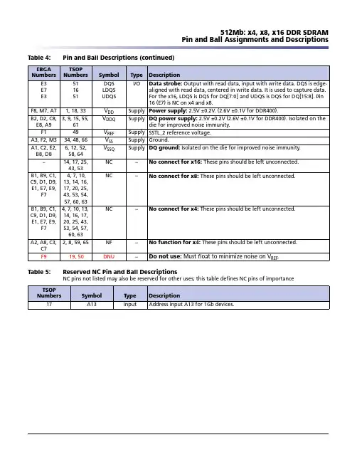
512Mb: x4, x8, x16 DDR SDRAM Pin and Ball Assignments and Descriptions E3E7E3511651DQS LDQS UDQS I/O Data strobe: Output with read data, input with write data. DQS is edge-aligned with read data, centered in write data. It is used to capture data. For the x16, LDQS is DQS for DQ[7:0] and UDQS is DQS for DQ[15:8]. Pin16 (E7) is NC on x4 and x8.F8, M7, A71, 18, 33V DD Supply Power supply: 2.5V ±0.2V. (2.6V ±0.1V for DDR400).B2, D2, C8, E8, A93, 9, 15, 55, 61V DDQ Supply DQ power supply: 2.5V ±0.2V (2.6V ±0.1V for DDR400). Isolated on the die for improved noise immunity.F149V REF Supply SSTL_2 reference voltage.A3, F2, M334, 48, 66V SS Supply Ground.A1, C2, E2, B8, D86, 12, 52, 58, 64V SSQ Supply DQ ground: Isolated on the die for improved noise immunity.–14, 17, 25, 43, 53NC –No connect for x16: These pins should be left unconnected.B1, B9, C1, C9, D1, D9, E1, E7, E9, F7 4, 7, 10,13, 14, 16,17, 20, 25,43, 53, 54,57, 60, 63NC –No connect for x8: These pins should be left unconnected.B1, B9, C1, C9, D1, D9, E1, E7, E9, F74, 7, 10, 13,14, 16, 17,20, 25, 43,53, 54, 57,60, 63NC –No connect for x4: These pins should be left unconnected.A2, A8, C3, C72, 8, 59, 65NF –No function for x4: These pins should be left unconnected.F9 19, 50DNU –Do not use: Must float to minimize noise on V REF .Table 5:Reserved NC Pin and Ball Descriptions NC pins not listed may also be reserved for other uses; this table defines NC pins of importance TSOP NumbersSymbol Type Description 17A13Input Address input A13 for 1Gb devices.Table 4:Pin and Ball Descriptions (continued)FBGA NumbersTSOP Numbers Symbol Type Description512Mb: x4, x8, x16 DDR SDRAMElectrical Specifications – I DDTable 7: I DD Specifications and Conditions (x16) Die Revision F OnlyV DDQ = 2.6V ±0.1V, V DD = 2.6V ±0.1V (-5B); V DDQ = 2.5V ±0.2V, V DD = 2.5V ±0.2V (-6, -6T, -75E, -75Z, -75);0°C d T A d 70°C; Notes: 1–5, 11, 13, 15, 47; Notes appear on pages 37–42; See also Table 10 on page 20Parameter/Condition Symbol-5B-6/6T-75E-75Z/-75Units NotesI DD0155130130115mA23, 48 Operating one-bank active-precharge current:t RC = t RC (MIN); t CK = t CK (MIN); DQ, DM, and DQS inputschanging once per clock cycle; Address and control inputschanging once every two clock cyclesI DD1195160160145mA23, 48 Operating one-bank active-read-precharge current:Burst = 4; t RC = t RC (MIN); t CK = t CK (MIN); I OUT = 0mA;Address and control inputs changing once per clock cycleI DD2P5555mA24, 33 Precharge power-down standby current: All banks idle;Power-down mode; t CK = t CK (MIN); CKE = (LOW)I DD2F55454540mA51 Idle standby current: CS# = HIGH; All banks are idle;t CK = t CK (MIN); CKE = HIGH; Address and other controlinputs changing once per clock cycle; V IN = V REF for DQ, DQS,and DMI DD3P45353530mA24, 33 Active power-down standby current: One bank active;Power-down mode; t CK = t CK (MIN); CKE = LOWI DD3N60505045mA23 Active standby current: CS# = HIGH; CKE = HIGH; One bankactive;t RC = t RAS (MAX); t CK = t CK (MIN); DQ, DM, and DQSinputs changing twice per clock cycle; Address and othercontrol inputs changing once per clock cycleI DD4R210165165145mA23, 48 Operating burst read current: Burst = 2; Continuousburst reads; One bank active; Address and control inputschanging once per clock cycle; t CK = t CK (MIN); I OUT = 0mAI DD4W215195160135mA23 Operating burst write current: Burst = 2; Continuous burstwrites;One bank active; Address and control inputs changingonce per clock cycle; t CK = t CK (MIN); DQ, DM, and DQS inputschanging twice per clock cycleAuto refresh burst current:t RFC = t RFC (MIN)I DD5345290290280mA50t RFC = 7.8µs IDD5A11101010mA28, 50t RFC = 1.95µs IDD5A16151515mA28, 50 Self refresh current: CKE d 0.2V Standard I DD66555mA12Low power (L)I DD6A4333mA12I DD7480405400350mA23, 49 Operating bank interleave read current: Four bankinterleaving READs (burst = 4) with auto precharge,t RC = minimum t RC allowed; t CK = t CK (MIN); Address andcontrol inputs change only during active READ or WRITEcommands。
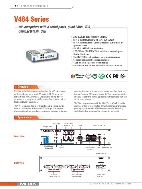
The V464 embedded computers are based on the AMD x86 processor, and feature 4 serial ports, quad LAN ports, 4 USB 2.0 hosts, and CompactFlash. A VGA interface is also included, making the V464 computers particularly well-suited for industrial applications such as SCADA and factory automation.The V464 computers’ 4 serial ports can be used to connect a wide range of serial devices, and the quad 10/100 Mbps Ethernet ports offer a reliable solution for network redundancy, promising continuousFront Viewoperation for data communication and management. In addition, the CompactFlash and USB sockets provide the V464 computers with the reliability needed for industrial applications that require data buffering and storage expansion.The V464 computers come with the WinCE 6.0 or WinXP Embedded operating system already installed. WinCE 6.0 and WinXP Embedded provide programmers with a friendly environment for developingsophisticated, bug-free application software at a lower cost.OverviewAppearanceRear View10/100 Mbps SocketSerial Ports x 2Serial Ports x 2 9-36 VDCComputerCPU:******************************************,500 MHzOS (pre-installed): Windows CE 6.0 or Windows XP Embedded System Chipset: AMD CS5536BIOS: 4 Mbit Flash BIOS, supporting Plug & Play, APM 1.2, ACPI 1.0 SRAM: 256 KB, battery backupFSB: 400 MHzSystem Memory: 200-pin SO-DIMM socket with built-in 256 MB (CE) or 512 MB (XPe) DDR, supporting DDR400 up to 1 GB Expansion Bus: PC/104-Plus onboardUSB: USB 2.0 compliant hosts x 4, type A connector, supports system boot upStorageBuilt-in: 256 MB (CE) or 1 GB (XPe) industrial DOM for OS Storage Expansion: CompactFlash socketOther PeripheralsKB/MS: 1 PS/2 interface supporting standard PS/2 keyboard and mouse through Y-type cableAudio: AC97 audio, with line-out interfaceDisplayGraphics Controller: CPU integrated 2D graphicsDisplay Interface: CRT interface for VGA outputEthernet InterfaceLAN: 4 10/100 Mbps, auto-sensing (RJ45) portsController: Realtek RTL8100CLMagnetic Isolation Protection: 1.5 KV built-inSerial InterfaceSerial Standards:• 2 RS-232 ports (DB9 male)• 2 RS-232/422/485 ports, software selectable (DB9 male)ESD Protection: 15 KV for all signalsSerial Communication ParametersData Bits: 5, 6, 7, 8Stop Bits: 1, 1.5, 2Parity: None, Even, Odd, Space, MarkFlow Control: RTS/CTS, XON/XOFF, ADDC® (automatic data direction control) for RS-485Baudrate: 50 bps to 921.6 Kbps (non-standard baudrates supported; see user’s manual for details)Serial SignalsRS-232: TxD, RxD, DTR, DSR, RTS, CTS, DCD, GNDRS-422: TxD+, TxD-, RxD+, RxD-, GND RS-485-4w: TxD+, TxD-, RxD+, RxD-, GNDRS-485-2w: Data+, Data-, GNDLEDsSystem: Power, Battery, StorageLAN: 10M/Link x 2, 100M/Link x 2 (on connector)Switches and ButtonsPower Switch: on/offReset Button: For warm rebootPhysical CharacteristicsHousing: AluminumWeight: 1.32 kgDimensions:Without ears: 223 x 121 x 57 mm (8.78 x 4.76 x 2.24 in)With ears: 248 x 140 x 70 mm (9.76 x 5.51 x 2.76 in)Mounting: DIN-Rail, wallEnvironmental LimitsOperating Temperature: -10 to 60°C (14 to 140°F)Operating Humidity: 5 to 95% RHStorage Temperature: -20 to 80°C (-4 to 176°F)Anti-vibration: 5 g rms @ IEC-68-2-34, random wave, 5-500 Hz, 1 hr per axisAnti-shock: 50 g @ IEC-68-2-27, half sine wave, 11 msPower RequirementsInput Voltage: 9 to 36 VDC (3-pin terminal block for V+, V-, SG) Power Consumption: 26 W• 730 mA @ 36 VDC• 1080 mA @ 24 VDC• 2820 mA @ 9 VDCRegulatory ApprovalsEMC: CE (EN55022 Class A, EN61000-3-2 Class A, EN61000-3-3, EN55024), FCC (Part 15 Subpart B, CISPR 22 Class A), CCC (GB9254, GB 17625.1)Safety: UL/cUL (UL60950-1, CSA C22.2 No. 60950-1-03), LVD, CCC (GB4943)Green Product: RoHS, cRoHS, WEEEReliabilityAlert Tools: Built-in buzzer and RTC (real-time clock) with battery backupAutomatic Reboot Trigger: Built-in WDT (watchdog timer) supporting 1-255 level time interval system reset, software programmable WarrantyWarranty Period: 3 yearsDetails: See /warrantyHardware SpecificationsWindows Embedded CE 6.0System Utilities: Windows command shell, telnet, ftpFile System: FAT (on-board flash)Protocol Stack: TCP, UDP, IPv4, SNMP V2, ICMP, IGMP, ARP, HTTP, CHAP, PAP, SSL, DHCP, SNTP, SMTP, Telnet, FTP, PPP Telnet Server: Allows remote administration through a standard telnet client.FTP Server: Used for transferring files to and from remote computer systems over a network.File Server: Enables clients to access files and other resources over the network (Microsoft® Wincows® CE).Web Server (httpd): Includes ASP, ISAPI Secure Socket Layer support, SSL 2, SSL 3, and Transport Layer Security (TLS/SSL 3.1) public key-based protocols, and Web Administration ISAPI Extensions.Dial-up Networking Service: RAS client API and PPP, supporting Extensible Authentication Protocol (EAP) and RAS scripting. Watchdog Service: CPU Hardware function to reset CPU in a user specified time interval (triggered by calling a MOXA library function).Application Development Software:• Moxa WinCE 6.0 SDK• C Libraries and Run-times• Component Services (COM and DCOM)• Microsoft® .NET Compact Framework 2.0 SP2• XML, including DOM, XQL, XPATH, XSLT, SAX, SAX2• SOAP Toolkit Client• Winsock 2.2Software SpecificationsWindows XP EmbeddedSystem Utilities: Windows command shell, Telnet, ftp, Wireless Zero Configuration File System: NTFSProtocol Stack: DHCP, IPv4, DNS, IPsec, HTTP, TCP, UDP, ICMP, IGMP, ARP, TAPI, TSP, SNMP V2, NTP, ICS, PPP, CHAP, EAP, SNTP, Telnet, SNTP, FTP, SMTP, PPPoE, PPTP, NetBIOSTelnet Server: Allows users to connect to Telnet servers from remote computers.IIS Web Server: Allows you to create and manage Web sites.Terminal Server: Microsoft Terminal Server client application (mstsc.exe).COM+ Services: The next evolution of Microsoft Component Object Model (COM) and Microsoft Transaction Server (MTS).Computer Browser Service: Computer browsing functionalityexposed by Windows through Microsoft Networking. Allows a client machine to browse its network neighborhood for available computers exposing file and print sharing services.Disk Management Services: Support for disk and volumemanagement operations. The component implements a Component Object Model (COM) interface that can be used to query and configure disks and volumes, both basic and dynamic. The component also monitors disk arrivals and removals and other changes in the storage subsystem.Remote Registry Service: Enables remote users to modify registry settings on this computer.Application Development Software:• Microsoft .Net Framework 2.0 with service pack 2 (CLR and the .NET Framework class library)• Active Directory Service Interface (ADSI) Core • Active Template Library (ATL), 2.0• Certificate Request Client & Certificate Autoenrollment (CLR and the .NET Framework class library) • COM APIs• Common Control Libraries • Common File Dialogs• Direct3D, DirectPlay, DirectShow and Direct show filters • Distributed Transaction Coordinator (MSDTC)• Enhanced Write Filter (Redirect disk write operations to volatile (RAM) or non-volatile (disk) storage) • Event Log, Internet Explorer • Mapi32 Libraries• Message Queuing (MSMQ) Core• Microsoft Visual C++ Run Time Libraries • Power Management dynamic-link library • Registry Editor • RPC• Smart Card Cryptographic Service Providers• USB 2.0 core drivers compliant with The USB .95 or 1.0 • Windows API, Media Player 10, Script Engines, and WMIV464 computer• Ethernet cable: RJ45 to RJ45 cross-over • cable, 100 cmDIN-rail Mounting Kit• PS2 to KB/MS Y-type Cable• Document and Software CD or DVD • Quick Installation Guide (printed)• Product Warranty Statement (printed)• Package ChecklistAvailable ModelsV464-CE: x86 embedded computer with 4 serial ports, quad LANs, VGA, CompactFlash, USB, and WinCE 6.0 OSV464-XPE: x86 embedded computer with 4 serial ports, quad LANs, VGA, CompactFlash, USB, and Windows XP Embedded OSOptional Accessories (can be purchased separately)PWR-24250-DT-S1: Power adaptorPWC-C7US-2B-183: Power cord with 2-pin connector, USA plug PWC-C7EU-2B-183: Power cord with 2-pin connector, Euro plug PWC-C7UK-2B-183: Power cord with 2-pin connector, British plug PWC-C7AU-2B-183: Power cord with 2-pin connector, Australia plug PWC-C7CN-2B-183: Power cord with 2-pin connector, China plugOrdering Information。
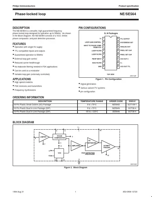
FUNCTIONAL DESCRIPTION(Figure 6)The NE564 is a monolithic phase-locked loop with a post detection processor. The use of Schottky clamped transistors and optimized device geometries extends the frequency of operation to greater than 50MHz.In addition to the classical PLL applications, the NE564 can be used as a modulator with a controllable frequency deviation.The output of the PLL can be written as shown in the following equation:V O =(f IN - f O)K VCO(1)K VCO = conversion gain of the VCOf IN = frequency of the input signalf O = free-running frequency of the VCOThe process of recovering FSK signals involves the conversion of the PLL output into logic compatible signals. For high data rates, a considerable amount of carrier will be present at the output of the PLL due to the wideband nature of the loop filter. To avoid the use of complicated filters, a comparator with hysteresis or Schmitt trigger is required. With the conversion gain of the VCO fixed, the output voltage as given by Equation 1 varies according to the frequency deviation of f IN from f O. Since this differs from system to system, it is necessary that the hysteresis of the Schmitt trigger be capable of being changed, so that it can be optimized for a particular system. This is accomplished in the 564 by varying the voltage at Pin 15 which results in a change of the hysteresis of the Schmitt trigger. For FSK signals, an important factor to be considered is the drift in the free-running frequency of the VCO itself. If this changes due to temperature, according to Equation 1 it will lead to a change in the DC levels of the PLL output, and consequently to errors in the digital output signal. This is especially true for narrowband signals where the deviation in f IN itself may be less than the change in f O due to temperature. This effect can be eliminated if the DC or average value of the signal is retrieved and used as the reference to the comparator. In this manner, variations in the DC levels of the PLL output do not affect the FSK output.VCO SectionDue to its inherent high-frequency performance, an emitter-coupled oscillator is used in the VCO. In the circuit, shown in the equivalent schematic, transistors Q21 and Q23 with current sources Q25 - Q26 form the basic oscillator. The approximate free-running frequency of the oscillator is shown in the following equation:f O≅122 R C (C1 + C S)(2)R C = R19 = R20 = 100Ω (INTERNAL)C1 = external frequency setting capacitorC S = stray capacitanceVariation of V D (phase detector output voltage) changes the frequency of the oscillator. As indicated by Equation 2, the frequency of the oscillator has a negative temperature coefficient due to the monolithic resistor. To compensate for this, a current I R with negative temperature coefficient is introduced to achieve a low frequency drift with temperature.Phase Comparator SectionThe phase detection processor consists of a doubled-balanced modulator with a limiter amplifier to improve AM rejection.Schottky-clamped vertical PNPs are used to obtain TTL level inputs. The loop gain can be varied by changing the current in Q4 and Q15 which effectively changes the gain of the differential amplifiers. This can be accomplished by introducing a current at Pin 2.Post Detection Processor SectionThe post detection processor consists of a unity gain transconductance amplifier and comparator. The amplifier can be used as a DC retriever for demodulation of FSK signals, and as a post detection filter for linear FM demodulation. The comparator has adjustable hysteresis so that phase jitter in the output signal can be eliminated.As shown in the equivalent schematic, the DC retriever is formed by the transconductance amplifier Q42 - Q43 together with an external capacitor which is connected at the amplifier output (Pin 14). This forms an integrator whose output voltage is shown in the following equation:V O =g MC2(3)V IN dtg M = transconductance of the amplifierC2 = capacitor at the output (Pin 14)V IN = signal voltage at amplifier inputWith proper selection of C2, the integrator time constant can be varied so that the output voltage is the DC or average value of the input signal for use in FSK, or as a post detection filter in linear demodulation.The comparator with hysteresis is made up of Q49 - Q50 with positive feedback being provided by Q47 - Q48. The hysteresis is varied by changing the current in Q52 with a resulting variation in the loop gain of the comparator. This method of hysteresis control, which is a DC control, provides symmetric variation around the nominal value.Design FormulaThe free-running frequency of the VCO is shown by the following equation:(4)f O≅122 R C (C1 + C S)R C = 100ΩC1 = external cap in faradsC S = stray capacitanceThe loop filter diagram shown is explained by the following equation:(5)f S =11 + sRC3(First Order)R = R12 = R13 = 1.3kΩ (Internal)*By adding capacitors to Pins 4 and 5, a pole is added to the loop transfer atω =1RC3NOTE:*Refer to Figure 6.SR01035Figure 11. Phase Comparator (Pins 4 and 5) and FSK (Pin 16) OutputsBIAS ADJUST+5VCER.INPUT SIGNALNE564DET.VCO OUTPUTLOOP FILTERVCO67381213911541012.47µF CER..47µF .33µF.33µF f = Nxf T C O.47µFf TNxf T*510Ω1k Ω2kI 210k÷N510Ω*NOTE:Use R 9-11 only if rise time is critical.Figure 12. NE564 Phase-Locked Frequency Multiplier。
fresh mode, the DLL remains disabled even upon exit of SELF REFRESH operation untilit is re-enabled and reset.The DRAM is not tested to check—nor does Micron warrant compliance with—normalmode timings or functionality when the DLL is disabled. An attempt has been made tohave the DRAM operate in the normal mode where reasonably possible when the DLLhas been disabled; however, by industry standard, a few known exceptions are defined:•ODT is not allowed to be used•The output data is no longer edge-aligned to the clock•CL and CWL can only be six clocksWhen the DLL is disabled, timing and functionality can vary from the normal operationspecifications when the DLL is enabled (see DLL Disable Mode (page 125)). Disablingthe DLL also implies the need to change the clock frequency (see Input Clock Frequen-cy Change (page 129)).Output Drive StrengthThe DDR3 SDRAM uses a programmable impedance output buffer. The drive strengthmode register setting is defined by MR1[5, 1]. RZQ/7 (34ȍ [NOM]) is the primary outputdriver impedance setting for DDR3 SDRAM devices. To calibrate the output driver im-pedance, an external precision resistor (RZQ) is connected between the ZQ ball andV SSQ. The value of the resistor must be 240ȍ ±1%.The output impedance is set during initialization. Additional impedance calibration up-dates do not affect device operation, and all data sheet timings and current specifica-tions are met during an update.To meet the 34ȍ specification, the output drive strength must be set to 34ȍ during initi-alization. To obtain a calibrated output driver impedance after power-up, the DDR3SDRAM needs a calibration command that is part of the initialization and reset proce-dure.OUTPUT ENABLE/DISABLEThe OUTPUT ENABLE function is defined by MR1[12], as shown in Figure 56 (page146). When enabled (MR1[12] = 0), all outputs (DQ, DQS, DQS#) function when in thenormal mode of operation. When disabled (MR1[12] = 1), all DDR3 SDRAM outputs(DQ and DQS, DQS#) are tri-stated. The output disable feature is intended to be usedduring I DD characterization of the READ current and during t DQSS margining (writeleveling) only.TDQS EnableTermination data strobe (TDQS) is a feature of the x8 DDR3 SDRAM configuration thatprovides termination resistance (R TT) and may be useful in some system configurations.TDQS is not supported in x4 or x16 configurations. When enabled via the mode register(MR1[11]), the R TT that is applied to DQS and DQS# is also applied to TDQS and TDQS#.In contrast to the RDQS function of DDR2 SDRAM, DDR3’s TDQS provides the termina-tion resistance R TT only. The OUTPUT DATA STROBE function of RDQS is not providedby TDQS; thus, R ON does not apply to TDQS and TDQS#. The TDQS and DM functionsshare the same ball. When the TDQS function is enabled via the mode register, the DMfunction is not supported. When the TDQS function is disabled, the DM function is pro-vided, and the TDQS# ball is not used. The TDQS function is available in the x8 DDR3DLL Disable ModeIf the DLL is disabled by the mode register (MR1[0] can be switched during initializationor later), the DRAM is targeted, but not guaranteed, to operate similarly to the normalmode, with a few notable exceptions:•The DRAM supports only one value of CAS latency (CL = 6) and one value of CASWRITE latency (CWL = 6).•DLL disable mode affects the read data clock-to-data strobe relationship (t DQSCK),but not the read data-to-data strobe relationship (t DQSQ, t QH). Special attention isrequired to line up the read data with the controller time domain when the DLL is dis-abled.•In normal operation (DLL on), t DQSCK starts from the rising clock edge AL + CLcycles after the READ command. In DLL disable mode, t DQSCK starts AL + CL - 1 cy-cles after the READ command. Additionally, with the DLL disabled, the value oft DQSCK could be larger than t CK.The ODT feature (including dynamic ODT) is not supported during DLL disable mode.The ODT resistors must be disabled by continuously registering the ODT ball LOW byprogramming R TT,nom MR1[9, 6, 2] and R TT(WR) MR2[10, 9] to 0 while in the DLL disablemode.Specific steps must be followed to switch between the DLL enable and DLL disablemodes due to a gap in the allowed clock rates between the two modes (t CK [AVG] MAXand t CK [DLL_DIS] MIN, respectively). The only time the clock is allowed to cross thisclock rate gap is during self refresh mode. Thus, the required procedure for switchingfrom the DLL enable mode to the DLL disable mode is to change frequency during selfrefresh:1.Starting from the idle state (all banks are precharged, all timings are fulfilled, ODTis turned off, and R TT,nom and R TT(WR) are High-Z), set MR1[0] to 1 to disable theDLL.2.Enter self refresh mode after t MOD has been satisfied.3.After t CKSRE is satisfied, change the frequency to the desired clock rate.4.Self refresh may be exited when the clock is stable with the new frequency fort CKSRX. After t XS is satisfied, update the mode registers with appropriate values.5.The DRAM will be ready for its next command in the DLL disable mode after thegreater of t MRD or t MOD has been satisfied. A ZQCL command should be issuedwith appropriate timings met.。
DDR2 SDRAM SODIMMMT16HTF12864HZ – 1GB MT16HTF25664HZ – 2GBMT16HTF51264HZ – 4GB Features•200-pin, small-outline dual in-line memory module (SODIMM)•Fast data transfer rates: PC2-3200, PC2-4200,PC2-5300, or PC2-6400•1GB (128 Meg x 64), 2GB (256 Meg x 64) or 4GB (512Meg x 64)•V DD = V DDQ = 1.8V •V DDSPD = 1.7–3.6V•JEDEC-standard 1.8V I/O (SSTL_18-compatible)•Differential data strobe (DQS, DQS#) option •4n -bit prefetch architecture•Multiple internal device banks for concurrent operation•Programmable CAS latency (CL)•Posted CAS additive latency (AL)•WRITE latency = READ latency - 1 t CK •Programmable burst lengths (BL): 4 or 8•Adjustable data-output drive strength •64ms, 8192-cycle refresh •On-die termination (ODT)•Halogen-free•Serial presence detect (SPD) with EEPROM •Gold edge contacts •Dual rankFigure 1: 200-Pin SODIMM (MO-224 R/C E)OptionsMarking•Operating temperature–Commercial (0°C ≤ T A ≤ +70°C)None –Industrial (–40°C ≤ T A ≤ +85°C)1I •Package–200-pin DIMM (halogen-free)Z •Frequency/CL 2– 1.87ns @ CL = 7 (DDR2-1066)-1GA – 2.5ns @ CL = 5 (DDR2-800)-80E – 2.5ns @ CL = 6 (DDR2-800)-800–3ns @ CL = 5 (DDR2-667)-667Notes:1.Contact Micron for industrial temperaturemodule offerings.2.CL = CAS (READ) latency.3.Not recommended for new designs.Table 1: Key Timing ParametersTable 2: AddressingTable 3: Part Numbers and Timing Parameters – 1GB Modules1Table 4: Part Numbers and Timing Parameters – 2GB Modules1Table 5: Part Numbers and Timing Parameters – 2GB Modules1Notes:1.The data sheet for the base device can be found on Micron’s Web site.2.All part numbers end with a two-place code (not shown) that designates component and PCB revisions.Consult factory for current revision codes. Example: MT16HTF25664HZ-80EM1.1GB, 2GB, 4GB (x64, DR) 200-Pin DDR2 SDRAM SODIMMFeatures质量等级领域:宇航级IC、特军级IC、超军级IC、普军级IC、禁运IC、工业级IC,军级二三极管,功率管等;应用领域:航空航天、船舶、汽车电子、军用计算机、铁路、医疗电子、通信网络、电力工业以及大型工业设备祝您:工作顺利,生活愉快!以深圳市美光存储技术有限公司提供的参数为例,以下为MT46H64M16LFBF-5IT_B的详细参数,仅供参考Electrical SpecificationsStresses greater than those listed may cause permanent damage to the module. This is a stress rating only, and functional operation of the module at these or any other condi-tions outside those indicated in the device data sheet are not implied. Exposure to abso-lute maximum rating conditions for extended periods may adversely affect reliability.1GB, 2GB, 4GB (x64, DR) 200-Pin DDR2 SDRAM SODIMMElectrical Specifications。
ArchitecturePipeline RegistersThe output from the multiplier can feed a pipeline register or this registercan be bypassed. Pipeline registers may be implemented for anymultiplier size and increase the DSP block’s maximum performance,especially when using the subsequent DSP block adder stages. Pipelineregisters split up the long signal path between theadder/subtractor/accumulator block and the adder/output block,creating two shorter paths.Adder/Output BlockThe adder/output block has the following elements:■An adder/subtractor/accumulator block■ A summation block■An output select multiplexer■Output registersFigure6–7 shows the adder/output block architecture.The adder/output block can be configured as:■An output interface■An accumulator which can be optionally loaded■ A one-level adder■ A two-level adder with dynamic addition/subtraction control on thefirst-level adder■The final stage of a 36-bit multiplier, 9 × 9 complex multiplier, or18×18 complex multiplierThe output select multiplexer sets the output configuration of the DSPblock. The output registers can be used to register the output of theadder/output block.1The adder/output block cannot be used independently from themultiplier.Fast Passive Parallel ConfigurationFPP Configuration Using a MicroprocessorIn the FPP configuration scheme, a microprocessor can control thetransfer of configuration data from a storage device, such as flashmemory, to the target Stratix II or Stratix II GX device.1All information in “FPP Configuration Using a MAX II Deviceas an External Host” on page7–15 is also applicable when usinga microprocessor as an external host. Refer to that section for allconfiguration and timing information.FPP Configuration Using an Enhanced Configuration DeviceIn the FPP configuration scheme, an enhanced configuration device sendsa byte of configuration data every DCLK cycle to the Stratix II orStratix II GX device. Configuration data is stored in the configurationdevice.1When configuring your Stratix II or Stratix II GX device usingFPP mode and an enhanced configuration device, the enhancedconfiguration device decompression feature is available whilethe Stratix II and Stratix II GX decompression and designsecurity features are not.Figure7–8 shows the configuration interface connections between aStratix II or Stratix II GX device and the enhanced configuration devicefor single device configuration.1The figures in this chapter only show the configuration-relatedpins and the configuration pin connections between theconfiguration device and the device.f For more information on the enhanced configuration device and flashinterface pins, such as PGM[2..0], EXCLK, PORSEL, A[20..0], andDQ[15..0], refer to the Enhanced Configuration Devices (EPC4, EPC8 &EPC16) Data Sheet in volume 2 of the Configuration Handbook.DC & Switching CharacteristicsThe maximum clock toggle rate is different from the maximum data bitrate. If the maximum clock toggle rate on a regular I/O pin is 300MHz,the maximum data bit rate for dual data rate (DDR) could be potentiallyas high as 600 Mbps on the same I/O pin.Table5–77 specifies the maximum input clock toggle rates. Table5–78specifies the maximum output clock toggle rates at 0pF load. Table5–79specifies the derating factors for the output clock toggle rate for a non 0pFload.To calculate the output toggle rate for a non 0pF load, use this formula:The toggle rate for a non 0pF load= 1000 / (1000/ toggle rate at 0pF load + derating factor * load valuein pF /1000)For example, the output toggle rate at 0pF load for SSTL-18 Class II 20mAI/O standard is 550MHz on a -3 device clock output pin. The deratingfactor is 94ps/pF. For a 10pF load the toggle rate is calculated as:1000 / (1000/550 + 94 × 10 /1000) = 363 (MHz)Tables5–77 through 5–79 show the I/O toggle rates for Stratix IIdevices.Table5–77.Maximum Input Toggle Rate on Stratix II Devices(Part 1 of2)Input I/O Standard Column I/O Pins (MHz)Row I/O Pins (MHz)Dedicated Clock Inputs(MHz)-3-4-5-3-4-5-3-4-5LVTTL500500450500500450500500400 2.5-V LVTTL/CMOS500500450500500450500500400 1.8-V LVTTL/CMOS500500450500500450500500400 1.5-V LVTTL/CMOS500500450500500450500500400 LVCMOS500500450500500450500500400 SSTL-2 Class I500500500500500500500500500 SSTL-2 Class II500500500500500500500500500 SSTL-18 Class I500500500500500500500500500 SSTL-18 Class II500500500500500500500500500 1.5-V HSTL Class I500500500500500500500500500 1.5-V HSTL Class II500500500500500500500500500 1.8-V HSTL Class I500500500500500500500500500。
浪潮英信服务器NF8460M4产品简介2016年10月本文档为售前工程师、对技术感兴趣的销售人员/客户提供一个浪潮服务器NF8460M4的简单规格介绍。
适合销售人员、售前工程师参考,以及服务器用户了解产品技术。
浪潮英信服务器NF8460M4灵动可靠稳定高效的四路4U机架式服务器⏹产品定位浪潮英信NF8460M4是一款采用英特尔至强™处理器E7-8800/4800 v3/v4 产品家族计算平台技术的中高端四路服务器,具备均衡的性能表现和良好的可靠性、可用性。
在系统设计、易用性、高能效比、扩展性和噪音优化方面都有全面的提升。
⏹目标用户适用于政府、教育、大中型企业等行业对系统能效比和稳定性有着较高要求的市场⏹产品特性均衡优异的性能表现●4路处理器,96颗计算核心,192个计算线程●最大支持32条内存,满足海量内存需求●可支持卡式PCIe SSD、2.5寸SATA SSD●高性能12G SAS RAID控制器支持1、2、4GB缓存●E7 v4/v3计算平台最佳性价比设计易于维护的系统架构●主要部件采用模块化易拆卸维护,提高系统维护效率●硬盘、电源、风扇冗余,支持热插拔●全系统温控,精准控制散热系统平稳安静运行持续优化的扩展能力●支持多代平台平滑升级,保护用户投资●最大支持24块2.5寸硬盘扩展,本地存储能力出众●12个PCIe插槽,支持全长全高,支持MIC或GPU协处理卡⏹应用举例●大中型数据库●虚拟化解决方案;●商业智能分析;●中间件应用;●高性能计算;⏹产品规格产品图片仅供参考,请以销售实物为准;详细的技术规格和供货情况,请向浪潮当地经销商查询,如有变化,恕不另行通知。
若您想获得更加详细的产品技术参数和价格请拨打800-860-6708。
WAIN08-06HK-004/0,004/2 组合型插芯电流负载能力电流负载能力所受的限制主要来自包含接插针的接插体可承受的最大温度测试和控制过程依据DIN EN 60512-5DIN EN 60 664DIN EN 61 984接插件针数按照DIN EN 61984的电气数据电力区-额定电流 -额定电压 -额定脉冲电压 -污染程度-当污染程度2时的参数信号区-额定电流 -额定电压 -额定脉冲电压 -污染程度-当污染程度2时的参数依据UL/CSA额定电压绝缘电阻材料工作温度范围阻燃等级(UL 94)可拔插次数规范认证技术参数规范/认证插芯插针4/0+PE,4/2+PE80A 830V 8kV 380A 1000V 8kV 216A 400V 6kV 316A 400/690V 6kV 2600/300V ≥1010Ω聚碳酸酯-40℃...+125℃V0≥500电力区 -材料-表面处理 -接触电阻 -螺钉连接 -mm 2 -AWG -拧紧力矩 -mm 2 -N.m -剥线长度信号区 -材料-表面处理 -接触电阻 -螺钉连接 -mm 2 -AWG -拧紧力矩 -剥线长度铜合金镀银≤0.3mΩ1.5-16mm 216-61.52.5 4 6 10 161.2 2 3 3 3 314mm 铜合金镀银≤1mΩ0.5-2.5mm 220-140.5Nm 7.5mm 08 16 24 32 40 48 56 64 72 80 88 96 104 112 120 128 2030405060708090 100 110 120 130导线截面:16mm 2导线截面:10mm 2环境温度[℃]工作电流[A ]WAIN08-07插芯公母型号HK-004/0-M HK-004/0-F订货号128 004 011 0001128 004 021 0001螺丝连接830/400V 80/16A 4/0,4/2+插芯HK-004/0,004/2 组合型插芯1)接插体之间最大距离21mm接插针排序外壳尺寸:匹配 16B 外壳,详情请参考第15-70~15-107页.HK-004/0HK-004/2插芯公母型号HK-004/2-M HK-004/2-F订货号128 006 011 0001128 006 021 0001螺丝连接M84.577.5M3x10421.2273427F84.577.5M3x1044.21.227.73427HK。
512Mb: x4, x8, x16 DDR SDRAM CommandsCommandsTables 30 and 31 provide a quick reference of available commands. Two additional Truth Tables—Table 32 on page 46 and Table 33 on page 47—provide current state/next stateinformation.Notes: 1.DESELECT and NOP are functionally interchangeable.2.BA[1:0] provide bank address and A[n :0] (128Mb: n = 11; 256Mb and 512Mb: n = 12; 1Gb: n= 13) provide row address.3.BA[1:0] provide bank address; A[i:0] provide column address, (where A i is the most signifi-cant column address bit for a given density and configuration, see Table 2 on page 2) A10HIGH enables the auto precharge feature (non persistent), and A10 LOW disables the autoprecharge feature.4.Applies only to READ bursts with auto precharge disabled; this command is undefined (andshould not be used) for READ bursts with auto precharge enabled and for WRITE bursts.5.A10 LOW: BA[1:0] determine which bank is precharged. A10 HIGH: all banks are prechargedand BA[1:0] are “Don’t Care.”6.This command is AUTO REFRESH if CKE is HIGH; SELF REFRESH if CKE is LOW.7.Internal refresh counter controls row addressing while in self refresh mode, all inputs andI/Os are “Don’t Care” except for CKE.8.BA[1:0] select either the mode register or the extended mode register (BA0 = 0, BA1=0select the mode register; BA0 = 1, BA1 = 0 select extended mode register; other combina-tions of BA[1:0] are reserved). A[n :0] provide the op-code to be written to the selectedmode register.Table 30: Truth Table 1 – CommandsCKE is HIGH for all commands shown except SELF REFRESH; All states and se q uences not shown are illegal or reserved FunctionCS#RAS#CAS#WE#Address Notes DESELECTH X X X X 1NO OPERATION (NOP)L H H H X 1ACTIVE (select bank and activate row)L L H H Bank/row 2READ (select bank and column and start READ burst)L H L H Bank/col 3WRITE (select bank and column and start WRITE burst)L H L L Bank/col 3BURST TERMINATEL H H L X 4PRECHARGE (deactivate row in bank or banks)L L H L Code 5AUTO REFRESH or SELF REFRESH(enter self refresh mode)L L L H X 6, 7LOAD MODE REGISTERL L L L Op-code 8Table 31: Truth Table 2 – DM OperationUsed to mask write data, provided coincident with the corresponding dataName (Function)DMDQ Write enable LValid Write inhibitH X512Mb: x4, x8, x16 DDR SDRAM Commands•Refreshing: Starts with registration of an AUTO REFRESH command and ends when t RFC is met. After t RFC is met, the DDR SDRAM will be in the all banks idle state.•Accessing mode register: Starts with registration of an LMR command and ends when t MRD has been met. After t MRD is met, the DDR SDRAM will be in the all banks idle state.•Precharging all: Starts with registration of a PRECHARGE ALL command and ends when t RP is met. After t RP is met, all banks will be in the idle state.6.All states and se q uences not shown are illegal or reserved.7.Not bank-specific; re q uires that all banks are idle, and bursts are not in progress.8.May or may not be bank-specific; if multiple banks are to be precharged, each must be in a valid state for precharging.9.Not bank-specific; BURST TERMINATE affects the most recent READ burst, regardless of bank.10.READs or WRITEs listed in the Command/Action column include READs or WRITEs with auto precharge enabled and READs or WRITEs with auto precharge disabled.11.Re q uires appropriate DM masking.12.A WRITE command may be applied after the completion of the READ burst; otherwise, a BURST TERMINATE must be used to end the READ burst prior to asserting a WRITE com-mand.Notes: 1.This table applies when CKE n-1 was HIGH and CKE n is HIGH (see Table 35 on page 49) andafter t XSNR has been met (if the previous state was self refresh).Table 33: Truth Table 4 – Current State Bank n – Command to Bank mNotes:1–6 apply to the entire table; Notes appear on page 47Current State CS#RAS#CAS#WE#Command/Action Notes Any HX X X DESELECT (NOP/continue previous operation)LH H H NO OPERATION (NOP/continue previous operation)Idle XX X X Any command otherwise allowed to bank m Row activating, active, or precharging LL H H ACTIVE (select and activate row)LH L H READ (select column and start READ burst)7LH L L WRITE (select column and start WRITE burst)7LL H L PRECHARGE Read (auto precharge disabled)LL H H ACTIVE (select and activate row)LH L H READ (select column and start new READ burst)7LH L L WRITE (select column and start WRITE burst)7,9LL H L PRECHARGE Write (auto precharge disabled)LL H H ACTIVE (select and activate row)LH L H READ (select column and start READ burst)7,8LH L L WRITE (select column and start new WRITE burst)7LL H L PRECHARGE Read (with auto-precharge)LL H H ACTIVE (select and activate row)LH L H READ (select column and start new READ burst)7LH L L WRITE (select column and start WRITE burst)7,9LL H L PRECHARGE Write (with auto-precharge)LL H H ACTIVE (select and activate row)LH L H READ (select column and start READ burst)7LH L L WRITE (select column and start new WRITE burst)7L L H L PRECHARGE。