HCPL0730中文资料
- 格式:pdf
- 大小:243.12 KB
- 文档页数:12
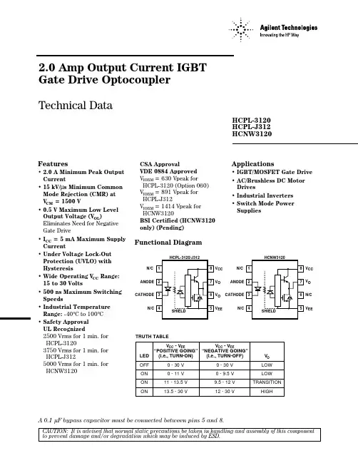
1-108HDual Channel Low Input Current, High Gain Optocouplers Technical DataFeatures• High Current Transfer Ratio – 1800% Typical • Low Input CurrentRequirements – 0.5 mA • Low Output Saturation Voltage – 0.1 V• High Density Packaging • Performance Guaranteed over Temperature 0°C to 70°C• LSTTL Compatible • High Output Current –60mA• Safety ApprovalUL Recognized - 2500 V rms for 1 Minute and5000V rms* for 1 minute CSA Approved• Available in 8 Pin DIP and SO-8 Footprint• MIL-STD-1772 VersionAvailable (HCPL-5730/5731)• Surface Mount Gull Wing Option Available for 8-Pin DIP (Option 300)Applications• Digital Logic Ground Isolation• Telephone Ring Detector • Level Shifting• EIA RS-232C Line Receiver • Polarity Sensing• Low Input Current LineReceiver - Long Line or Party Line• Microprocessor Bus Isolation• Current Loop Receiver• Line Voltage Status Indicator -Low Input Power DissipationHCPL-2730 HCPL-0730HCPL-2731 HCPL-0731DescriptionThese dual channel optocouplers contain a separated pair of GaAsP light emitting diodes optically coupled to a pair of integrated high gain photo detectors. They provide extremely high current transfer ratio and excellent input-output common mode transient immunity. A separate pin for the photodiodes and first gain stages (V CC ) permits lower output satura-tion voltage and higher speed operation than possible with conventional photodarlington type optocouplers. In addition,V CC may be as low as 1.6VFunctional DiagramCAUTION: It is advised that normal static precautions be taken in handling and assembly of this component to prevent damage and/or degradation which may be induced by ESD.*5000 V rms/1 minute withstand voltage rating is for Option 020 (HCPL-2730, HCLP-2731) products only.A 0.1 µF bypass capacitor connected between pins 5 and 8 is recommended.V O2V O1V CC GNDANODE 1CATHODE 1CATHODE 2ANODE 2TRUTH TABLE LED ON OFF V O LOW HIGH5965-3597Ewithout adversely affecting the parametric performance.These dual channel optocouplers are available in an 8-Pin DIP and in an industry standard SO-8 package. The following is a cross reference table listing the 8-Pin DIP part number and the electrically equivalent SOIC-8 part number.8-Pin DIP SO-8HCPL-2730HCPL-0730HCPL-2731HCPL-0731The SO-8 does not require “through holes” in a PCB. This package occupies approximately one-third the footprint area of the standard dual-in-line package. The lead profile is designed to be compatible with standard surface mount processes.Guaranteed operation at low inputcurrents and the high currenttransfer ratio (CTR) reduce themagnitude and effects of CTRdegradation.The outstanding high temperatureperformance of this splitDarlington type output amplifierresults from the inclusion of anintegrated emitter-base bypassresistor which shunts photodiodeand first stage leakage currents toground.The HCPL-2731/0731 have a400% minimum CTR at an inputcurrent of only 0.5 mA making itideal for use in low input currentapplications such as MOS, CMOS,and low power logic interfacing orRS232C data transmissionsystems. In addition, the highCTR and high output currentcapability make this deviceextremely useful in applicationswhere a high fanout is required.Compatibility with high voltageCMOS logic systems is guaranteedby the 18V V CC and V O specifica-tions and by testing output highleakage (I OH) at 18 V.The HCPL-2730/0730 are speci-fied at an input current of 1.6 mAand have a 7 V V CC and V O rating.The 300% minimum CTR allowsTTL to TTL interfacing at thisinput current.Important specifications such asCTR, leakage current, and outputsaturation voltage are guaranteedover the 0°C to 70°C temperaturerange to allow trouble-free systemoperation. Selection for lowerinput currents down to 250 µA isavailable upon request.Selection GuideWidebody8-Pin DIP Package Hermetic (300 Mil)Small Outline SO-8(400 mil)Single and Dual Single Dual Minimum Absolute Dual Single Channel Channel Channel Single Input ON Maxi-Channel Channel Package Package Package Channel Current Minimum mum Packages Package HCPL-HCPL-HCPL-Package(I F)CTR V CC HCPL-6N139[1]27310701[1]0731HCNW139[1]0.5 mA400%18 V6N138[1]27300700[1]0730HCNW138[1] 1.6 mA300% 7 VHCPL-4701[1]4731[1]070A[1]073A[1]40 µA800%18 V0.5 mA300%20 V5701[1]5700[1]5731[1]5730[1] Note:1. Technical data are on separate HP publications.1-1091-110Ordering InformationSpecify Part Number followed by Option Number (if desired).Example:HCPL-2731#XXX020 = 5000 V rms/1 Minute UL Rating Option.*300 = Gull Wing Surface Mount Option, 50 per tube.**500 = Tape and Reel Packaging Option, 1000 per reel.Option data sheets available. Contact your Hewlett-Packard sales representative or authorized distributor for information.*For HCPL-2731 and HCPL-2730 only.**Gull wing surface mount option applies to through hole parts only.SchematicGNDV O2V V CCV O1I V USE OF A 0.1 µF BYPASS CAPACITOR CONNECTEDBETWEEN PINS 5 AND 8 IS RECOMMENDED (SEE NOTE 8)DIMENSIONS IN MILLIMETERS AND (INCHES).0.254+ 0.076- 0.051(0.010+ 0.003)- 0.002)*MARKING CODE LETTER FOR OPTION NUMBERS"L" = OPTION 020OPTION NUMBERS 300 AND 500 NOT MARKED.Package Outline Drawings8-Pin DIP Package (HCPL-2731/HCPL-2730)8-Pin DIP Package with Gull Wing Surface Mount Option 300 (HCPL-2731/HCPL-2730)(0.025 ± 0.005)MAX.(0.100)BSCDIMENSIONS IN MILLIMETERS (INCHES).LEAD COPLANARITY = 0.10 mm (0.004 INCHES).+ 0.076- 0.051+ 0.003)- 0.002)1-1111-112Small Outline SO-8 Package (HCPL-0731/HCPL-0730)Note: Use of nonchlorine activated fluxes is highly recommended.Regulatory InformationThe HCPL-2731/2730 have been approved by the following organizations:ULRecognized under UL 1577,Component Recognition Program, File E55361.240TIME – MINUTEST E M P E R A T U R E – °C2202001801601401201008060402002600.228 ± 0.025 (0.012)MIN.DIMENSIONS IN MILLIMETERS (INCHES).LEAD COPLANARITY = 0.10 mm (0.004 INCHES).Solder Reflow Temperature Profile (HCPL-073X and Gull Wing Surface Mount Option 300 Parts).CSAApproved under CSA Component Acceptance Notice #5, File CA 88324.Insulation Related Specifications (HCPL-2731/2730/0731/0730)8-Pin DIP(300 Mil)SO-8Parameter Symbol Value Value Units ConditionsMinimum External Air L(101)7.1 4.9mm Measured from input terminals toGap (External output terminals, shortest distance Clearance)through air.Minimum External L(102)7.4 4.8mm Measured from input terminals to Tracking (External output terminals, shortest distance Creepage)path along body.Minimum Internal Plastic0.080.08mm Through insulation distance, conductor Gap (Internal Clearance)to conductor, usually the directdistance between the photoemitter andphotodetector inside the optocouplercavity.Tracking Resistance CTI200200Volts DIN IEC 112/ VDE 0303 Part 1 (Comparative TrackingIndex)Isolation Group IIIa IIIa Material Group DIN VDE 0110Option 300 – surface mount classification is Class A in accordance with CECC 00802.Absolute Maximum Ratings (No Derating Required up to 85°C)Parameter Symbol Min.Max.Units Storage Temperature T S-55125°C Operating Temperature T A-4085°C Average Forward Input Current I F(AVG)20mA Peak Forward Input Current I FPK40mA (50% Duty Cycle, 1 ms Pulse Width)Reverse Input Voltage (Each Channel)V R5V Input Power Dissipation (Each Channel)P I35mW Output Current (Each Channel)I O60mA Supply Voltage and Output Voltage V CC-0.518V (HCPL-2731, HCPL-0731)(V CC - Pin 8-5, V O - Pin 7,6-5) -Note 1Supply Voltage and Output Voltage V CC-0.57V (HCPL-2730, HCPL-0730)(V CC - Pin 8-5, V O - Pin 7,6-5) -Note 1Output Power Dissipation (Each Channel) -Note 12P O100mW Total Power Dissipation (Each Channel)P T135mW Lead Solder Temperature (for Through Hole Devices)260°C for 10 sec., 1.6 mm below seating plane Reflow Temperature Profile See Package Outline Drawings section(for SOIC-8 and Option #300)1-113Recommended Operating ConditionsParameter Symbol Min.Max.Units Power Supply Voltage (HCPL-2731/HCPL-0731)V CC 4.518V Power Supply Voltage (HCPL-2730/HCPL-0730)V CC 4.57V Forward Input Current (ON)I F(ON)0.512mA Forward Input Voltage (OFF)V F(OFF)00.8V Operating Temperature T A070°C1-1141-115Electrical Specifications0°C ≤T A ≤70°C, 4.5 V ≤V CC ≤18 V, 0.5 mA ≤I F(ON) ≤12 mA, 0 V ≤V F(OFF) ≤0.8 V, unless otherwise specified. All Typicals at T A = 25°C. (See note 8.)Device Parameter Sym.HCPL-Min.Typ.*Max.Units Test Conditions Fig.Note Current CTR273140018005000%I F = 0.5 mA V CC = 4.52, 32Transfer 0731V O = 0.4 V50016002600I F = 1.6 mA 2730/073030016002600I F = 1.6 mALogic Low V OL27310.10.4V I F = 1.6 mA, V CC = 4.5 V 1Output 0731I O = 8 mA Voltage0.10.4I F = 5.0 mA,I O = 15 mA 0.20.4I F = 12 mA,I O = 24 mA 2730/07300.10.4I F = 1.6 mA,I O = 4.8 mALogic High I OH2731/0731 0.05100µA V O = V CC = 18 V I F = 0 mA 2Output Current 2730/07310.1250V O = V CC = 7 VLogic Low I CCL 2731/07311.23mA V CC = 18 V I F1 = I F2 = 1.6 mA5Supply V 01 = V 02 = OpenCurrent 2730/07300.9V CC = 7 VLogic High I CCH 2731/07310.00520µAV CC = 18 V I F1 = I F2 = 0 mA,5Supply V 01 = V 02 = OpenCurrent 2730/0730 0.004V CC = 7 V Input V F1.41.7VT A = 25°C4Forward Voltage 1.75I F = 1.6 mAInput BV R5.0V I R = 10 µA, T A = 25°C2Reverse Breakdown Voltage Temperature ∆V F -1.8mV/°C I F = 1.6 mACoefficient ∆T Aof Forward Voltage InputC IN60pFf = 1 MHz, V F = 02Capacitance*All typical values at T A = 25°C and V CC = 5 V, unless otherwise noted.Ratio1-116DeviceParameter Sym.HCPL-Min.Typ.*Max.Units Test Conditions Fig.Note Propagation Delay t PHL273125100µsT A = 25°C 6, 7,2Time to Logic 07318, 9Low at Output120I F = 0.5 mA Rl = 4.7 k Ω2730520T A = 25°C27310730073125I F = 1.6 mA, Rl = 2.2 k Ω0.52T A = 25°C3I F = 12 mA, Rl = 270 ΩPropagation Delay t PLH27311060µsT A = 25°C7, 8,2Time to Logic 07319High at Output90I F = 0.5 mA, Rl = 4.7 k Ω27301035T A = 25°C27310730073150I F = 1.6 mA, Rl = 2.2 k Ω110T A = 25°C15I F = 12 mA, Rl = 270 ΩCommon Mode |CM H |100010000V/µsI F = 0 mA, T A = 25°C,102, 6,Transient Immunity Rl = 2.2 k Ω7at Logic High |V CM | = 10 V p-pOutputCommon Mode |CM L 100010000V/µsI F = 1.6 mA, T A = 25°C,Transient Immunity Rl = 2.2 k Ωat Logic Low Level |V CM | = 10 V p-pOutput*All typical values at T A = 25°C and V CC = 5 V, unless otherwise noted.Switching Specifications (AC)Over recommended operating conditions (T A = 0°C to 70°C), V CC = 5 V , unless otherwise specified.(See note 8.)Package Characteristics*All Typical values at TA = 25°C unless otherwise noted.**The Input-Output Momentary Withstand Voltage is a dielectric voltage rating that should not be interpreted as an input-output continuous voltage rating. For the continuous voltage rating refer to the VDE 0884 Insulation Characteristics Table (if appli-cable), your equipment level safety specification or HP Application Note 1074 entitled “Optocoupler Input-Output Endurance Voltage.”Notes:1. Pin 5 should be the most negativevoltage at the detector side.2. Each channel.3. DC CURRENT TRANSFER RATIO(CTR) is defined as the ratio of outputcollector current, I O, to the forwardLED input current, I F, times 100%. 4. Device considered a two-terminaldevice: pins 1, 2, 3, and 4 shortedtogether, and pins 5, 6, 7, and 8shorted together.5. Measured between pins 1 and 2shorted together, and pins 3 and 4shorted together.6. Common mode transient immunity in aLogic High level is the maximumtolerable (positive) dV CM/dt of thecommon mode pulse, V CM, to assurethat the output will remain in a LogicHigh state (i.e., V O > 2.0 V). Commonmode transient immunity in a LogicLow level is the maximum tolerable(negative) dV CM/dt of the commonmode pulse, V CM, to assure that theoutput will remain in a Logic Low state(i.e., V O < 0.8 V).7. In applications where dV/dt mayexceed 50,000 V/µs (such as staticdischarge) a series resistor, R CC,should be included to protect thedetector IC from destructively highsurge currents. The recommendedvalue is R CC = 110 Ω.8. Use of a 0.1 µF bypass capacitorconnected between pins 5 and 8adjacent to the device isrecommended.9. In accordance with UL 1577, eachoptocoupler is proof tested byapplying an insulation test voltage>3000 V rms for 1 second (leakagedetection current limit, I I-O < 5 µA).10. In accordance with UL 1577, eachoptocoupler is proof tested byapplying an insulation test voltage>6000 V rms for 1 second (leakagedetection current limit, I I-O < 5 µA).11. Measured between the LED anode andcathode shorted together and pins 5through 8 shorted together.12. Derate linearly above 65°C free-airtemperature at a rate of 2.3 mW/°C forthe SO-8 package.1-1171-118Figure 7. Propagation Delay vs.Temperature.Figure 8. Propagation Delay vs. Input Diode Forward Current.Figure 6. Propagation Delay to Logic Low vs. Pulse Period.Figure 4. Input Diode ForwardCurrent vs. Forward Voltage.Figure 5. Supply Current perChannel vs. Input Diode Forward Current.Figure 1. DC Transfer Characteristics.Figure 2. Current Transfer Ratio vs.Forward Current.Figure 3. Output Current vs. Input Diode Forward Current.V O – OUTPUT VOLTAGE – VI O – O U T P U T C U R R E N T – m A6030I F – FORWARD CURRENT – mA C T R – C U R R E N T T R A N S F E R R A T I O – %I F – INPUT DIODE FORWARD CURRENT – mA100100.10.1110I O – O U T P UT C U R R E N T – m A1.0T A = 85° C T A = 25° C T A = -40° CV CC = 5.0 V V O= 0.4 V I F – INPUT DIODE FORWARD CURRENT – mA50402010 t P – P R O P A G A T I O N D E L A Y – µs3006070T A – TEMPERATURE – °Ct P – P R O P A G A T I O N D E L A Y – µsV F – FORWARD VOLTAGE – VI F – F O R W A R D C U R R E N T – m A1000I F – INPUT DIODE FORWARD CURRENT – mA10010I C C (P E R C H A N N E L ) – S U P P L Y C U R R E N T – m A1.00.1T – INPUT PULSE PERIOD – mst P H L – P R O P A G A T I O N D E L A Y T O L O G I C L O W – µs1.01-119Figure 10. Test Circuit for Transient Immunity and Typical Waveforms.Figure 9. Switching Test Circuit.V OV I OLOIO+5 VO V 5 VOL V OV SWITCH AT A: I = 0 mA F SWITCH AT B: I = 1.6 mA FCM V t , t = 16 ns r f。