PI240MC-A4中文资料
- 格式:pdf
- 大小:577.29 KB
- 文档页数:6

Micro Hi-Fi SystemMCM240lilIndex English------------------------------------------------6Français--------------------------------------------21Español---------------------------------------------3651目錄一般事項環保資訊 (52)隨機配件 (52)安全須知 (52)準備工作背面連接.............................................................53 – 54自選附加設備的連接 (54)將其他設備連接到本機使用遙控器之前 (54)更換遙控器電池(鋰電池 CR2025) (54)控制鍵主機和遙控器上的控制鍵 (55)基本功能開機 (56)將本機切換至待機模式 (56)省電自動待機 (56)調節音量與音效 (56)CD/MP3-CD 光碟操作裝入光碟 (57)基本的播放控制 (57)播放 MP3 光碟 (58)不同的播放模式:亂序 (SHUFFLE)和重複(REPEAT) 播放 (58)編輯光碟曲目播放清單 (58)查看曲目播放清單 (59)刪除曲目播放清單 (59)電台接收調諧選台 (60)預設電台 (60)自動預設電台手動預設電台選擇預設電台 (60)改變調諧頻階 (61)時鐘/計時器設定時鐘 (62)查看時鐘 (62)設定計時器 (62)開啟或關閉計時器(TIMER) (62)開啟或關閉關機計時器(SLEEP) (63)技術規格 (64)維護保養 (64)故障排除 (65)一般事項重要事項!請注意位於本機底部的電壓選擇器已被廠家預設為 220V。
若你的國家使用 110V-127V電壓,請在開啟本機前將電壓選擇器的電壓設定為 110V-127V。


■ᅠ高技术应用的控制器■ᅠ基于工业以太网的运动控制系统■ᅠ集成多轴运动控制器■ᅠ智能伺服驱动器■ᅠ工业以太网多轴伺服驱动器■ᅠ通用伺服驱动器■ᅠ智能直流调速器■ᅠ通用直流调速器派克机电产品纵览运动控制驱动技术直流调速器■ᅠ智能交流变频器■ᅠ通用交流变频器交流变频器2■ᅠ滚珠丝杠驱动工作台■ᅠ直线电机驱动工作台■ᅠ高精度微型工作台■ᅠ经济型■ᅠ高精度高精度执行器与工作台行星齿轮减速机■ᅠ伺服电机■ᅠ防爆伺服电机■ᅠ高速大功率伺服电机■ᅠ高性能车载电机■ᅠ直线电机组件■ᅠ直驱电机■ᅠ高性能伺服电机■ᅠ电动缸■ᅠ线性执行器电机执行器3ACR 系列是派克主要的独立封装的运动控制器,能够实现多达八轴的运动控制。
简单易用的项目开发组件,使应用系统构建及维护快速,高效。
ACR74C/78C 是4轴/8轴运动控制器;ACR74T 是集成4轴步进电机驱动器的驱控一体机;ACR74V/78V 是集成4轴/8轴低压伺服驱动器的驱控一体机。
强大、集成化和为机械市场设计的派克自动化运动控制器(PAC)为OEM 提供了基于标准的自动化解决方案,能够满足严苛的应用要求。
PAC 将先进逻辑、多轴运动、信号处理和网络发布的可视化整合到一个以性能为导向的解决方案中,进而消除不必要的硬件和通信链接,并提高开发者的效率。
PAC网络架构派克自动化运动控制器 - PACACR 控制器系列•ᅠ K eywords: PAC CPU 运算能力更强•ᅠP AC: EtherCAT, 多轴插补•ᅠA CR:模拟量模式,简单易用ACR7C/7V ACR7000PAC3404智能伺服驱动器 - Compax3Compax3是派克汉尼汾不同国家和地区推出的伺服驱动器产品。
驱动器系列包括单轴,多轴驱动器,还有液压控制器。
这一系列驱动的功率从1到110kVA。
这一伺服驱动器的整个研发及制造过程全部在德国完成。
另外的生产基地也在美国建成。
作为一款销往不同国家和地区的伺服驱动控制器,Compax3在世界各地都有销售。

Advantech B+B SmartWorx - Americas707 Dayton RoadOttawa, IL 61350 USAPhone (815) 433-5100Fax (815) 433-5105Advantech B+B SmartWorx - European HeadquartersWestlink Commercial ParkOranmore, Co. Galway, IrelandPhone +353 91-792444Fax +353 91-792445B+B SMARTWORX TECHNICAL SUPPORTUSA/Canada: 1 (800) 346-3119 (Ottawa IL USA location)(Monday - Friday, 7:00 a.m. to 7:00 p.m. CST) Europe: +353 91 792444 (Ireland location)(Monday - Friday, 8 a.m. to 5:00 p.m. GMT) Email: ************************Web: CONTENTSB+B SMARTWORX TECHNICAL SUPPORT (i)List of Figures (ii)List of Tables (iii)FCC RADIO FREQUENCY INTERFERENCE STATEMENT (iii)WARRANTY (iv)ABOUT THE IE-MINIMC (1)HARDWARE INSTALLATION -both product lines (2)hardware mounting options (2)powering options (3)LEDS (4)DC terminal block wiring instructions (5)Cascading DC Power (5)SPECIFICATIONS (6)CERTIFICATIONS/APPROVALS (7)ELECTROSTATIC DISCHARGE PRECAUTIONS (8)FIBER OPTIC CLEANING GUIDELINES (9)CERTIFICATIONS (10)LIST OF FIGURESFigure 1. Wall Mount Bracket (2)Figure 2. DIN Rail Mounting (3)LIST OF TABLESTable 1. LEDS (4)Table 2. Specifications (6)Table 3. Certifications (7)FCC RADIO FREQUENCY INTERFERENCE STATEMENTThis equipment has been tested and found to comply with the limits for a Class B computing device, pursuant to Part 15 of the FCC Rules. These limits are designed to provide reasonable protection against harmful interference when the equipment is operated in a commercial environment This equipment generates, uses and can radiate radio frequency energy and, if not installed and used in accordance with the instruction manual, may cause harmful interference to radio communications. Operation of this equipment in a residential area is likely to cause harmful interference in which the user will be required to correct the interference at his own expense.Any changes or modifications not expressly approved by the manufacturer could void the user’s authority to operate the equipment. The use of non-shielded I/O cables may not guarantee compliance with FCC RFI limits. This digital apparatus does not exceed the Class B limits for radio noise emission from digital apparatus set out in the Radio Interference Regulation of the Canadian Department of Communications. Le présent appareil numérique n’émet pas de bruits radioélectriquesdépassant les limites applicables aux appareils numériques de classe B prescrites dans le Règlement sur le brouillage radioélectrique publié par le ministère des Communications du Canada.WARRANTYEffective for products of B+B SmartWorx shipped on or after May 1, 2013, B+B SmartWorx warrants that each such product shall be free from defects in material and workmanship for its lifetime. This limited lifetime warranty is applicable solely to the original user and is not transferable.This warranty is expressly conditioned upon proper storage, installation, connection, operation and maintenance of products in accordance with their written specifications. Pursuant to the warranty, within the warranty period, B+B SmartWorx, at its option will:1. Replace the product with a functional equivalent;2. Repair the product; or3. Provide a partial refund of purchase price based on a depreciated value.Products of other manufacturers sold by B+B SmartWorx are not subject to any warranty or indemnity offered by B+B SmartWorx, but may be subject to the warranties of the other manufacturers.Notwithstanding the foregoing, under no circumstances shall B+B SmartWorx have any warranty obligations or any other liability for: (i) any defects resulting from wear and tear, accident, improper use by the buyer or use by any third party except in accordance with the written instructions or advice of the B+B SmartWorx or the manufacturer of the products, including without limitation surge and overvoltage conditions that exceed specified ratings, (ii) any products which have been adjusted, modified or repaired by any party other than B+B SmartWorx or (iii) any descriptions, illustrations, figures as to performance, drawings and particulars of weights and dimensions contained in the B+B SmartWorx’ catalogs, price lists, marketing materials or elsewhere since they are merely intended to represent a general idea of the products and do not form part of this price quote and do not constitute a warranty of any kind, whether express or implied, as to any of the B+B SmartWorx’ products.THE REPAIR OR REPLACEMENT OF THE DEFECTIVE ITEMS IN ACCORDANCE WITH THE EXPRESS WARRANTY SET FORTH ABOVE IS B+B SMARTWORX’ SOLE OBLIGATION UNDER THIS WARRANTY. THE WARRANTY CONTAINED IN THIS SECTION SHALL EXTEND TO THE ORIGINAL USER ONLY, IS IN LIEU OF ANY AND ALL OTHER WARRANTIES, EXPRESS OR IMPLIED, AND ALL SUCH WARRANTIES AND INDEMNITIES ARE EXPRESSLY DISCLAIMED, INCLUDING WITHOUT LIMITATION (I) THE IMPLIED WARRANTIES OF FITNESS FOR A PARTICULAR PURPOSE AND OF MERCHANTABILITY AND (II) ANY WARRANTY THAT THE PRODUCTS ARE DO NOT INFRINGE OR VIOLATE THE INTELLECTUAL PROPERTY RIGHTS OF ANY THIRD PARTY. IN NO EVENT SHALL B+B SMARTWORX BE LIABLE FOR LOSS OF BUSINESS, LOSS OF USE OR OF DATA INTERRUPTION OF BUSINESS, LOST PROFITS OR GOODWILL OR OTHER SPECIAL, INCIDENTAL, EXEMPLARY OR CONSEQUENTIAL DAMAGES. B&B ELECTRONIC SHALL DISREGARD AND NOT BE BOUND BY ANY REPRESENTATIONS, WARRANTIES OR INDEMNITIES MADE BY ANY OTHER PERSON, INCLUDING WITHOUT LIMITATION EMPLOYEES, DISTRIBUTORS, RESELLERS OR DEALERS OF B+B SMARTWORX WHICH ARE INCONSISTENT WITH THE WARRANTY, SET FORTH ABOVE.ABOUT THE IE-MINIMCThe IE-MiniMc Industrial Ethernet media converter features 10/100 switching copper-to-fiber conversion. Miniature in size, it offers plug-and-play operation, and supports an extended voltage range as well as extended operating temperature.. The media converter can function as a PD device, and is compliant to the IEEE 802.3af Power Over Ethernet (PoE) standard. Available in a variety of Single Mode and Multi Mode fiber types, it supports an MTU of 1916 bytes. Several mounting options and powering options are available and detailed in the following sections of the manual.HARDWARE INSTALLATION -BOTH PRODUCT LINES The IE-MiniMc installs virtually anywhere as a standalone device in locations with extremely limited space. Installation options include:·Velcro strips·DIN rail mounting with DIN Rail clips· A wall mount bracket· A PowerTray/18 for high density applicationsHARDWARE MOUNTING OPTIONSThe IE-MiniMc can be mounted on a DIN rail or using wall mount brackets (shown below).Figure 1. Wall Mount BracketDIN rail clips (part number 806-39105) and wall mount brackets (part number 895-39229) are available for purchase through an B&B Electronics Distributor. The DIN Rail clips include screws, to allow the installation onto a DIN Rail. Install the screws into DIN Rail clips, which should be mounted parallel or perpendicular to the DIN Rail. Snap the converter onto the clips. To remove the converter from the DIN Rail, use a flat-head screwdriver into the slot to gently pry the converter from the rail.Figure 2. DIN Rail MountingPOWERING OPTIONSThe IE-MiniMc includes multiple powering options:· A country-specific, high-reliability AC power adapter (included)·The IEEE 802.3af Power over Ethernet standard; draws power from power sourcing equipment (NON-Telco version only)·The 4-terminal DC power block·IE-PowerTray/18 for Rack MountingPower Over EthernetPower Over Ethernet technology allows the IE-MiniMc to be a Powered Draw device (PD) and draw power when connected to Power Sourcing Equipment (PSE). Power Sourcing Equipment distributes an electrical current across existing copper data cabling.LEDSEach IE-MiniMc includes two LEDs, located on the RJ-45 connector.LED functions are as follows:FXLNK/ACT Glows green when a link is established on the fiber port; blinks green when activity is detected on the fiber port.TXLNK/ACT Glows amber when a link is established on the copper port; blinks amber when activity is detected on the copper port.Table 1. LEDSDC TERMINAL BLOCK WIRING INSTRUCTIONSThe IE-MiniMc can also be powered with the DC terminal block. From a power source, connect to any one positive and any one negative terminal on the IE-MiniMcFigure 3. DC Terminal BlockNOTEWhen using stranded wire, the leads must be tinned and equivalent to a 16 AWG solid conductor. The DC terminal block is protected against mis-wiring. If the unit is mis-wired, positive power lead to the negative terminal and negative power lead to the positive terminal, it will not function. When powering a unit with voltages near the upper limit of the device’s specification (for example: 50 volts) take precautions to limit the voltage at the units terminal block. When turning on high voltage DC circuits, initial voltages may exceed the maximum allowed duration of the unit’s transient protection devices.Cascading DC PowerWhen installing multiple IE-MiniMc units on a DIN rail, the end user can connect to one DC input source, and then cascade from one DC block to the next, until reaching the maximum current available.SPECIFICATIONSConnectorsCopper RJ-45Fiber ST, SCEnvironmental -- Intended for indoor and outdoor use.Operating Temperature -40°F to +185°F (-40°C to +85°C) DC configuration +14°F to +122°F (-10°C to +50°C) with AC wall adapterStorage Temperature-40°F to +185°F (-40°C to +85°C)Operating Humidity 5 to 95% (non-condensing); 0 to 10,000 ft. altitude LED Indicators One Green LEDCopper RJ-45 port LNK/ACT Color = GREENBlink = GREEN when data is passing Off = NO COLORFiber Port LNK/ACT Color = AMBERBlink = AMBER when data is passing Off = NO COLORPower InputDC Terminal Block 7 to 50 VDC, 1-0.1ADC jack 5 to 24 VDCPoE When IE-MiniMc uses PoE technology to be a PD,the maximum supply voltage is 50VTable 2. SpecificationsCERTIFICATIONS/APPROVALSCertificationsFCC FCC Part 15 Class BCEEN55022 CISPR 22 Class BEN61000-3-2 Generic Standards for Residential, Commercial, & Light IndustrialEN61000-4-2 ESD (15kV air & 4kV contact)EN61000-4-3 RFIEN61000-4-4 EFTEN61000-4-5 SurgeEN61000-4-6 CIEN61000-4-8 Power Frequency MagneticVoltage Dips & InterruptionsEN61000-4-11Regulatory ApprovalsROHS and WEEE CompliantTable 3. CertificationsELECTROSTATIC DISCHARGE PRECAUTIONS Electrostatic discharge (ESD) can cause damage to any product, add-in modules or stand-alone units, containing electronic components. Always observe the following precautions when installing or handling these kinds of products:Do not remove unit from its protective packaging until ready to install. Wear an ESD wrist grounding strap before handling any module or component. If the wrist strap is not available, maintain grounded contact with the system unit throughout any procedure requiring ESD protection. Hold the units by the edges; do not touch the electronic components or gold connectors.After removal, always place the boards on a grounded, static-free surface, ESD pad or in a proper ESD bag. Do not slide the modules orstand-alone units over any surface. WARNING! Integrated circuits and fiber optic components are extremely susceptible to electrostatic dischargedamage. Do not handle these components directly unless you are a qualified service technician and use tools andtechniques that conform to accepted industry practices.FIBER OPTIC CLEANING GUIDELINESFiber optic transmitters and receivers are extremely susceptible to contamination by particles of dirt or dust, which can obstruct the optic path and cause performance degradation. Good system performance requires clean optics and connector ferrules.Use fiber patch cords (or connectors, if you terminate your own fiber) only from a reputable supplier; low-quality components can cause many hard-to-diagnose problems in an installation.Dust caps are installed at B+B SmartWorx to ensure factory-clean optical devices. These protective caps should not be removed until the moment of connecting the fiber cable to the device. Should it be necessary to disconnect the fiber device, reinstall the protective dust caps.Store spare caps in a dust-free environment such as a sealed plastic bag or box so that when reinstalled they do not introduce any contamination to the optics.If you suspect that the optics have been contaminated, alternate between blasting with clean, dry, compressed air and flushing with methanol to remove particles of dirt.CERTIFICATIONSCE: The products described herein comply with the Council Directive on Electromagnetic Compatibility (2004/108/EC). For further details, contact B+B SmartWorx.European Directive 2002/96/EC (WEEE) requires that any equipment that bears this symbol on product or packaging must not be disposed of with unsorted municipal waste. This symbol indicates that the equipment should be disposed of separately from regular household waste. It is the consumer’s responsibility to dispose of this and all equipment so marked through designated collection facilities appointed by government or local authorities. Following these steps through proper disposal and recycling will help prevent potential negative consequences to the environment and human health. For more detailed information about proper disposal, please contact local authorities, waste disposal services, or the point of purchase for this equipment.____________________________________________________© 2017 B+B SmartWorx. All rights reserved. The information in this document is subject to change without notice. B+B SmartWorx assumes no responsibility for any errors that may appear in this document. IE-MiniMc is a trademark of B+BSmartWorx. Other brands or product names may be trademarks and are the property of their respective companies.Document #: 55-80722-00-A8_1017。


■Operates from Single +5V Power Supply ■Meets All RS-232D and V.28 Specifications ■±9V Output Swing with +5V Supply ■Improved Driver Output Capacity for Mouse Applications■Low Power Shutdown – 1µA■WakeUp Feature in Shutdown Mode ■3–State TTL/CMOS Receiver Outputs ■±30V Receiver Input Levels■Low Power CMOS – 5mA Operation ■Wide Charge Pump Capacitor Value Range – 1-10µFDESCRIPTION…The SP230A Series are multi–channel RS-232 line drivers/receivers that provide a variety of configurations to fit most communication needs, especially where ±12V is not available. Some models feature a shutdown mode to conserve power in battery-powered systems. Some require no external components. All, except one model, feature a built-in charge pump voltage converter, allowing them to operate from a single +5V power supply. All drivers and receivers meet all EIA RS-232D and CCITT V.28 requirements. The Series is available in plastic DIP and SOIC packages.SELECTION TABLET OUT T OUT T IN T IN V- C - C + C -34221T OUT T OUT T IN T IN GND V C + V+12CC 12134Now Available in Lead Free Packaging元器件交易网ABSOLUTE MAXIMUM RATINGS This is a stress rating only and functional operation of the device at these or any other conditions above those indicated in the operation sections of this specification is not implied. Exposure to absolute maximum rating conditions for extended periods of time may affect reliability.VCC ...............................................................................................................................................................+6VV+...................................................................................................................(Vcc–0.3V) to +13.2V V–.............................................................................................................................................................13.2V Input Voltages:T IN .......................................................................................................................–0.3 to (Vcc +0.3V)RIN ............................................................................................................................................................±30VOutput Voltages:TOUT.................................................................................................(V+, +0.3V) to (V–, –0.3V)ROUT..............................................................................................................–0.3V to (Vcc +0.3V)Short Circuit Duration:TOUT.........................................................................................................................................ContinuousPower Dissipation:CERDIP..............................................................................675mW(derate 9.5mW/°C above +70°C)Plastic DIP..........................................................................375mW(derate 7mW/°C above +70°C)Small Outline......................................................................375mW(derate 7mW/°C above +70°C)ELECTRICAL CHARACTERISTICS元器件交易网0V 5V 0V5V 0V0VT INT INT OUTT OUTR L = 3k Ω, C L = 2,500pFNo loadTransmitter Propagation DelayTransmitter Output WaveformsReceiver Output WaveformShutdown to V+, V– Rise TimeInOut5V 0V 0VSDV +V –Rise TimeR L = 3k Ω; C L = 2,500pF All inputs = 20kHzT INT OUTT INT OUTFall TimeR L = 3k Ω; C L = 2,500pFReceiver Propagation DelayRIN 5V 0VR OUT5V 0VR IN5V 0VR OUTPINOUTFall Time Rise TimeReceiver Output Enable/Disable TimesDisable5V 0V5V 0VEN INR OUTEnable5V 0V5V 0VEN INR OUTPINOUTFEATURES…The multi–channel RS-232 line drivers/receivers pro-vides a variety of configurations to fit most communi-cation needs, especially those applications where ±12V is not available. The SP230A, SP235A/B, SP236A/B, SP240A/B, and SP241A/B feature ashutdown mode which reduces device power dissipa-tion to less than 5µW. All feature low power CMOS operation, which is particularly beneficial in battery-powered systems. The SP235A/B use no external components and are ideally suited where printed circuit board space is limited.All products in the Series include two charge pump voltage converters which allow them to operate from a single +5V supply. These converters convert the +5V input power to the ±10V needed to generate the RS-232 output levels. An internal charge pump converter produces the necessary –12V supply. All drivers and receivers meet all EIA RS-232D and CCITT V.28 specifications.The Series are available for use over the commer-cial, industrial and military temperature ranges. They are packaged in plastic DIP and SOIC packages. For product processed and screened to MIL–M–38510 and MIL–STD–883C require-ments, please consult the factory.THEORY OF OPERATIONThe SP230A/B–241A/B series devices are made up of t hree b asic c ircuit b locks –1) t ransmitter, 2) r eceiver and 3) charge pump. Each model within the series incorporates variations of these circuits to achieve the desired configuration and performance.Driver/TransmitterThe drivers are inverting transmitters, which accept TTL or CMOS inputs and output the RS-232 signals with an inverted sense relative to the input logic levels. Typically the RS-232 output voltage swing is ±9V. Even under worst-case loading conditions of 3kΩand 2500pF, the output is guaranteed to be ±5V, which is consistent with the RS-232 standard specifications. The transmitter outputs are protected against infi-nite short-circuits to ground without degradation in reliability.The drivers of the SP230A, SP235A/B, SP236A/B, SP240A/B and SP241A/B can be tri-stated by using the SHUTDOWN function. In this “power-off” state, the output impedance will remain greater than 300 Ohms, again satisfying the RS-232 specifications. Should the input of the driver be left open, an internal 400kΩ pull–up resistor to VCCforces the input high, thus committing the output to a low state.The slew rate of the transmitter output is internally limited to a maximum of 30V/µs in order to meet theTable 1. EIA Standards Definition 元器件交易网Charge Pump Output Loading versus VCC; a) V+; b) V–ENABLE Input (EN)The SP235A/B , SP236A/B , SP240A/B, and SP241A/B all feature an enable input (EN),which allows the receiver outputs to be either tri–stated or enabled. The enable input is active outputs. This can be especially useful when the receiver is tied directly to a microprocessor data bus.Protection From Shorts to >±15VThe driver outputs are protected against shorts to ground, other driver outputs, and V + or V -.For protection against voltages exceeding ±15V,two back–to–back zener diodes connected to clamp the outputs to an acceptable voltage level are recommended. (Refer to Figure 3.)Improved Drive Capability for Mouse ApplicationsEach of the devices in this data sheet have improved drive capability for non-standard ap-plications. Although the EIA RS-232D stan-dards specify the maximum loading to be 3k Ωand 2500pF, the SP230A , SP234A , SP235A/B ,SP236A/B , SP237A , SP238A , SP240A/B, and SP241A/B can typically drive loads as low as 1k Ω and still maintain ±5V outputs. This feature is especially useful when the serial port is in-tended to be used for a “self-powered” mouse.In this case the voltage necessary to operate the circuits in the mouse can be derived from the RS-232 driver output as long as the loading is ≥1k Ω (refer to Figure 4). For applications which even exceed this requirement, drivers can be connected in parallel, increasing the drive capa-bility to 750Ω, while maintaining the ±5V V OH and V OL levels (refer to Figure 5).Figure 3. High Voltage Short Circuit ProtectionFigure 2. Charge Pump Voltage Inverter output impedance of V + and V -, which will degrade V OH and V OL . Capacitor values can be as low as 1.0µF.Shutdown (SD)The SP230A , SP235A/B , SP236A/B , SP240A/B and SP241A/B all feature a control input which will disable the part and reduce V CC current typically to less than 5µA, which is especially useful to designers of battery–pow-ered systems. In the “power–off” mode the receiver and transmitter will both be tri-stated.V + will discharge to V CC , and V - will discharge to ground.For complete shutdown to occur and the 10µA current drain to be realized, the following con-ditions must be met:• +5.00V must be applied to the SD pin;• ENABLE must either 0V, +5.0V or not connected;• the transmitter inputs must be either +5.0V or not connected;• V CC must be +5V;• Receiver inputs must be >0V and <+5VPlease note that for proper operation, the SD input pin must never be left floating.Table 2. Wake–Up Truth TableFigure 4. Mouse Application Drive Capability 10 9 8 7 6 5 4 3 2 1 0V O L /V O H (V o l t s )246810121820I OL /I OH (mA)161422V OL vs I OLV OH vs I OHFigure 5. Parallel DriversWake-Up FeatureThe SP235B , SP236B , SP240B and SP241B have a wake-up feature that keeps all receivers in an enabled state when the device is in the shutdown mode. Table 2 defines the truth table for the wake-up function. Timing for the wake-up function is shown in Figure 6.If the SP235B , SP236B , SP240B and SP241B are powered up in the shutdown state (SD driven high during V CC power up), the part must remain in a powered on state for a minimum of 3ms before the wake-up function can be used. After the 3ms wait time, there is a 2ms delay time before data is valid for both enable and disableFigure 6. Wake–Up and Shutdown Timing元器件交易网of the charge pump. If the SP2XXB is powered up with SD low, then only the 2ms delay time will apply (refer to Figure 6). Under normal operation, both the wait time and delay time should be transparent to the user.With only the receivers activated, the device typically draws less than 5µA (10µA max) sup-ply current. In the case of a modem interfaced to a computer in power-down mode, the RI (ring indicator) signal from the modem would be used to “wake up” the computer, allowing it to accept the data transmission.After the ring indicator signal has propagated through the SP2XXB receiver, it can be used to trigger the power management circuitry of the computer to power up the microprocessor and bring the SD pin to the SP2XXB low, taking it out of shutdown. The receiver propagation de-lay is typically 1µs. The enable time for V+ and V- is typically 2ms. After V+ and V- have settled to their final values, a signal can be sent back to the modem on the DTR (Data Terminal Ready) pin signifying that the computer is ready to accept and transmit data.All receivers that are active during shutdown maintain 500mV (typ.) of hysteresis.Varying Capacitor ValuesAs stated earlier, the capacitor values are some-what non-critical. Since they are an actual compo-nent of the charge pump circuitry, their value will affect its performance, which in turn affects the V OH and V OL levels. There is no upper limit for the value of any of the four capacitors; lower values will impact performance. C 1 and C 2 are respon-sible for the charge accumulation and can be reduced to 1µF; this will increase the output im-pedance of V + and V –. Reducing these capacitor values will limit the ability of the SP2XXA/B to maintain the dc voltages needed to generate the RS-232 output levels. Capacitors C 3 and C 4 can also be reduced to 1µF; doing so will increase the ripple on V + and V–.Typically each driver will require 1µF of capaci-tance as a minimum to operate within all specified parameters; if five drivers are active in the circuit,then C 3 and C 4 should be 5µF. In order to operateat these minimum values, the supply voltage must be maintained at +5.0V ±5%. Also, the ambient operating temperature must be less than 60°C.The capacitor values must be chosen to suit the particular application. The designer must bal-ance board space, cost and performance to maxi-mize the design. The capacitors can be polarized or non–polarized, axial-leaded or surface-mount.As the size and value decrease, so does the cost;however, the value should be chosen to accom-modate worst-case load conditions.IBM Modem Port InterconnectionsINTERFACE EXAMPLE – A MODEM ON THE IBM PC SERIAL PORTThe RS-232 standard defines 22 serial interface signals. These signals consist of ground lines,timing, data, control and test signals, plus a set of signals rarely used for a second data channel.Many of these signal lines are not used in typical RS-232 applications; in fact, the IBM ® PC serial port is implemented using only nine pins.For example, consider the case of a PC using this nine pin port to communicate with a peripheral device such as a modem. We see the following activity on each of the RS-232 lines as the computer and modem are activated and commu-nicate with each other as well as the remote modem at the other end of the phone line.Signal Ground (GND)The Signal Ground pin acts as a reference for all the other signals. This pin is simply maintained at a 0V level to serve as a level to which all other signals are referenced. Both the PC and the modem will have this line connected to their respective internal ground lines.元器件交易网Data Terminal Ready (DTR)This is the pin the computer uses to tell periph-eral devices that it is on–line and ready to communicate.Data Set Ready (DSR)Peripheral devices use this line to tell the com-puter that they are on–line and ready to commu-nicate. When the modem is turned on and has completed its self–test routine (assuming it does one), it will send a signal to the PC by asserting this line.Request To Send (RTS)The computer activates this line to notify the peripheral device that it is ready to send data. In this example, the computer notifies the modem that it is ready to send data to be transmitted by the modem.Clear To Send (CTS)This is the line on which the peripheral device tells the computer that it is ready to receive data from the computer. If the modem was not ready, i.e. it was performing a loop–back self–test, for example, it would not assert this line. Once the modem was ready to receive data from the PC, it would assert this line. When it receives the CTS signal from the modem, the PC knows that a data transmission path has been established between itself and the modem.Transmitted Data (TD or TX)This is the pin on which the computer sends the actual data signal to be transmitted, i.e. a posi-tive voltage (+3V to +15V) to represent a logic “0”, and a negative voltage (–3V to –15V) to represent a logic “1”. The PC would send the data on this line to be transmitted by the modem. Ring Indicator (RI)This line is used by the peripheral device to tell the computer that a remote device wants to start communicating. The modem would activate the RI line to tell the computer that the remote modem was calling, i.e. the phone is ringing. Data Carrier Detect (DCD)This line is used by the modem to tell the computer that it has completed a transmission path with the remote modem, and to expect to start receiving data at any time.Received Data (RD or RX)This is the pin on which the modem sends the computer the incoming data signal, i.e. a posi-tive voltage (+3V to +15V) to represent a logic “0”, and a negative voltage (-3V to -15V) to represent a logic “1”.INTERFACE EXAMPLE – A PRINTER ON THE IBM PC SERIAL PORTThe RS-232 standard defines 22 serial interface signals. These signals consist of ground lines, timing, data, control and test signals, plus a set of signals rarely used for a second data channel. Many of these signal lines are not used in typical RS-232 applications; in fact, the IBM® PC serial port is implemented using only nine pins.For example, consider the case of a PC using this nine pin port to communicate with a peripheral device such as a printer. We see the following activity on each of the RS-232 lines as the com-puter and printer are activated and communicate. Signal Ground (GND)The Signal Ground pin acts as a reference for all the other signals. This pin is simply maintained at a 0V level to serve as a level to which all other signals are referenced. Both the PC and the printer will have this line connected to their respective internal ground lines.Data Terminal Ready (DTR)This is the pin the computer uses to tell peripheral devices that it is on–line and ready to communi-IBM Printer Port Interconnections元器件交易网cate. Once the computer is powered–up and ready, it will send out a signal on the DTR to inform the printer that it is powered–up and ready to go. The printer really doesn’t care, since it will simply print data as it is received. Accordingly, this pin is not needed at the printer.Data Set Ready (DSR)Peripheral devices use this line to tell the computer that they are on–line and ready to communicate. When the printer is turned on and has completed its self–test routine (assuming it does one), it will send a signal to the PC by asserting this line. Request To Send (RTS)The computer activates this line to notify the peripheral device that it is ready to send data. In this example, the computer notifies the printer that it is ready to send data to be printed by the printer. Clear To Send (CTS)This is the line on which the peripheral device tells the computer that it is ready to receive data from the computer. If the printer was not ready, i.e. it was out of paper, for example, it would not assert this line. Once the printer was ready to receive data from the PC, it would assert this line. When it receives the CTS signal from the printer, the PC knows that a data transmission path has been established between itself and the printer. Transmitted Data (TD or TX)This is the pin on which the computer sends the actual data signal representing the actual informa-tion to be printed, i.e. a positive voltage (+3V to +15V) to represent a logic “0”, and a negative voltage (-3V to -15V) to represent a logic “1”. Ring Indicator (RI)This line is used by the peripheral device to tell the computer that a remote device wants to start com-municating. A modem would activate the RI line to tell the computer that a remote modem was calling, i.e. the phone is ringing. In the case of a printer, this line is unused.Data Carrier Detect (DCD)This line is used by a peripheral device to tell the computer to expect to start receiving data at any time. Since the printer would not be sending data to the PC in this case this line is not needed.Received Data (RD or RX)This is the pin on which the computer receives the incoming data signal, i.e. a positive voltage (+3V to +15V) to represent a logic “0”, and a negative voltage (-3V to -15V) to represent a logic “1”. Again, in this instance, since the printer will not be sending the PC any data, this line is not needed.元器件交易网ORDERING INFORMATIONModel .......................................................................................Temperature Range....................................................................PackageSP230ACP .....................................................................................0°C to +70°C ...............................................................................20 pin PDIP SP230ACT .....................................................................................0°C to +70°C ............................................................................20 pin WSOIC SP230ACT/TR ...............................................................................0°C to +70°C ............................................................................20 pin WSOIC SP230ACX .....................................................................................0°C to +70°C ............................................................................................Dice SP230AEP ...................................................................................–40°C to +85°C .............................................................................20 pin PDIP SP230AET ...................................................................................–40°C to +85°C ..........................................................................20 pin WSOIC SP230AET/TR .............................................................................–40°C to +85°C ..........................................................................20 pin WSOIC SP234ACP .....................................................................................0°C to +70°C ...............................................................................16 pin PDIP SP234ACT .....................................................................................0°C to +70°C ............................................................................16 pin WSOIC SP234ACT/TR ...............................................................................0°C to +70°C ............................................................................16 pin WSOIC SP234ACX .....................................................................................0°C to +70°C ............................................................................................Dice SP234AEP ...................................................................................–40°C to +85°C .............................................................................16 pin PDIP SP234AET ...................................................................................–40°C to +85°C ..........................................................................16 pin WSOIC SP234AET/TR .............................................................................–40°C to +85°C ..........................................................................16 pin WSOIC SP235ACP .....................................................................................0°C to +70°C ...............................................................................24 pin PDIP SP235AEP ...................................................................................–40°C to +85°C .............................................................................24 pin PDIP SP235BCP .....................................................................................0°C to +70°C ...............................................................................24 pin PDIP SP235BEP ...................................................................................–40°C to +85°C .............................................................................24 pin PDIP SP236ACS .....................................................................................0°C to +70°C ...............................................................................24 pin PDIP SP236ACT .....................................................................................0°C to +70°C ............................................................................24 pin WSOIC SP236ACT/TR ...............................................................................0°C to +70°C ............................................................................24 pin WSOIC SP236ACX .....................................................................................0°C to +70°C ............................................................................................Dice SP236AES ...................................................................................–40°C to +85°C .............................................................................24 pin PDIP SP236AET ...................................................................................–40°C to +85°C ..........................................................................24 pin WSOIC SP236AET/TR .............................................................................–40°C to +85°C ..........................................................................24 pin WSOIC SP236BCS .....................................................................................0°C to +70°C .............................................................................. 24 pin PDIP SP236BCT .....................................................................................0°C to +70°C ............................................................................24 pin WSOIC SP236BCT /TR ..............................................................................0°C to +70°C ............................................................................24 pin WSOIC SP236BCX .....................................................................................0°C to +70°C ............................................................................................Dice SP236BES ...................................................................................–40°C to +85°C .............................................................................24 pin PDIP SP236BET ...................................................................................–40°C to +85°C ..........................................................................24 pin WSOIC SP236BET /TR ............................................................................–40°C to +85°C ..........................................................................24 pin WSOIC SP237ACS .....................................................................................0°C to +70°C ...............................................................................24 pin PDIP SP237ACT .....................................................................................0°C to +70°C ............................................................................24 pin WSOIC SP237ACT/TR ...............................................................................0°C to +70°C ............................................................................24 pin WSOIC SP237ACX .....................................................................................0°C to +70°C ............................................................................................Dice SP237AES ...................................................................................–40°C to +85°C .............................................................................24 pin PDIP SP237AET ...................................................................................–40°C to +85°C ..........................................................................24 pin WSOIC SP237AET/TR .............................................................................–40°C to +85°C ..........................................................................24 pin WSOIC/TR = Tape and ReelPack quantity is 1,500 for WSOIC.Available in lead free packaging. To order add "-L" suffix to part number.Example: SP230AEP = standard; SP230AEP-L = lead free Please consult factory for SP235B, SP236B, SP240B, SP241B, and dice.CorporationANALOG EXCELLENCESipex Corporation Headquarters and Sales Office233 South Hillview Drive Milpitas, CA 95035TEL: (408) 934-7500FAX: (408) 935-7600元器件交易网。


IA240 Hardware User’s ManualEdition 8.1, May 2018/product© 2018 Moxa Inc. All rights reserved.IA240 Hardware User’s ManualThe software described in this manual is furnished under a license agreement and may be used only in accordance withthe terms of that agreement.Copyright Notice© 2018 Moxa Inc. All rights reserved.TrademarksThe MOXA logo is a registered trademark of Moxa Inc.All other trademarks or registered marks in this manual belong to their respective manufacturers.DisclaimerInformation in this document is subject to change without notice and does not represent a commitment on the part of Moxa.Moxa provides this document as is, without warranty of any kind, either expressed or implied, including, but not limited to, its particular purpose. Moxa reserves the right to make improvements and/or changes to this manual, or to the products and/or the programs described in this manual, at any time.Information provided in this manual is intended to be accurate and reliable. However, Moxa assumes no responsibility for its use, or for any infringements on the rights of third parties that may result from its use.This product might include unintentional technical or typographical errors. Changes are periodically made to the information herein to correct such errors, and these changes are incorporated into new editions of the publication.Technical Support Contact Information/supportMoxa AmericasToll-free: 1-888-669-2872 Tel: +1-714-528-6777 Fax: +1-714-528-6778Moxa China (Shanghai office) Toll-free: 800-820-5036Tel: +86-21-5258-9955 Fax: +86-21-5258-5505Moxa EuropeTel: +49-89-3 70 03 99-0 Fax: +49-89-3 70 03 99-99Moxa Asia-PacificTel: +886-2-8919-1230 Fax: +886-2-8919-1231Moxa IndiaTel: +91-80-4172-9088 Fax: +91-80-4132-1045Table of Contents1.Introduction ...................................................................................................................................... 1-1Overview ........................................................................................................................................... 1-2 Package Checklist ........................................................................................................................ 1-2Product Features ......................................................................................................................... 1-2Product Hardware Specifications .................................................................................................... 1-3 Hardware Introduction ........................................................................................................................ 1-4 Appearance ................................................................................................................................ 1-4Dimensions................................................................................................................................. 1-5LED Indicators ............................................................................................................................ 1-5Reset-Type Buttons ..................................................................................................................... 1-5Real Time Clock .......................................................................................................................... 1-6 Placement Options .............................................................................................................................. 1-6 DIN-Rail Mounting ....................................................................................................................... 1-6Wall Mounting (Optional) .............................................................................................................. 1-7 Hardware Connection Description ......................................................................................................... 1-8 Wiring Requirements ................................................................................................................... 1-8Connecting the Power .................................................................................................................. 1-8Grounding the IA240 ................................................................................................................... 1-9Connecting to the Network ........................................................................................................... 1-9Connecting to a Serial Device ....................................................................................................... 1-9Connecting to the Console Port ................................................................................................... 1-10SD Interface ............................................................................................................................. 1-10USB ......................................................................................................................................... 1-10DI/DO ...................................................................................................................................... 1-101Introduction Thank you for purchasing the Moxa IA240 RISC-based industrial ready-to-run embedded computer. This product’s features include four RS-232/422/485 serial ports, dual 10/100 Mbps Ethernet ports, 4 digital input channels and 4 digital output channels, and SD interface and USB ports for mass storage disk expansion. These features make the IA240 Series ideal for your embedded applications.This manual introduces the hardware of the IA240 Series embedded computers. After a brief introduction of the hardware features, the manual focuses on installation and hardware configuration with device interfaces. The following topics are covered in this chapter:❒OverviewPackage ChecklistProduct FeaturesProduct Hardware Specifications❒Hardware IntroductionAppearanceDimensionsLED IndicatorsReset-Type ButtonsReal Time Clock❒Placement OptionsDIN-Rail MountingWall Mounting (Optional)❒Hardware Connection DescriptionWiring RequirementsConnecting the PowerGrounding the IA240Connecting to the NetworkConnecting to a Serial DeviceConnecting to the Console PortSD InterfaceUSBDI/DOOverviewThe IA240 embedded computers, which are ideal for industrial automation applications, feature 4RS-232/422/485 serial ports, dual Ethernet ports, 4 digital input channels, 4 digital output channels, and SD socket in a compact, IP30 protected, industrial-strength rugged casing. The DIN-Rail vertical form factormakes the IA240 a cost effective solution for installation in small cabinets. This space-saving solution alsofacilitates easy wiring, and is the best choice of front-end embedded controller for industrial applications.In addition to the standard model, the IA240 also comes in wide temperature models. The IA240-T has anoperating temperature range of -40 to 75°C, and are appropriate for harsh industrial automation environments.The industrial mechanism of the IA240 design provides robust, reliable computing. Due to the RISC-basedarchitecture, the IA240 will not generate too much heat while being used. The high communicationperformance and fanless design make the IA240 ideal for industrial automation environments.The IA240 embedded computers use a Moxa ART ARM9, 32-bit, 192 MHz RISC CPU. Unlike the X86 CPU, which uses a CISC design, the RISC design architecture and modern semiconductor technology provide the IA240 with a powerful computing engine and communication functions, but without generating a lot of heat. Thebuilt-in 16 MB NOR Flash ROM and 64 MB SDRAM give you enough memory to run your application software directly on the IA240. As the dual LAN ports are built right into the Moxa ART ARM9 CPU, the IA240 is an ideal communication platform for Network Security applications.Package ChecklistAll models of the IA240 Series are shipped with the following items:• 1 IA240 Embedded Computer•Wall-Mounting Kit•DIN-Rail Mounting Kit (attach to the product’s casing)•Quick Installation Guide•Document & Software CD•Cross-over Ethernet cable•CBL-RJ45M9-150: 150 cm, 8-pin RJ45 to Male DB9 serial port cable•CBL-RJ45F9-150: 150 cm, 8-pin RJ45 to Female DB9 console port cable•Universal Power Adapter•Product Warranty StatementNOTE: Notify your sales representative if any of the above items are missing or damaged.Product Features•Moxa ART 32-bit ARM9 industrial communication processor•64 MB RAM on-board, 16 MB Flash Disk• 4 RS-232/422/485 serial ports•4-ch digital input and 4-ch digital output•Dual 10/100M Ethernet for redundant networking•SD socket for storage expansion•Ready-to-Run Linux Communication Platform•“Software Lock” function to protect your application program•DIN-Rail installation; wall-mount installation is also possible•Robust, fanless design; IP30 protection mechanism•-40 to 75°C wide temperature models availableProduct Hardware SpecificationsIA240 / IA240-TCPU Moxa “ART” ARM9 32-bit CPU 192 MHzRAM 64 MBFlash 16 MBOS LinuxLAN Auto-sensing 10/100 Mbps x 2 with built-in 1.5 KV magnetic isolationprotection; RJ45 ConnectorSerial Ports RS-232/422/485 × 4, RJ45 ConnectorSerial Protection 15 KV ESD for all signalsData Bits 5, 6, 7, 8Stop Bits 1, 1.5, 2Parity None, Even, Odd, Space, MarkFlow Control RTS/CTS, XON/XOFF, RS-485 ADDC™Speed 50 bps to 921.6 KbpsSerial Console RS-232 × 1, RJ45 ConnectorDI/DO DI × 4, DO × 4USB 2.0 Hosts 1Storage Expansion SD × 1**Watchdog Timer YesReal Time Clock YesBuzzer YesReset Button HW Reset × 1, Reset to Default × 1Power Input 12 to 48 VDCPower Consumption 7WDimensions (W x D x H) 60 × 100 × 137 mmWeight 430 gOperating temperature -10 to 60°C, (14 to 140°F), 5 to 95% RH-40 to 75°C, (-40 to 167°F) is optional (for -T models)Storage temperature -20 to 80°C, (-4 to 176°F), 5 to 95% RH-40 to 85°C, (-40 to 185°F) is optional (for -T models)Anti-Vibration 1 g @ IEC-68-2-6, sine wave(resonance search), 5-500 Hz, 1 Oct/min, 1 cycle,13 mins 17 sec/axisRegulatory Approvals EMC: CE Class A, FCC Class A; Safety: UL, cUL, TÜVWarranty 5 years* USB Client function is reserved for future enhancement** SD is designed for Flash memory card expansionHardware Introduction AppearanceDimensionsLED IndicatorsThe IA240 has 16 LED indicators on the front panel. Refer to the following table for information about each LED. LED Name Color Meaning Power Red Power is ON.Ready GreenOS is ready and functioning normally (after booting up). LAN1, LAN2 Orange 10 Mbps Ethernet connection Green 100 Mbps Ethernet connectionConsole Orange Console port is receiving RX data from the serial device. Green Console port is transmitting TX data to the serial device. P1, P2, P3, P4,Orange Serial port is receiving RX data from the serial device. GreenSerial port is transmitting TX data to the serial device.NOTEIf the orange LEDs P1 to P4 turn on when the unit is powered on but no serial cable is connected, this indicates that the pull-up and pull-down resistors in the device have been set to a resistance of 1k Ohm. The LEDs will turn off once you connect the serial cable and only turn on when the port is receiving data.Reset-Type ButtonsThe IA240 has two reset-type buttons. The button labeled Reset has the same effect as switching off the power and then switching the power back on. The button labeled Reset to default returns the IA240 to the factory default parameter configuration.Reset ButtonPressing the Reset button initiates a hardware reboot. The button plays the same role as a desktop PC’s reset button.In normal use, you should NOT use the Reset Button. You should only use this function if the software is not working properly. To reset an embedded Linux system, always use the software reboot command />reboot to protect the integrity of data being transmitted or processed.Reset-to-Default ButtonPress the Reset to Default button continuously for at least 5 seconds to load the factory defaultconfiguration . After the factory default configuration has been loaded, the system will reboot automatically. The Ready LED will blink on and off for the first 5 seconds, and then maintain a steady glow once the system has rebooted.We recommend that you only use this function if the software is not working properly and you want to load factory default settings. To reset an embedded Linux system, always use the software reboot command />reboot to protect the integrity of data being transmitted or processed. The Reset to Default button is not designed to hard reboot the IA240.Real Time ClockThe IA240’s real time clock is powered by a lithium battery. We strongly recommend that you do not replace the lithium battery without help from a qualified Moxa support engineer. If you need to change the battery, contact the Moxa RMA service team.Placement OptionsDIN-Rail MountingThe aluminum DIN-Rail attachment plate is already attached to the product’s casing. To attach the plate to IA240, make sure that the stiff metal spring is facing the top of the IA240, as shown in the following figures. STEP1: Insert the top of the DIN-Rail into the slot just below the stiff metal spring.STEP2: The DIN-Rail attachment unit will snap into place as shown.To remove the IA240 from the DIN-Rail, simply reverse Steps 1 and 2.Wall Mounting (Optional)For some applications, you will find it convenient to mount IA240 on the wall, as depicted by the followingillustrations.STEP 1:Remove the aluminum DIN-Rail attachment platefrom IA240’s rear panel, and then attach the wallmount plates, as shown by the figures at the right.STEP 2:Mounting IA240 on the wall requires 4 screws. Use the switch, with wall mount platesattached, as a guide to mark the correct locations of the 4 screws. The heads of thescrews should be less than 6.0 mm in diameter, and the shafts should be less than 3.5mm in diameter, as shown by the figure at the right.NOTE Before tightening the screws into the wall, make sure the screw head and shank size are suitable by inserting the screw into one of the keyhole-shaped apertures of the Wall Mounting Plates.Do not screw the screws in completely—leave about 2 mm to allow room for sliding the wall mount panelbetween the wall and the screws.STEP 3:Once the screws are fixed on the wall, insert the fourscrew heads through the large parts of thekeyhole-shaped apertures, and then slide IA240downwards, as indicated. Tighten the four screws foradded stability.Hardware Connection DescriptionThis section describes how to connect the IA240 to serial devices for first time testing purposes. We cover Wiring Requirements , Connecting the Power , Grounding the IA240, Connecting to the Network , Connecting to a Serial Device , Connecting to the Console Port , SD Socket , USB , and DI/DO .Wiring RequirementsYou should also observe the following common wiring guidelines:• Use separate paths to route wiring for power and devices. If power wiring and device wiring paths mustcross, make sure the wires are perpendicular at the intersection point.NOTE: Do not run signal or communication wiring and power wiring in the same wire conduit. To avoid interference, wires with different signal characteristics should be routed separately.• You can use the type of signal transmitted through a wire to determine which wires should be kept separate.The rule of thumb is that wiring that shares similar electrical characteristics can be bundled together. •Keep input wiring and output wiring separate.• When necessary, it is strongly advised that you label wiring to all devices in the system.Connecting the PowerConnect the 12 to 48 VDC power line to the IA240’s terminal block. If the power is properly supplied, the Power LED will light up. The Ready LED will glow a solid green color when the operating system is ready (it may take 30 to 60 seconds for the operating system to boot up).Grounding the IA240Grounding and wire routing help limit the effects of noise due to electromagnetic interference (EMI). Run the ground connection from the ground screw to the grounding surface prior to connecting devices.SG: The Shielded Ground (sometimes called Protected Ground ) contact is the bottomcontact of the 3-pin power terminal block connector when viewed from the angleshown here. Connect the SG wire to an appropriate grounded metal surface.Connecting to the NetworkConnect one end of the Ethernet cable to one of the IA240’s 10/100M Ethernet ports (8-pin RJ45) and the other end of the cable to the Ethernet network. If the cable is properly connected, the IA240 will indicate a valid connection to the Ethernet in the following ways:The LED indicator in the lower right corner glows a solid green color when the cable is properly connected to a 100 Mbps Ethernet network. The LED will flash on and off when Ethernet packets are being transmitted or received.Pin Signal 1 ETx+ 2 ETx- 3 ERx+ 4 --- 5 --- 6 ERx- 7 --- 8---The LED indicator in the lower left corner glows a solid orange color when the cable is properly connected to a 10 Mbps Ethernet network. The LED will flash on and off when Ethernet packets are being transmitted or received.Connecting to a Serial DeviceUse properly wired serial cables to connect the IA240 to serial devices. The IA240’s serial ports (P1 to P4) use 8-pin RJ45 connectors. The ports can be configured by software for RS-232, RS-422, or 2-wire RS-485. The precise pin assignments are shown in the following table:PinRS-232RS-422 RS-485 1 DSR --- --- 2 RTS TXD+ --- 3 GND GND GND 4 TXD TXD- --- 5 RXD RXD+ Data+ 6 DCD RXD- Data- 7 CTS --- --- 8DTR------Connecting to the Console PortThe IA240’s console port is an 8-pin RJ45 RS-232 port. The port can be used to connect to the console utility from a remote console via a V90 or GPRS modem with PPP protocol. The pin definition is the same as for the serial ports (P1 to P4). For normal data acquisition applications, you should connect to IA240’s serial ports (P1 to P4) via a V90 or GPRS modem. If you would like to use the console port for normal data acquisitionapplications, you can set the Console port to start up via PPP protocol.SD InterfaceThe IA240 provides an SD socket for storage expansion. Moxa provides an SD flash disk for plug & playexpansion. It allows the user to plug in a Secure Digital (SD) memory card compliant with the SD 1.0 standard for up to 1 GB of additional memory space, or a Secure Digital High Capacity (SDHC) memory card compliant with the SD 2.0 standard for up to 16 GB of additional memory space. The SD socket is located on the front side of the IA240. To install an SD card, you must first remove the SD protection cover to access the socket, and then plug the SD card directly into the socket. Remember to push in the SD card first if you want to remove it. USBThe IA240 provides a USB 2.0 host. The IA240 provides a USB 2.0 host, which supports the ability to connecta flash disk or 2.5 inch hard drive for storing large amounts of data.DI/DOThe IA240 has a 4-ch digital input and 4-ch digital output.The digital input channels and digital output channels areon the same terminal block. The pinouts for the I/O areshown in the figure.。


MC74LCX240Low-Voltage CMOSOctal BufferWith 5 V−Tolerant Inputs and Outputs (3−State, Inverting)The MC74LCX240 is a high performance, inverting octal buffer operating from a 2.3 to 3.6 V supply. High impedance TTL compatible inputs significantly reduce current loading to input drivers while TTL compatible outputs offer improved switching noise performance. A V I specification of 5.5 V allows MC74LCX240 inputs to be safely driven from 5 V devices. The MC74LCX240 is suitable for memory address driving and all TTL level bus oriented transceiver applications. Current drive capability is 24 mA at the outputs. The Output Enable (OE) input, when HIGH, disables the outputs by placing them in a HIGH Z condition.Features•Designed for 2.3 to 3.6 V V CC Operation•5 V Tolerant − Interface Capability With 5 V TTL Logic •Supports Live Insertion and Withdrawal•I OFF Specification Guarantees High Impedance When V CC = 0 V•L VTTL Compatible•L VCMOS Compatible•24 mA Balanced Output Sink and Source Capability•Near Zero Static Supply Current in All Three Logic States (10 m A) Substantially Reduces System Power Requirements •Latchup Performance Exceeds 500 mA•ESD Performance:♦Human Body Model >2000 V♦Machine Model >200 V•These Devices are Pb−Free, Halogen Free/BFR Free and are RoHS Compliant120MARKINGDIAGRAMSSOIC−20 WBDW SUFFIXCASE 751DLCX240ALYWGGTSSOP−20DT SUFFIXCASE 948E1See detailed ordering and shipping information in the package dimensions section on page 3 of this data sheet.ORDERING INFORMATIONA= Assembly LocationWL, L= Wafer LotYY, Y= YearWW, W= Work WeekG or G= Pb−Free Package(Note: Microdot may be in either location)Figure 1. Pinout: 20−Lead (Top View)192018171615142134567V CC 13812911102OE 1O02D01O12D11O22D21O32D31OE1D02O01D12O11D22O21D32O3GNDFigure 2. LOGIC DIAGRAM1OE1D01O01D11O11D21O21D31O32OE2D02O02D12O12D22O22D32O3TRUTH TABLEINPUTS OUTPUTS 1OE 2OE 1Dn 2Dn 1On, 2OnL L H L H L H XZH =High Voltage Level L =Low Voltage Level Z =High Impedance StateX=High or Low Voltage Level and Transitions Are Acceptable; for I CC reasons, DO NOT FLOAT InputsORDERING INFORMATIONDevice Package Shipping†MC74LCX240DTR2G TSSOP−20 (Pb−Free)2500 Tape & ReelMC74LCX240DWR2G SOIC−20 WB (Pb−Free)1000 Tape & Reel†For information on tape and reel specifications, including part orientation and tape sizes, please refer to our Tape and Reel Packaging Specifications Brochure, BRD8011/D.MAXIMUM RATINGSSymbol Parameter Value Condition Units V CC DC Supply Voltage−0.5 to +7.0V V I DC Input Voltage−0.5 ≤ V I≤ +7.0V V O DC Output Voltage−0.5 ≤ V O≤ +7.0Output in 3−State V−0.5 ≤ V O≤ V CC + 0.5Note 1VI IK DC Input Diode Current−50V I < GND mAI OK DC Output Diode Current−50V O < GND mA+50V O > V CC mAI O DC Output Source/Sink Current±50mAI CC DC Supply Current Per Supply Pin±100mAI GND DC Ground Current Per Ground Pin±100mAT STG Storage Temperature Range−65 to +150°C MSL Moisture Sensitivity Level 1Stresses exceeding those listed in the Maximum Ratings table may damage the device. If any of these limits are exceeded, device functionality should not be assumed, damage may occur and reliability may be affected.1.Output in HIGH or LOW State. I O absolute maximum rating must be observed.RECOMMENDED OPERATING CONDITIONSSymbol Parameter Min Typ Max UnitsV CC Supply VoltageOperatingData Retention Only 2.01.53.33.33.63.6VV I Input Voltage0 5.5VV O Output VoltageHIGH or LOW State3−State 0V CC5.5VI OH HIGH Level Output Current, V CC = 3.0 V − 3.6 V−24mAI OL LOW Level Output Current, V CC = 3.0 V − 3.6 V24mAI OH HIGH Level Output Current, V CC = 2.7 V − 3.0 V−12mAI OL LOW Level Output Current, V CC = 2.7 V − 3.0 V12mAT A Operating Free−Air Temperature−40+125°C D t/D V Input Transition Rise or Fall Rate, V IN from 0.8 V to 2.0 V, V CC = 3.0 V010ns/VDC ELECTRICAL CHARACTERISTICST A = −40°C to +85°C T A = −40°C to +125°C Symbol Characteristic Condition Min Max Min Max Units V IH HIGH Level InputVoltage (Note 2)2.7 V ≤ V CC≤3.6 V 2.0 2.0VV IL LOW Level InputVoltage (Note 2)2.7 V ≤ V CC≤3.6 V0.80.8VV OH HIGH Level OutputVoltage2.7 V ≤ V CC≤3.6 V; I OH = −100 m A V CC−0.2V CC−0.2VV CC = 2.7 V; I OH = −12 mA 2.2 2.2V CC = 3.0 V; I OH = −18 mA 2.4 2.4V CC = 3.0 V; I OH = −24 mA 2.2 2.22.These values of V I are used to test DC electrical characteristics only.DC ELECTRICAL CHARACTERISTICS(Continued)T A = −40°C to +85°C T A = −40°C to +125°C Symbol Characteristic Condition Min Max Min Max Units V OL LOW Level OutputVoltage2.7 V ≤ V CC≤3.6 V; I OL = 100 m A0.20.2VV CC = 2.7 V; I OL = 12 mA0.40.4V CC = 3.0 V; I OL = 16 mA0.40.4V CC = 3.0 V; I OL = 24 mA0.550.6I OZ3−State Output Current V CC = 3.6 V, V IN = V IH or V IL,V OUT = 0 to 5.5 V±5±5m AI OFF Power Off LeakageCurrentV CC = 0, V IN = 5.5 V or V OUT = 5.5 V1010m AI IN Input Leakage Current V CC = 3.6 V, V IN = 5.5 V or GND±5±5m A I CC Quiescent Supply Current V CC = 3.6 V, V IN = 5.5 V or GND1010m A D I CC Increase in I CC per Input 2.3 ≤ V CC≤ 3.6 V; V IH = V CC− 0.6 V500500m A AC CHARACTERISTICS(t R = t F = 2.5 ns; C L = 50 pF; R L = 500 W)LimitsT A = −40°C to +125°CV CC = 3.0 V to 3.6 V V CC = 2.7 VSymbol Parameter Waveform Min Max Max Unitst PLH t PHL Propagation DelayInput to Output1 1.51.56.56.57.57.5nst PZH t PZL Output Enable Time toHigh and Low Level2 1.51.58.08.09.09.0nst PHZ t PLZ Output Disable Time FromHigh and Low Level2 1.51.57.07.08.08.0nst OSHL t OSLH Output−to−Output Skew(Note 3)1.01.0ns3.Skew is defined as the absolute value of the difference between the actual propagation delay for any two separate outputs of the same device.The specification applies to any outputs switching in the same direction, either HIGH−to−LOW (t OSHL) or LOW−to−HIGH (t OSLH); parameter guaranteed by design.DYNAMIC SWITCHING CHARACTERISTICST A = +25°CSymbol Characteristic Condition Min Typ Max Units V OLP Dynamic LOW Peak Voltage (Note 4)V CC = 3.3 V, C L = 50 pF, V IH = 3.3 V, V IL = 0 V0.8V V OLV Dynamic LOW Valley Voltage (Note 4)V CC = 3.3 V, C L = 50 pF, V IH = 3.3 V, V IL = 0 V0.8V 4.Number of outputs defined as “n”. Measured with “n−1” outputs switching from HIGH−to−LOW or LOW−to−HIGH. The remaining output ismeasured in the LOW state.CAPACITIVE CHARACTERISTICSSymbol Parameter Condition Typical UnitsC IN Input Capacitance V CC = 3.3 V, V I = 0 V or V CC7pFC OUT Output Capacitance V CC = 3.3 V, V I = 0 V or V CC8pFC PD Power Dissipation Capacitance10 MHz, V CC = 3.3 V, V I = 0 V or V CC25pFWAVEFORM 1 - PROPAGATION DELAYS t R = t F = 2.5 ns, 10% to 90%; f = 1 MHz; t W = 500 ns2.7 V0 VV OHV OL1Dn, 2Dn1On, 2OnWAVEFORM 2 - OUTPUT ENABLE AND DISABLE TIMES t R = t F = 2.5 ns, 10% to 90%; f = 1 MHz; t W = 500 ns2.7 V0 V ≈ 0 V1OE, 2OE1On, 2On≈ 3.0 V1On, 2OnFigure 3. WaveformsV CCV OH - 0.3 V V OL + 0.3 V GNDOPEN V 6V GNDTESTSWITCH t PLH , t PHL Open t PZL , t PLZ6V Open Collector/Drain t PLH and t PHL 6V t PZH , t PHZGNDC L = 50pF or equivalent (Includes jig and probe capacitance)R L = R 1 = 500W or equivalentR T = Z OUT of pulse generator (typically 50W )Figure 4. Test CircuitTSSOP −20CASE 948E ISSUE DDIM A MIN MAX MIN MAX INCHES 6.600.260MILLIMETERS B 4.30 4.500.1690.177C 1.200.047D 0.050.150.0020.006F 0.500.750.0200.030G 0.65 BSC 0.026 BSCH 0.270.370.0110.015J 0.090.200.0040.008J10.090.160.0040.006K 0.190.300.0070.012K10.190.250.0070.010L 6.40 BSC 0.252 BSC M 0 8 0 8 ____NOTES:1.DIMENSIONING AND TOLERANCING PER ANSI Y14.5M, 1982.2.CONTROLLING DIMENSION:MILLIMETER.3.DIMENSION A DOES NOT INCLUDE MOLD FLASH, PROTRUSIONS OR GATE BURRS. MOLD FLASH OR GATE BURRS SHALL NOT EXCEED 0.15 (0.006) PER SIDE.4.DIMENSION B DOES NOT INCLUDE INTERLEAD FLASH OR PROTRUSION.INTERLEAD FLASH OR PROTRUSIONSHALL NOT EXCEED 0.25 (0.010) PER SIDE.5.DIMENSION K DOES NOT INCLUDE DAMBAR PROTRUSION. ALLOWABLE DAMBAR PROTRUSION SHALL BE 0.08(0.003) TOTAL IN EXCESS OF THE K DIMENSION AT MAXIMUM MATERIAL CONDITION.6.TERMINAL NUMBERS ARE SHOWN FOR REFERENCE ONLY .7.DIMENSION A AND B ARE TO BE DETERMINED AT DATUM PLANE −W −.DETAIL E6.400.252------16X0.360.65PITCHSOLDERING FOOTPRINT**For additional information on our Pb −Free strategy and soldering details, please download the ON Semiconductor Soldering and Mounting Techniques Reference Manual, SOLDERRM/D.M0.25SA SBTDIM MIN MAXMILLIMETERSA 2.35 2.65A10.100.25B0.350.49C0.230.32D12.6512.95E7.407.60e 1.27 BSCH10.0510.55h0.250.75L0.500.90q0 7NOTES:1.DIMENSIONS ARE IN MILLIMETERS.2.INTERPRET DIMENSIONS AND TOLERANCESPER ASME Y14.5M, 1994.3.DIMENSIONS D AND E DO NOT INCLUDE MOLDPROTRUSION.4.MAXIMUM MOLD PROTRUSION 0.15 PER SIDE.5.DIMENSION B DOES NOT INCLUDE DAMBARPROTRUSION. ALLOWABLE PROTRUSIONSHALL BE 0.13 TOTAL IN EXCESS OF BDIMENSION AT MAXIMUM MATERIALCONDITION.__SO−20 WBCASE 751D−05ISSUE H20XDIMENSIONS: MILLIMETERS*For additional information on our Pb−Free strategy and solderingdetails, please download the ON Semiconductor Soldering andMounting Techniques Reference Manual, SOLDERRM/D.SOLDERING FOOTPRINT*RECOMMENDEDON Semiconductor and are trademarks of Semiconductor Components Industries, LLC dba ON Semiconductor or its subsidiaries in the United States and/or other countries.ON Semiconductor owns the rights to a number of patents, trademarks, copyrights, trade secrets, and other intellectual property. A listing of ON Semiconductor’s product/patent PUBLICATION ORDERING INFORMATION。


www .furmansound .com 1技术FURMAN 与众不同FURMAN 超过三十五年来,Furman 一直是同行业中最值得信赖的名字,为音频、视频及广播专业人士在AC 电源调节、校准、平衡隔离变压器、时序和分布等各方面提供保证。
我们的客户包括可敬的职业音乐家、著名的录音室、商业承包商,以及在全世界举办大型巡回演唱会的演出团体。
他们选择Furman 产品,是因为我们拥有着长期可靠的声誉和在工程上的专业成就,一直专注于满足专业人士的特殊需求,了解这一行业中设备故障和停机是无法承受的。
长久以来我们的技术在全世界解决电源问题,挽回了数百万美元的设备,我们的技术创新将音频/视频系统的表现水平发挥到最高,这一切为Furman 带来了可靠的声誉。
我们的客户已离不开Furman 设备提供的安全纯净的电源。
特性及技术FURMAN 串联多级保护(SMP)音频/视频专业人士往往都无法接受断电停机,数据损坏和系统不稳定。
因此如SMP 这样的坚实可靠的专业级别瞬变电压浪涌抑制系统,是关键应用中的最佳选择。
使用SMP,将几乎没有任何停机故障时间。
实际上,该电路经测试,能够承受6000伏或3000安的脉冲而不会遭受任何损坏。
这远远超出了对典型的浪涌抑制器的要求。
然而鉴于Furman 的客户面对的极端条件和关键应用场合,SMP 电路的设计通过了严苛的测试,保证设备发生损坏或需要维修的可能性达到最低。
Furman 的SMP 技术是基于以一系列元件组成的网络来减缓潜在的灾难性浪涌冲击,捕获并以热量形式散发,并将剩下的能量吸收。
在使用多次6000V/3000A 的浪涌测试时,SMP 电路的最大允通电压在一条230V 线路上仅为376V Pk(峰值)/266V RMS(有效值)。
由于电路的良好设计,SMP 将不会随着时间劣化(与大多数标准浪涌抑制器不同),线性阻抗也呈最小增长(与许多高级浪涌抑制器不同)。
SMP 电路并不是简单保护电源不受灾难性的浪涌破坏,如被闪电击中,更进一步地为连接的设备提供最长限度的寿命保证。


Plastic Infrared Emitting Diode OP240 SeriesOP245 SeriesOP240 (A, B, C, D)INCHES[MILLIMETERS]DIMENSIONS ARE IN:Description:Each device in this series is a high intensity gallium aluminum arsenide infrared emitting diode that is suited for use as a PCBoard mounted slotted switch or an easy mount PCBoard interrupter.Each dome lens OP240 and OP245 device is an 890 nm diode that is molded in an IR-transmissive clear epoxy side-looking package. OP240 is mechanically and spectrally matched to the OP550 and OP560 series of phototransistors. OP245 is mechanically and spectrally matched to the OP555 and OP565 series devices. Please refer to Application Bulletins 208 and 210 for additional design information and reliability (degradation) data.•••CONTAINS POLYSULFONETo avoid stress cracking, we suggest usingND Industries’ Vibra-Tite for thread-locking.Vibra-Tite evaporates fast without causing structuralfailure in OPTEK'S molded plastics.Plastic Infrared Emitting Diode OP240 SeriesOP245 SeriesNotes:1. RMA flux is recommended. Duration can be extended to 10 seconds maximum when flow soldering. A maximum of 20 grams forcemay be applied to the leads when soldering. 2. Derate linearly 1.33 mW/° C above 25° C.3. E E(APT) is a measurement of the average apertured radiant energy incident upon a sensing area 0.180” (4.57 mm) in diameterperpendicular to and centered on the mechanical axis of the lens and 0.653” (6.60 mm) from the lens tip. E E(APT) is not necessarily uniform within the measured area.CONTAINS POLYSULFONETo avoid stress cracking, we suggest using ND Industries’ Vibra-Tite for thread-locking. Vibra-Tite evaporates fast without causing structuralfailure in OPTEK'S molded plastics.OP245 (A, B, C, D)21Pin # LED1 Cathode2 AnodeINCHES[MILLIMETERS]DIMENSIONS ARE IN:Electrical Characteristics (T A = 25°C unless otherwise noted)SYMBOL PARAMETER MIN TYP MAX UNITS TEST CONDITIONS Input DiodeE E (APT)Apertured Radiant IncidenceOP240A, OP245A OP240B, OP245B OP240C, OP245C OP240D, OP245D0.60 0.40 0.20 0.05- - - --1.20 0.86 -mW/cm 2 I F = 20 mA (3) V F Forward Voltage - - 1.80 V I F = 20 mA I R Reverse Current - - 100 µA V R = 2.0 V λP Wavelength at Peak Emission-890-nmI F = 10 mAB Spectral Bandwidth between Half PowerPoints- 80 - nm I F = 10 mA ∆λP /∆T Spectral Shift with Temperature - ±0.18 - nm/°C I F = Constant θHP Emission Angle at Half Power Points - 40 - Degree I F = 20 mA t r Output Rise Time - 500 - ns t fOutput Fall Time-250-nsI F(PK)=100 mA, PW=10 µs, andD.C.=10.0%Absolute Maximum Ratings (T A =25°C unless otherwise noted)Storage and Operating Temperature Range -40o C to +100o CReverse Voltage2.0 V Continuous Forward Current 50 mA Peak Forward Current3.0 A Lead Soldering Temperature [1/16 inch (1.6 mm) from case for 5 seconds with soldering iron] 260° C (1) Power Dissipation100 mW (2)Plastic Infrared Emitting Diode OP240 SeriesOP245 SeriesOP240, OP245 (A, B, C, D)Forward Voltage vs Forward Current vsTemperature0.91.01.11.21.31.41.51.61.71.8051015202530354045Forward Current (mA)T y p i c a l F o r w a r d V o l t a g e (V )Optical Power vs I F vs Temp0.00.51.01.52.02.53.03.54.05101520253035404550Forward Current I F (mA)N o r m a l i z e d O p t i c a l P o w e rDistance vs Output Power vs Forward Current01234567890.00.20.40.60.81.01.21.41.61.82.0Distance (inches)N o r m a l i z e d O u t p u t P o w erBeam Angle-80-70-60-50-40-30-20-1001020304050607080DegreesN o r m a l i z e d R a d i a n c e。

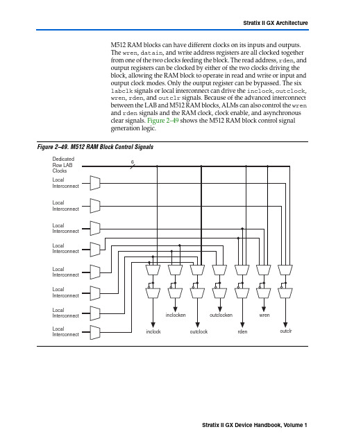
Stratix II GX ArchitectureM512 RAM blocks can have different clocks on its inputs and outputs.The wren, datain, and write address registers are all clocked togetherfrom one of the two clocks feeding the block. The read address, rden, andoutput registers can be clocked by either of the two clocks driving theblock, allowing the RAM block to operate in read and write or input andoutput clock modes. Only the output register can be bypassed. The sixlabclk signals or local interconnect can drive the inclock, outclock,wren, rden, and outclr signals. Because of the advanced interconnectbetween the LAB and M512 RAM blocks, ALMs can also control the wrenand rden signals and the RAM clock, clock enable, and asynchronousclear signals. Figure2–49 shows the M512 RAM block control signalgeneration logic.Figure2–49.M512 RAM Block Control SignalsStratix II GX Device Handbook, Volume 1TransceiversFigure2–4.Transmitter PLL Block Note(1)Note to Figure2–4:(1)The global clock line must be driven by an input pin.The transmitter PLLs support data rates up to 6.375 Gbps. The input clockfrequency is limited to 622.08 MHz. An optional pll_locked port isavailable to indicate whether the transmitter PLL is locked to thereference clock. Both transmitter PLLs have a programmable loopbandwidth parameter that can be set to low, medium, or high. The loopbandwidth parameter can be statically set in the Quartus II software.Table2–2 lists the adjustable parameters in the transmitter PLL.Table2–2.Transmitter PLL SpecificationsParameter SpecificationsInput reference frequency range50 MHz to 622.08 MHzData rate support600 Mbps to 6.375 GbpsMultiplication factor (W)1, 4, 5, 8, 10, 16, 20, 25Bandwidth Low, medium, or highStratix II GX Device Handbook, Volume 1I/O StructureFigure2–75.Stratix II GX Device Fast PLLNotes to Figure2–75:(1)The global or regional clock input can be driven by an output from another PLL, a pin-driven dedicated global orregional clock, or through a clock control block provided the clock control block is fed by an output from another PLL or a pin-driven dedicated global or regional clock. An internally generated global signal cannot drive the PLL.(2)In high-speed differential I/O support mode, this high-speed PLL clock feeds the serializer/deserializer (SERDES)circuitry. Stratix II GX devices only support one rate of data transfer per fast PLL in high-speed differential I/O support mode.(3)This signal is a differential I/O SERDES control signal.(4)Stratix II GX fast PLLs only support manual clock switchover.f Refer to the PLLs in Stratix II & Stratix II GX Devices chapter in volume 2of the Stratix II GX Device Handbook for more information on enhancedand fast PLLs. Refer to “High-Speed Differential I/O with DPA Support”on page2–136 for more information on high-speed differential I/Osupport.I/O Structure The Stratix II GX IOEs provide many features, including:■Dedicated differential and single-ended I/O buffers■ 3.3-V, 64-bit, 66-MHz PCI compliance■ 3.3-V, 64-bit, 133-MHz PCI-X 1.0 compliance■Joint Test Action Group (JTAG) boundary-scan test (BST) support■On-chip driver series termination■On-chip termination for differential standards■Programmable pull-up during configuration■Output drive strength control■Tri-state buffers■Bus-hold circuitry■Programmable pull-up resistors■Programmable input and output delaysStratix II GX Device Handbook, Volume 1。

Key Features• Inverted Video Signals (magnitude increases in a negative direction)• Light source, lens, and sensor are integrated into a single module • 8 dpm resolution• 216 mm scanning length• 0.347ms/line scanning speed, operated @ 5.0MHz • Wide dynamic range Analog output • 660nm light source• Compact size: ≈ 14 mm 19.5 mm x 232 mm • Low power • Light weightGeneral DescriptionThe PI240MC-A4 is a contact imaging sensor, CIS, module, which is composed of 1728PI3020 sensor chips. The PI3020 is a 200 DPI solid-state line imaging array, also a product of Peripheral Imaging Corporation. This imaging device is fabricated using MOS imaging sensor technology for high-speed performance and high sensitivity. The PI240MC-A4 is suitable for scanning A4 size (216 mm) documents with 8 dots per millimeter resolution. Applications include variety of document scanners, variety of mark readers, and other automation equipment.Functional DescriptionThe PI240MC-A4 imaging array consists of 27 chips that are cascaded to provide 1728 photo-detectors with their associated multiplex switches, and a digital shift register that controls its sequential readout. Mounted in the module is one-to-one gradedindexed micro lens array that focuses the scanned documents to image onto itssensing plane. The on-board amplifierprocesses the video signal to produce a sequential stream of video at the video output pin of the PI240MC-A4 module.Figure 1. PI240MC-A4 Cross Section200DPI CIS ModuleEngineering Data SheetPeripheral ImagingCorporationPI240MC-A4GLASS WINDOWDOCUMENT SURFACELIGHT PATH SENSORSPCB L E D B A R R O D L E N SM O D U L E H O U S EINSIDE PICTORIAL OF MODULEIllumination is by means of an integrated LED light source. All components are housed in a small plastic housing which has a cover glass which acts as the focal point for the object being scanned andprotects the imagingarray, micro lensassembly, and LED light source from dust. I/O to the module is the 10-pin connector located on oneend of the module. See Figure 4. The Mechanical Structure.The cross section of thePI240MC-A4 is shown inFigure 1 and the block diagram in Figure 2.Recommended Operating Conditions (25 °C)ItemSymbol Min Typical Max Units Vdd 4.5 5.0 5.5V Idd 243035ma Vn -4.5-5-15V Ivn 568ma VLED 4.5 5.0 5.5V Power SupplyILED 305430560ma Video Output LevelVid 0.81.01.2V Input voltage at digital high Vih Vdd -1.0Vdd -0.5Vdd V Input voltage at digital low Vil 00.8V Clock frequencyF 3.05.0MHz Clock pulse high duty cycle 25%Clock pulse high duration 50ns Integration timeTint (1)0.3460.610.0ms Operating temperatureTop25500CNote (1). Tint is determined by time interval between two start pulses, SP. The longest integration time is determined by the degree of leakage current degradation that can betolerated by the system. A 10ms maximum is a typical rule-of-thumb hence the experienced CIS user can use his discretion in determining the integration time.Figure 2. PI240MC-A4 Module Block DiagramElectro-Optical Characteristics (25° C)Parameter Symbol Parameter Units NoteNumber of photo detectors1728elementsPixel-to-pixel spacing125µmLine scanning rate(1)Tint347µsec@ 5.0 MHzclockfrequency Clock frequency(2)freq 5.0MHzBright output voltage(3)Vp 1.0VoltsBright outputUp<+/-30%nonuniformity(4)Adjacent pixelUadj<25%nonuniformity(5)Dark nonuniformity(6)Ud<100mVDark output voltage(6)Vd<150mVMTF>30%Modulation transferfunction(7)Definition:(1) Tint: line scanning rate or integration time. Tint is determined by the interval of two start pulses (SP).(2) freq is the main clock frequency.(3) Vpavg = ∑ Vp(n)/1728(4) Up = [(Vpmax - Vp) / Vp] x 100% or [(Vp - Vpmin) / Vp] x 100%(5) Upadj = MAX[ | (Vp(n) - Vp(n+l) | / Vp(n)] x 100%Upadj is the nonuniformity percentage of adjacent pixels(6) Ud = Vdmax - VdminVd is the voltage amplitude between the output video's reset level and its dark level. Vdmin is the minimum output with LED light off.Vdmax: maximum output voltage with the LED light off.(7) MTF = [(Vmax - Vmin) / (Vmax + Vmin)] x 100 [%]Vmax: maximum output voltage at 4.0 lp/mmVmin: minimum output voltage at 4.0 lp/mm(8) lp / mm: line pair per mmSwitching Characteristics (250C)Figure 3Symbol Definitions for the Above Timing DiagramItemSymbol Min. TypicalMax. Units Clock cycle time to 0.2 4.0s Clock pulse width tw 50ns Clock duty cycle2575%Prohibit crossing time of Start Pulse tprh 15ns Data setup time tds 20ns Data hold time tdh 20ns Signal delay time tdl 50ns Signal settling timetsh90nsMODULE TIMING DIAGRAMCPSP tds VoutAbsolute Maximum Rating:Parameter Symbols Maximum Rating UnitsPower supply voltageVdd10VIdd30mAVn-15VIn15mAVLED6VILED650ma Input clock pulse (high level)Vih Vdd – 0.5V VInput clock pulse (low level)Vil-0.5VNote (1): These parameters are absolute maximums and should not be used to operate the module.Operating EnvironmentOperating temperature Top0 to 500C Operating humidity Hop10 to 85%Storage temperature Tstg-25 to+750CStorage humidity Hstg10 to 90% Mechanical ConsiderationsI/O Connector Pin configurationConnector is a 1.25mm 10 pin JAE IL-Z-10P-S125L3-E. Its location, along with its pin1 location, are shown in Figure 4 The Mechanical Structure.Pin Number Symbol Names and Functions1Vout Analog video output2Gnd Ground; 0V3Vdd (+5V)Positive power supply4Vn (-5V to –12V)Negative power supply5Gnd Ground; 0V6SP Shift register start pulse7Gnd Ground; 0V8CP Sampling clock pulse9GLED Ground for the light source; 0V10VLED Supply for the light sourceModule Housing DimensionsThe PI240MC-A4 module outline and its mechanical dimensions are shown. A detailed housing drawing is available upon request.ALL DIMENSIONS IN MM UNLESS OTHERWISE SPECIFIEDMECHANICAL STRUCTUREFIGURE 4©2001 Peripheral Imaging Corporation.Printed in USA. All rights reserved. Specificationsare subject to change without notice. Contents may not be reproduced in whole or in part without the express prior written permission of Peripheral Imaging Corporation. Information furnished herein is believed to be accurate and reliable. However, no responsibility is assumed by Peripheral Imaging Corporation for its use nor for any infringement of patents or other rights granted by implication or otherwise under any patent or patent rights of Peripheral Imaging Corporation.。