FQT13N06L中文资料
- 格式:pdf
- 大小:678.22 KB
- 文档页数:8


现货库存、技术资料、百科信息、热点资讯,精彩尽在鼎好!FQT13N06Absolute Maximum Ratings T C= 25°C unless otherwise notedParameterDrain-Source VoltageDrain Current- Continuous (T C = 25°C)- Continuous (T C = 70°C)Drain Current- PulsedGate-Source VoltageSOT-223FQT SeriesGDSNotes:1. Repetitive Rating : Pulse width limited by maximum junction temperature2. L = 12.6mH, I AS = 2.8A, V DD = 25V, R G = 25 Ω, Starting T J = 25°C3. I SD ≤ 13A, di/dt ≤ 300A/us, V DD ≤ BV DSS, Starting T J = 25°C4. Pulse Test : Pulse width ≤300µs, Duty cycle ≤2%5. Essentially independent of operating temperatureDSS GS D ∆BV DSS / ∆T J Breakdown Voltage Temperature CoefficientI D = 250 µA, Referenced to 25°C--0.06--V/°C I DSS Zero Gate Voltage Drain Current V DS = 60 V, V GS = 0 V ----1µA V DS = 48 V, T C = 150°C ----10µA I GSSF Gate-Body Leakage Current, Forward V GS = 25 V, V DS = 0 V ----100nA I GSSRGate-Body Leakage Current, ReverseV GS = -25 V, V DS = 0 V-----100nAOn CharacteristicsV GS(th)Gate Threshold VoltageV DS = V GS , I D = 250 µA 2.0-- 4.0V R DS(on)Static Drain-Source On-Resistance V GS = 10 V, I D = 1.4 A --0.110.14Ωg FSForward TransconductanceV DS = 25 V, I D = 1.4 A--3.0--SDynamic CharacteristicsC iss Input Capacitance V DS = 25 V, V GS = 0 V, f = 1.0 MHz--240310pF C oss Output Capacitance--90120pF C rssReverse Transfer Capacitance--1520pFSwitching Characteristicst d(on)Turn-On Delay Time V DD = 30 V, I D = 6.5 A,R G = 25 Ω--520ns t r Turn-On Rise Time --2560ns t d(off)Turn-Off Delay Time --825ns t f Turn-Off Fall Time --1540ns Q g Total Gate Charge V DS = 48 V, I D = 13 A,V GS = 10 V-- 5.87.5nC Q gs Gate-Source Charge -- 2.0--nC Q gdGate-Drain Charge--2.5--nCDrain-Source Diode Characteristics and Maximum RatingsI S Maximum Continuous Drain-Source Diode Forward Current ---- 2.8A I SM Maximum Pulsed Drain-Source Diode Forward Current----11.2A V SD Drain-Source Diode Forward Voltage V GS = 0 V, I S = 2.8 A ---- 1.5V t rr Reverse Recovery Time V GS = 0 V, I S = 13 A,dI F / dt = 100 A/µs --39--ns Q rrReverse Recovery Charge--40--nC(Note 4)(Note 4, 5)(Note 4, 5)(Note 4)DISCLAIMERFAIRCHILD SEMICONDUCTOR RESERVES THE RIGHT TO MAKE CHANGES WITHOUT FURTHER NOTICE TO ANY PRODUCTS HEREIN TO IMPROVE RELIABILITY, FUNCTION OR DESIGN. FAIRCHILD DOES NOT ASSUME ANY LIABILITY ARISING OUT OF THE APPLICATION OR USE OF ANY PRODUCT OR CIRCUIT DESCRIBED HEREIN;NEITHER DOES IT CONVEY ANY LICENSE UNDER ITS PATENT RIGHTS, NOR THE RIGHTS OF OTHERS.LIFE SUPPORT POLICYFAIRCHILD’S PRODUCTS ARE NOT AUTHORIZED FOR USE AS CRITICAL COMPONENTS IN LIFE SUPPORT DEVICES OR SYSTEMS WITHOUT THE EXPRESS WRITTEN APPROVAL OF FAIRCHILD SEMICONDUCTOR CORPORATION.As used herein:1. Life support devices or systems are devices or systems which, (a) are intended for surgical implant into the body,or (b) support or sustain life, or (c) whose failure to perform when properly used in accordance with instructions for use provided in the labeling, can be reasonably expected to result in significant injury to the user.2. A critical component is any component of a life support device or system whose failure to perform can be reasonably expected to cause the failure of the life support device or system, or to affect its safety or effectiveness.PRODUCT STATUS DEFINITIONS Definition of TermsDatasheet Identification Product Status DefinitionAdvance InformationFormative or In Design This datasheet contains the design specifications for product development. Specifications may change in any manner without notice.PreliminaryFirst ProductionThis datasheet contains preliminary data, andsupplementary data will be published at a later date.Fairchild Semiconductor reserves the right to make changes at any time without notice in order to improve design.No Identification Needed Full ProductionThis datasheet contains final specifications. Fairchild Semiconductor reserves the right to make changes at any time without notice in order to improve design.Obsolete Not In ProductionThis datasheet contains specifications on a product that has been discontinued by Fairchild semiconductor.The datasheet is printed for reference information only.TRADEMARKSThe following are registered and unregistered trademarks Fairchild Semiconductor owns or is authorized to use and is not intended to be an exhaustive list of all such trademarks.STAR*POWER is used under licenseACEx™Bottomless™CoolFET™CROSSVOLT ™DenseTrench™DOME™EcoSPARK™E 2CMOS™EnSigna™FACT™FACT Quiet Series™FAST ®FASTr™FRFET™GlobalOptoisolator™GTO™HiSeC™ISOPLANAR™LittleFET™MicroFET™MicroPak™MICROWIRE™OPTOLOGIC™OPTOPLANAR™PACMAN™POP™Power247™PowerTrench ®QFET™QS™QT Optoelectronics™Quiet Series™SLIENT SWITCHER ®SMART START™STAR*POWER™Stealth™SuperSOT™-3SuperSOT™-6SuperSOT™-8SyncFET™TruTranslation™TinyLogic™UHC™UltraFET ®VCX™。


使用手册ATEQ F6th 系列F620 / F610 / F6701.04 版Reference: RF-28300D-UF6系列使用手册修订由于持续更新,本使用手册中包含的信息,本设备的功能和设计如有更改,将不另行通知。
前言/演示:定义、特点和测量原理(#673) 前面板和界面 (#676)安装/ 配件:气源 (#677)启动 (#678)配件 (#682)选配件 (#683)错误消息 (#684)以 CC/min显示结果 (#687)F610 电子连接器 (#692/1)F620 电子连接器(#692/2)F670 电子连接器(#692/7)气动连接器(#693)参数/ 特殊循环:特殊循环 (#623)服务特殊循环 (#631)程序选择 (#679)程序参数 (#680)测试循环管理 (#681)爆裂测试 (#698)程序功能:功能管理 (#601)名称 (#602)程序链接 (#603)单位 (#604)自动连接器 (#605)测试检查 (#606)ATR (#607)预充气模式和充气模式 (#608) 阀代码 & 24V辅助输出 (#609) 循环结束 (#610)迷你阀 (#611)复工界限 (#612)密封零件 (#613)N 测试 (#614)参考容积 (#615)标记 (#617)温度校正 1 (#618)峰值保持 (#620) 正负号 (#621)过滤 (#622)流量水平 (#624)非负 (#625)绝对值 (#626)显示模式 (#627) 不排气(#630)蜂鸣器 (#639)外部排气 (#655)ATF (#685)隔断 (#686)By pass (#691)配置菜单:日期 / 时间 (#635)语言 (#642)电子调压阀 (#645)调压阀控制 (#646)稳定调压阀 (#647)压力传感器自动归零 (#648)自动短归零 (#649)排气水平 (#651)RS232 (#652)安全性 (#653)I/O 配置 (#654)IN7 测试 (#656)智能键 (#688)压力单位 (#695)USB (#696)结果菜单 / USB 菜单:储存 (#638)阀服务 (#658)I/O服务 (#661)系统信息 (#665)重置参数 (#669)结果菜单 (#689)服务 / USB (#690)CAN 状态 (#697)# 601: 功能管理# 602: 名称# 603: 程序链接# 604: 单位# 605: 自动连接器# 606: 测试检查# 607: ATR# 608: 预充气模式和充气模式# 609: 阀代码 & 24V 辅助输出# 610: 循环结束# 611: 迷你阀# 612: 复工界限# 613: 密封零件# 614: N 测试# 615: 参考容积# 617: 标记# 618: 温度校准 1# 620: 峰值保持# 621: 符号取反# 622: 过滤# 623: 特殊循环# 624: 流量水平# 625: 非负# 626: 绝对值# 627: 显示模式# 631: 服务特殊循环# 635: 日期 / 时间# 638: 储存# 639 : 蜂鸣器# 642: 语言# 645: 电子调压阀# 646: 调压阀控制# 647: 稳定调压阀# 648: 压力传感器自动归零# 649: 自动短归零# 651: 排气水平# 652: RS232# 653: 安全性# 654: I/O 配置# 655 : 外部排气# 656: IN7 测试# 658: 阀服务# 661: I/O 服务# 665: 系统信息# 669: 重置参数# 673: 定义,特性和测试原理# 676: 前面板和界面# 677: 气源# 678: 启动# 679: 程序选择# 680: 程序参数 (Leak)# 681: 测试循环管理# 682: 配件# 683: 选配件# 684: 错误消息# 685: ATF# 686: 隔断# 687: 以CC/min显示结果# 688: 智能键# 689: 结果菜单# 690: 服务 / USB# 691: By pass# 692/1: F610电子连接器# 692/2: F620电子连接器# 692/7: F670 电子连接器# 693: 气动# 695: 压力单位# 696: USB# 697: CAN 状态# 698 : 爆裂测试功能管理扩展菜单功能能够进行个性化设置和添加个人选项到测试循环当中。
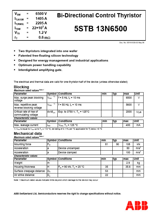
V SM=6500 V I T(AV)M=1405 A I T(RMS)=2205 A I TSM=22×103 A V T0= 1.2 V r T=0.6 mΩBi-Directional Control Thyristor 5STB 13N6500Doc. No. 5SYA1035-03 May 06•Two thyristors integrated into one wafer•Patented free-floating silicon technology•Designed for energy management and industrial applications•Optimum power handling capability•Interdigitated amplifying gate.The electrical and thermal data are valid for one-thyristor-half of the device (unless otherwise stated)BlockingMaximum rated values Note 1Parameter Symbol Conditions min typ max Unit Max. surge peak blockingvoltageV SM1) f = 5 Hz, t p = 10 ms 6500 VMax. repetitive peakreverse blocking voltageV RM1) f = 50 Hz, t p = 10 ms 5600 VCritical rate of rise ofcommutating voltagedv/dt crit Exp. to 3750 V, T vj = 125°C 2000 V/µsCharacteristic valuesParameter Symbol Conditions min typ max UnitMax. leakage current I RM V RM, T vj = 125 °C 400 mA1) V RM is equal to V SM up to T vj = 110 °C; de-rating of 0.11% per °C applicable for Tj below +5 °CMechanical dataMaximum rated values Note 1Parameter Symbol Conditions min typ max UnitMounting force F M 81 90 108 kN Acceleration a Device unclamped 50 m/s2 Acceleration a Device clamped 100 m/s2 Characteristic valuesParameter Symbol Conditions min typ max UnitWeight m 2.9 kg Housing thickness H F M = 90 kN, T a = 25 °C 35 35.6 mm Surface creepage distance D S 53 mm Air strike distance D a 22 mm Note 1 Maximum rated values indicate limits beyond which damage to the device may occur元器件交易网ABB Switzerland Ltd, Semiconductors reserves the right to change specifications without notice.On-stateMaximum rated valuesNote 1ParameterSymbol Conditions mintypmax Unit Average on-state current I T(AV)M Half sine wave, T c = 70 °C 1405 A RMS on-state current I T(RMS)2205 A RMS on-state current I T(RMS) Full sine wave, T c = 70 °C 3120 A Peak non-repetitive surgecurrentI TSM 22.0×10³A Limiting load integral I 2t t p = 10 ms, T vj = 125 °C, sine wave after surge: V D = V R = 0 V2.42×106 A 2s Peak non-repetitive surge currentI TSM 24.0×10³ A Limiting load integralI 2tt p = 8.3 ms, T vj = 125 °C, sine wave after surge: V D = V R = 0 V2.39×106A 2s Characteristic valuesParameter Symbol Conditions mintypmax Unit On-state voltage V T I T = 1500 A, T vj = 125 °C 2.12 V Threshold voltage V T0 1.2 V Slope resistance r T I T = 670 A - 2000 A, T vj = 125 °C0.6 m Ω Holding current I H T vj = 25 °C 300 mAT vj = 125 °C 175 mA Latching current I L T vj = 25 °C 500 mAT vj = 125 °C300mASwitchingMaximum rated valuesNote 1ParameterSymbol Conditions mintypmax Unit Critical rate of rise of on-state currentdi/dt crit Cont. f = 50 Hz 250 A/µs Critical rate of rise of on-state currentdi/dt critT vj = 125 °C, I TRM = 2000 A, V D ≤ 3750 V, I FG = 2 A, t r = 0.5 µsCont. f = 1Hz500 A/µs Circuit commutated turn-off timet q T vj = 125 °C, I TRM = 2000 A, V R = 200 V, di T /dt = -1.5 A/µs, V D ≤ 0.67⋅V RM , dv D /dt = 20V/µs,800µsCharacteristic valuesParameter Symbol Conditions min typmax Unit Recovery charge Q rr 2400 3800 µAs Recovery charge I RM T vj = 125 °C, I TRM = 2000 A, V R = 200 V, di T /dt = -1.5 A/µs 50 70 A Gate turn-on delay timet gdT vj = 25 °C, V D = 0.4⋅V RM , I FG = 2 A, t r = 0.5 µs3µsTriggeringMaximum rated valuesNote 1ParameterSymbol Conditions mintypmax Unit Peak forward gate voltage V FGM 12 V Max. rated peak forwardgate currentI FGM 10 A Peak reverse gate voltage V RGM10 V Max. rated gate power loss P GFor DC gate current3W Max. rated peak forward gate powerP GMsee Fig. 9Characteristic valuesParameter Symbol Conditions mintypmax Unit Gate trigger voltage V GT T vj = 25 °C 2.6 V Gate trigger current I GT T vj = 25 °C400 mA Gate non-trigger voltage V GD V D = 0.4 x V RM , T vj = 125 °C 0.3 V Gate non-trigger current I GDV D = 0.4 x V RM10mAThermalMaximum rated valuesNote 1Parameter Symbol Conditions min typ max Unit Operating junction temperature rangeT vj125 °C Storage temperature range T stg-40 140 °C Characteristic valuesParameterSymbol Conditionsmin typ max Unit R th(j-c) Double-side cooled F m = 81...108 kN 11.4 K/kW R th(j-c)A Anode-side cooled F m = 81...108 kN 22.8 K/kW Thermal resistance junction to case(Valid for one thyristor half no heat flow to the second half.)R th(j-c)C Cathode-side cooled F m = 81...108 kN 22.8K/kW Thermal resistance case to heatsink R th(c-h) Double-side cooled F m = 81...108 kN 2 K/kWR th(c-h)Single-side cooled F m = 81...108 kN4K/kWAnalytical function for transient thermalimpedance:)e -(1R = (t)Z n 1i t/-i c)-th(j ∑=i τi 1 2 3 4 R i (K/kW) 6.770 2.510 1.340 0.780τi (s)0.86510.15580.02120.0075Fig. 1 Transient thermal impedance junction-to caseFig. 2 On-state characteristics,T j = 125°C, 10ms half sine Fig. 3 On-state voltage characteristicsFig. 4 On-state power dissipation vs. mean on-statecurrent. Switching losses excluded.Fig. 5 Max. permissible case temperature vs. meanon-state current. Switching losses ignored.Fig. 6 Surge on-state current vs. pulse length.Half-sine wave.Fig. 7 Surge on-state current vs. number of pulses.Half-sine wave, 10 ms, 50Hz.Fig. 8 Recommended gate current waveformFig. 9 Max. peak gate power lossFig. 10 Recovery charge vs. decay rate of on-statecurrentFig. 11 Peak reverse recovery current vs. decay rateof on-state currentTurn-on and Turn-off lossesFig. 12Turn-on energy, half sinusoidal waves Fig. 13Turn-on energy, rectangular wavesFig. 14Turn-off energy, half sinusoidal waves Fig. 15Turn-off energy, rectangular waves Turn-offABB Switzerland Ltd, Semiconductors reserves the right to change specifications without notice.ABB Switzerland Ltd Doc. No. 5SYA1035-03 May 06Semiconductors Fabrikstrasse 3CH-5600 Lenzburg, SwitzerlandTelephone +41 (0)58 586 1419 Fax +41 (0)58 586 1306Fig. 18 Device Outline DrawingRelated documents:5SYA 2020 Design of RC-Snubber for Phase Control Applications 5SYA 2034 Gate-Drive Recommendations for PCT's5SYA 2036 Recommendations regarding mechanical clamping of Press Pack High Power Semiconductors5SZK 9104 Specification of environmental class for pressure contact diodes, PCTs and GTO, STORAGE available on request, pleasecontact factory5SZK 9105Specification of environmental class for pressure contact diodes, PCTs and GTO, TRANSPORTATION available on request, please contact factoryPlease refer to /semiconductors for actual versions.。


Previous Page | Return to Index | Next PageDIN PLUGS AND RECEPTACLES1. STRAIGHT CORD PLUG with Flush Socket Insert2. STRAIGHT CORD PLUG with Lock Flange3. RECEPTACLE with Extended Shell (57KD5M shown)click here to download a schematic drawing(you will need to have Adobe Acrobat installed on your system to do this)STRAIGHT CORD PLUG with Flush Socket InsertType 04AL2F - typical Female plug with ground contact. Diecast metal shell, nickel-plated. Two contact plug, Part number 04AL2F includes a break circuit switch (1-B) which is opened by engaging the insulated switch actuator of the mating plug or receptacle. Flexible black strain relief.ORDERING INFORMATIONPart Number DescriptionContact Arrangement¤04AL2F 2 contacts with closed-circuit switch (Schematic#4)A¤06AL3F 3 contacts at 180°B06AL5F 5 contacts at 180°F¤10AL4F 4 contacts at 210°D¤13AL5F 5 contacts at 240°E¤13AL6F 6 contacts at 240°G¤15AL7F7 contacts at 270°H15AL8F8 contacts at 270°N STRAIGHT CORD PLUG with Lock FlangeType 06EL5F - typical Female plug with ground contact. Lock flange designed to accept 30° lockring. Insert screw firmly holds insert assembly in shell. Flexible black strain relief with 7/32 inch diameter cable entry. Heavy duty cable clamp.ORDERING INFORMATIONPart Number DescriptionContact Arrangement¤04EL2F 2 contacts with insulated switch actuator A ¤06EL3F 3 contacts at 180°B ¤06EL5F 5 contacts at 180°F13EL5F 5 contacts at 240°E¤15EL7F7 contacts at 270°H¤15EL8F8 contacts at 270°N RECEPTACLE with Extended ShellType 57KD3M - typical Male receptacle, 3 pins, with ground key-rib. Diecast extended shell and flange for chassis or panel mounting. Turret terminals.Part Number DescriptionPin Arrangement57KD3M 3 pins at 180°2¤ Available on special order only; contact Switchcraft for price and delivery.Previous Page | Return to Index | Next PageTo search a category please click on the corresponding icon:| Connectors | Jacks and Plugs || Patch Panels, Patch Kits & Jackfields | Cable Assemblies and Patch Cords | Switches | All products shown are covered by Switchcraft's limited lifetime warranty.| Switchcraft home |About Us | Products | What's New | Search | Contact Us。


现货库存、技术资料、百科信息、热点资讯,精彩尽在鼎好!©2000 Fairchild Semiconductor International Rev. A, April 2000F Q P F 3N 60FQPF3N60600V N-Channel MOSFETGeneral DescriptionThese N-Channel enhancement mode power field effect transistors are produced using Fairchild’s proprietary,planar stripe, DMOS technology.This advanced technology has been especially tailored to minimize on-state resistance, provide superior switching performance, and withstand high energy pulse in the avalanche and commutation mode. These devices are well suited for high efficiency switch mode power supply.TO-220FG SD©2000 Fairchild Semiconductor International FQPF3N60(Note 4)(Note 4, 5)(Note 4, 5) (Note 4)Rev. A, April 2000Electrical Characteristics T C= 25°C unless otherwise notedNotes:1. Repetitive Rating : Pulse width limited by maximum junction temperature2. L = 92mH, I AS = 2.0A, V DD = 50V, R G = 25 Ω, Starting T J = 25°C3. I SD 3.0A, di/dt 200A/µs, V DD BV DSS, Starting T J = 25°C4. Pulse Test : Pulse width 300µs, Duty cycle 2%5. Essentially independent of operating temperatureSymbol Parameter Test Conditions Min Typ Max UnitsOff CharacteristicsBV DSS Drain-Source Breakdown Voltage V GS = 0 V, I D = 250 µA600----V ∆BV DSS / ∆T J Breakdown Voltage Temperature CoefficientI D = 250 µA, Referenced to 25°C --0.6--V/°C I DSS Zero Gate Voltage Drain Current V DS = 600 V, V GS = 0 V ----10µA V DS = 480 V, T C = 125°C ----100µA I GSSF Gate-Body Leakage Current, Forward V GS = 30 V, V DS = 0 V ----100nA I GSSRGate-Body Leakage Current, ReverseV GS = -30 V, V DS = 0 V-----100nAOn CharacteristicsV GS(th)Gate Threshold Voltage V DS = V GS , I D = 250 µA3.0-- 5.0V R DS(on)Static Drain-Source On-ResistanceV GS = 10 V, I D = 1.0 A -- 2.8 3.6Ωg FSForward TransconductanceV DS = 50 V, I D = 1.0 A--2.2--SDynamic CharacteristicsC iss Input Capacitance V DS = 25 V, V GS = 0 V, f = 1.0 MHz--350450pF C oss Output Capacitance--5065pF C rssReverse Transfer Capacitance--5.57.5pFSwitching Characteristicst d(on)Turn-On Delay Time V DD = 300 V, I D = 3.0 A,R G = 25 Ω--1030ns t r Turn-On Rise Time --3070ns t d(off)Turn-Off Delay Time --2050ns t f Turn-Off Fall Time --3070ns Q g Total Gate Charge V DS = 480 V, I D = 3.0 A,V GS = 10 V--1013nC Q gs Gate-Source Charge -- 2.7--nC Q gdGate-Drain Charge--4.9--nCDrain-Source Diode Characteristics and Maximum RatingsI S Maximum Continuous Drain-Source Diode Forward Current ---- 2.0A I SM Maximum Pulsed Drain-Source Diode Forward Current----8.0A V SD Drain-Source Diode Forward Voltage V GS = 0 V, I S = 2.0 A ---- 1.4V t rr Reverse Recovery Time V GS = 0 V, I S = 3.0 A,dI F / dt = 100 A/µs--210--ns Q rrReverse Recovery Charge-- 1.2--µC©2000 Fairchild Semiconductor International F Q P F 3N 60Rev. A, April 2000©2000 Fairchild Semiconductor InternationalFQPF3N60Rev. A, April 2000©2000 Fairchild Semiconductor International F Q P F 3N 60Rev. A, April 2000©2000 Fairchild Semiconductor International FQPF3N60Rev. A, April 2000©2000 Fairchild Semiconductor InternationalF Q P F 3N 60Rev. A, April 2000TRADEMARKSThe following are registered and unregistered trademarks Fairchild Semiconductor owns or is authorized to use and is not intended to be an exhaustive list of all such trademarks.ACEx™Bottomless™CoolFET™CROSSVOLT™E2CMOS™FACT™FACT Quiet Series™FAST®FASTr™GTO™HiSeC™ISOPLANAR™MICROWIRE™POP™PowerTrench®QFET™QS™Quiet Series™SuperSOT™-3SuperSOT™-6SuperSOT™-8SyncFET™TinyLogic™UHC™VCX™DISCLAIMERFAIRCHILD SEMICONDUCTOR RESERVES THE RIGHT TO MAKE CHANGES WITHOUT FURTHER NOTICE TO ANY PRODUCTS HEREIN TO IMPROVE RELIABILITY, FUNCTION OR DESIGN. FAIRCHILD DOES NOT ASSUME ANY LIABILITY ARISING OUT OF THE APPLICATION OR USE OF ANY PRODUCT OR CIRCUIT DESCRIBED HEREIN; NEITHER DOES IT CONVEY ANY LICENSE UNDER ITS PATENT RIGHTS, NOR THE RIGHTS OF OTHERS.LIFE SUPPORT POLICYFAIRCHILD’S PRODUCTS ARE NOT AUTHORIZED FOR USE AS CRITICAL COMPONENTS IN LIFE SUPPORT DEVICES OR SYSTEMS WITHOUT THE EXPRESS WRITTEN APPROVAL OF FAIRCHILD SEMICONDUCTOR INTERNATIONAL.As used herein:1. Life support devices or systems are devices or systems which, (a) are intended for surgical implant into the body, or (b) support or sustain life, or (c) whose failure to perform when properly used in accordance with instructions for use provided in the labeling, can be reasonably expected to result in significant injury to the user.2. A critical component is any component of a life support device or system whose failure to perform can be reasonably expected to cause the failure of the life support device or system, or to affect its safety or effectiveness.PRODUCT STATUS DEFINITIONSDefinition of TermsDatasheet Identification Product Status DefinitionAdvance Information Formative or InDesign This datasheet contains the design specifications for product development. Specifications may change in any manner without notice.Preliminary First Production This datasheet contains preliminary data, andsupplementary data will be published at a later date.Fairchild Semiconductor reserves the right to makechanges at any time without notice in order to improvedesign.No Identification Needed Full Production This datasheet contains final specifications. FairchildSemiconductor reserves the right to make changes atany time without notice in order to improve design.Obsolete Not In Production This datasheet contains specifications on a productthat has been discontinued by Fairchild semiconductor.The datasheet is printed for reference information only.©2000 Fairchild Semiconductor International Rev. A, January 2000。


NB6L142.5 V/3.3 V 3.0 GHz Differential 1:4 LVPECL Fanout BufferMulti−Level Inputs with Internal TerminationDescriptionThe NB6L14 is a 3.0 GHz differential 1:4 LVPECL clock or data fanout buffer. The differential inputs incorporate internal 50 W termination resistors that are accessed through the VT pin. This feature allows the NB6L14 to accept various logic standards, such as LVPECL, LVCMOS, LVTTL, CML, or LVDS logic levels. The VREF_AC reference output can be used to rebias capacitor−coupled differential or single−ended input signals. The 1:4 fanout design was optimized for low output skew applications.The NB6L14 is a member of the ECLinPS MAX™ family of high performance clock and data management products.Features•Input Clock Frequency > 3.0 GHz•Input Data Rate > 2.5 Gb/s•< 20 ps Within Device Output Skew•350 ps Typical Propagation Delay•150 ps Typical Rise and Fall Times•Differential LVPECL Outputs, 700 mV Amplitude, Typical •LVPECL Mode Operating Range: V CC = 2.375 V to 3.63 V with GND = 0 V•Internal 50 W Input Termination Resistors Provided •VREF_AC Reference Output V oltage•−40°C to +85°C Ambient Operating Temperature •Available in 3 mm x 3 mm 16 Pin QFN•These are Pb−Free DevicesMARKINGDIAGRAM*QFN−16MN SUFFIXCASE 485GA= Assembly LocationL= Wafer LotY= YearW= Work WeekG= Pb−Free Package(Note: Microdot may be in either location)1*For additional marking information, refer toApplication Note AND8002/D.See detailed ordering and shipping information in the package dimensions section on page 9 of this data sheet.ORDERING INFORMATIONFigure 1. Simplified Logic DiagramINVTINCCQ0Q0V Q2Exposed Pad (EP)Figure 2. QFN −16 Pinout(Top View)GND Q3Q2Q1Q1Figure 3. Logic DiagramTable 1. EN TRUTH TABLEIN IN EN Q0:Q3Q0:Q301x10x110010+101++ = On next negative transition of the input signal (IN).x = Don’t care.Table 2. PIN DESCRIPTIONPin Name I/O Description1Q1LVPECL Output Non −inverted Differential Output. Typically Terminated with 50 W Resistor to V CC –2.0 V.2Q1LVPECL Output Inverted Differential Output. Typically Terminated with 50 W Resistor to V CC – 2.0 V.3Q2LVPECL Output Non −inverted Differential Output. Typically Terminated with 50 W Resistor to V CC – 2.0 V.4Q2LVPECL Output Inverted Differential Output. Typically Terminated with 50 W Resistor to V CC – 2.0 V.5Q3LVPECL Output Non −inverted Differential Output. Typically Terminated with 50 W Resistor to V CC – 2.0 V.6Q3LVPECL OutputInverted Differential Output. Typically Terminated with 50 W Resistor to V CC – 2.0 V.7V CC −Positive Supply Voltage8ENLVTTL/LVCMOSSynchronous Output Enable. When LOW, Q outputs will go LOW and Q outputs will go HIGH on the next negative transition of IN input. The internal DFF register is clocked on the falling edge of IN input (see Figure 20). The EN pin has an internal pullup resistor and defaults HIGH when left open.9IN LVPECL, CML,LVDS, HSTLInverted Differential Clock Input. Internal 50 W Resistor to Termination Pin, VT.10VREF_ACOutput Voltage Reference for capacitor −coupled inputs, only.11VT Internal 100 W center −tapped Termination Pin for IN and IN.12IN LVPECL, CML,LVDS, HSTLNon −inverted Differential Clock Input. Internal 50 W Resistor to Termination Pin, VT.13GND −Negative Supply Voltage 14V CC −Positive Supply Voltage15Q0LVPECL Output Noninverted Differential Output. Typically Terminated with 50 W Resistor to V CC –2.0 V.16Q0LVPECL OutputInverted Differential Output. Typically Terminated with 50 W Resistor to V CC –2.0 V.−EP−The Exposed Pad (EP) on the QFN −16 package bottom is thermally connected to the die for improved heat transfer out of package. The exposed pad must be attached to a heat −sinking conduit. The pad is not electrically connected to the die, but isrecommended to be electrically and thermally connected to GND on the PC board.1.In the differential configuration when the input termination pin VT , is connected to a common termination voltage or left open, and if no signal is applied on IN/IN inputs, then the device will be susceptible to self −oscillation.Table 3. ATTRIBUTESCharacteristics ValueESD Protection Human Body ModelMachine Model > 4 kV > 100 VMoisture Sensitivity (Note 2)QFN−16Level 1Flammability Rating Oxygen Index: 28 to 34UL 94 V−0 @ 0.125 inTransistor Count167Meets or exceeds JEDEC Spec EIA/JESD78 IC Latchup Test2.For additional information, see Application Note AND8003/D.Table 4. MAXIMUM RATINGSSymbol Parameter Condition 1Condition 2Rating Unit V CC Positive Power Supply GND = 0 V 4.0VV Io Positive Input/Output GND = 0 V−0.5 V v V Io v V CC+ 0.5 V 4.0VI IN Input CurrentSource or Sink Current (IN/IN)"50mA I VREF_AC Source or Sink Current on VT Pin"2.0mAI OUT Output Current ContinuousSurge 50100mAmAT A Operating Temperature Range−40 to +85°C T stg Storage Temperature Range−65 to +150°Cq JA Thermal Resistance(Junction−to−Ambient) (Note 3)0 lfpm500 lfpmQFN−16QFN−164235°C/W°C/Wq JC Thermal Resistance (Junction−to−Case)(Note 3)QFN−164°C/W T sol Wave Solder Pb−Free265°C Stresses exceeding Maximum Ratings may damage the device. Maximum Ratings are stress ratings only. Functional operation above the Recommended Operating Conditions is not implied. Extended exposure to stresses above the Recommended Operating Conditions may affect device reliability.3.JEDEC standard multilayer board − 2S2P (2 signal, 2 power) with 8 filled thermal vias under exposed pad.Table 5. DC CHARACTERISTICS, Multi−Level Inputs, LVPECL OutputsV CC= 2.375 V to 3.63 V, GND = 0 V, T A = −40°C to +85°CSymbol Characteristic Min Typ Max Unit I CC Power Supply Current (Inputs and Outputs Open)354765mA LVPECL OUTPUT DC ELECTRICAL CHARACTERISTICSV OH Output HIGH Voltage (Notes 4 and 5) (Q, Q)V CC = 3.3 VV CC = 2.5 V V CC− 114521551355V CC− 102022801480V CC− 89524051605mVV OL Output LOW Voltage (Notes 4 and 5) (Q, Q)V CC = 3.3 VV CC = 2.5 V V CC− 19451355555V CC− 18751475675V CC− 16951605805mVDIFFERENTIAL INPUT DRIVEN SINGLE−ENDED (See Figures 10 and 11)V th Input Threshold Reference Voltage Range (Note 6)1100V CC− 100mVV IH Single−Ended Input High Voltage V th + 100V CC mVV IL Single−Ended Input LOW Voltage GND V th− 100mVV ISE Single−Ended Input Voltage Amplitude (V IH− V IL)200V CC− GND mVV REFACV REFAC Output Reference Voltage (V CC w 2.5 V)V CC− 1.525V CC− 1.425V CC− 1.325mV DIFFERENTIAL INPUTS DRIVEN DIFFERENTIALLY (See Figures 12 and 13) (Note 7)V IHD Differential Input HIGH Voltage1200V CC mVV ILD Differential Input LOW Voltage GND V IHD− 100mVV CMR Input Common Mode Range (Differential Configuration)(Note 8)950V CC – 50mVV ID Differential Input Voltage (IN−IN) (V IHD−V ILD)100V CC− GND mVI IH Input HIGH Current IN/IN(VT Open)−150+150m AI IL Input LOW Current IN/IN(VT Open)−150+150m A LVTTL/LVCMOS INPUT DC ELECTRICAL CHARACTERISTICSV IH Input HIGH Voltage 2.0V CC VV IL Input LOW Voltage GND0.8VI IH Input HIGH Current, V CC = V IN = 3.63 V−1050m AI IL Input LOW Current, V CC = 3.63 V, V IN = 0 V−1500m A TERMINATION RESISTORSR TIN Internal Input Termination Resistor (IN to VT)405060WR DIFF_IN Differential Input Resistance (IN to IN)80100120W NOTE:Device will meet the specifications after thermal equilibrium has been established when mounted in a test socket or printed circuit board with maintained transverse airflow greater than 500 lfpm. Electrical parameters are guaranteed only over the declaredoperating temperature range. Functional operation of the device exceeding these conditions is not implied. Device specification limit values are applied individually under normal operating conditions and not valid simultaneously.4.LVPECL outputs loaded with 50 W to V CC− 2.0 V for proper operation.5.Input and output parameters vary 1:1 with V CC.6.V th is applied to the complementary input when operating in single−ended mode.7.V IHD, V ILD, V ID and V CMR parameters must be complied with simultaneously.8.V CMR min varies 1:1 with GND, V CMR max varies 1:1 with V CC. The V CMR range is referenced to the most positive side of the differentialinput signal.Table 6. AC CHARACTERISTICS V CC = 2.375 V to 3.63 V, GND = 0 V, T A = −40°C to +85°C (Note 9)Symbol CharacteristicMin Typ MaxUnit V OUTPPOutput Voltage Amplitude (@ V INPPmin ) (Note 10)f IN ≤ 1.25 GHz1.25 GHz ≤ f in ≤2.0 GHz 2.0 GHz ≤ f in ≤3.0 GHz 550380250700500320mVf DATA Maximum Operating Data Rate 2.5Gb/s t PD Propagation Delay IN to Q 250370500ps t S Set −Up Time (Note 11)EN to IN, IN 300ps t H Hold Time (Note 11)EN to IN, IN300ps t SKEWWithin −Device Skew (Note 12)Device to Device Skew (Note 13)5.020150pst JITTERRMS Random Jitter (Note 14)f IN = 2.5 GHz Peak −to −Peak Data Dependent Jitter (Note 15)f DATA = 2.5 Gb/s141.0psV INPP Input Voltage Swing/Sensitivity(Differential Configuration) (Note 10)100V CC − GNDmV t r ,t fOutput Rise/Fall Times @ Full Output Swing (20%−80%)70150200psNOTE:Device will meet the specifications after thermal equilibrium has been established when mounted in a test socket or printed circuitboard with maintained transverse airflow greater than 500 lfpm. Electrical parameters are guaranteed only over the declaredoperating temperature range. Functional operation of the device exceeding these conditions is not implied. Device specification limit values are applied individually under normal operating conditions and not valid simultaneously.9.Measured by forcing V INPP (min) from a 50% duty cycle clock source. All loading with an external R L = 50 W to V CC – 2.0 V. Input edge rates 40 ps (20%−80%).10.Input and output voltage swing is a single −ended measurement operating in differential mode.11.Set −up and hold times apply to synchronous applications that intend to enable/disable before the next clock cycle. For asynchronous applications, set −up and hold times do not apply.12.Within device skew is measured between two different outputs under identical power supply, temperature and input conditions.13.Device to device skew is measured between outputs under identical transition @ 0.5 GHz.14.Additive RMS jitter with 50% duty cycle clock signal.15.Additive peak −to −peak data dependent jitter with input NRZ data at PRBS 2^23−1 and K28.5 at 2.5Gb/s.80070060050040030020010000123f out , CLOCK OUTPUT FREQUENCY (GHz)V O U T P P O U T P U T V O L T A G E A M P L I T U D E (m V )(T Y P I C A L )Figure 4. Output Voltage Amplitude (V OUTPP ) versus OutputFrequency at Ambient Temperature (Typical)Figure 5. Typical Phase Noise Plot atf carrier = 311.04 MHz Figure 6. Typical Phase Noise Plot atf carrier = 622.08 MHzFigure 7. Typical Phase Noise Plot atf carrier = 1 GHz Figure 8. Typical Phase Noise Plot atf carrier= 2 GHzThe above phase noise plots captured using AgilentE5052A show additive phase noise of the NB6L14 device atfrequencies 311.04 MHz, 622.08 MHz, 1 GHz and 2 GHzrespectively at an operating voltage of 3.3 V in roomtemperature. The RMS Phase Jitter contributed by thedevice (integrated between 12 kHz and 20 MHz; as shownin the shaded region of the plot) at each of the frequenciesis 27 fs, 17 fs, 13 fs and 5 fs respectively. The input sourceused for the phase noise measurements is Agilent E8663B.Figure 9. Input StructureINthFigure 10. Differential Input DrivenSingle−EndedV IHmax V ILmax V IHV thV ILV IHmin V ILminFigure 11. V thDiagram Figure 12. Differential InputsDriven DifferentiallyV ILV IH(MAX)V IHV ILV IHV IL(MIN)V CMRGNDID = V IHD− V ILDV CCFigure 13. V CMR DiagramININQQ OH(Q) − V OL(Q)IH(IN) − V IL(IN)Figure 14. AC Reference MeasurementFigure 15. LVPECL Interface Figure 16. LVDS InterfaceFigure 17. Standard 50 W Load CML InterfaceFigure 18. Capacitor−CoupledDifferential Interface(VT Connected to V REFAC)*V REFAC bypassed to ground with a 0.01 m F capacitor Figure 19. Capacitor−Coupled Single−Ended Interface (VT Connected to V REFAC)/IN IN /QQOUTPPFigure 21. Typical Termination for Output Driver and Device Evaluation (See Application Note AND8020/D − Termination of ECL Logic Devices.)V TTV TT = V CC − 2.0 VORDERING INFORMATIONDevicePackage Shipping †NB6L14MNG QFN −16, 3x3 mm(Pb −Free)123 Units / Rail NB6L14MNR2GQFN −16, 3x3 mm(Pb −Free)3000 / Tape & Reel†For information on tape and reel specifications, including part orientation and tape sizes, please refer to our Tape and Reel Packaging Specifications Brochure, BRD8011/D.PACKAGE DIMENSIONSQFN16 3x3, 0.5PCASE 485G−01ISSUE FNOTES:1.DIMENSIONING AND TOLERANCING PERASME Y14.5M, 1994.2.CONTROLLING DIMENSION: MILLIMETERS.3.DIMENSION b APPLIES TO PLATEDTERMINAL AND IS MEASURED BETWEEN0.25 AND 0.30 MM FROM TERMINAL.4.COPLANARITY APPLIES TO THE EXPOSEDPAD AS WELL AS THE TERMINALS.L1DETAIL ALALTERNATE TERMINALCONSTRUCTIONSDETAIL BALTERNATECONSTRUCTIONS*For additional information on our Pb−Free strategy and solderingdetails, please download the ON Semiconductor Soldering andMounting Techniques Reference Manual, SOLDERRM/D.RECOMMENDEDDIMENSIONS: MILLIMETERS16X2XSOLDERING FOOTPRINT*DIM MIN NOM MAXMILLIMETERSA0.800.90 1.00A10.000.030.05A30.20 REFb0.180.240.30D 3.00 BSCD2 1.65 1.75 1.85E 3.00 BSCE2 1.65 1.75 1.85e0.50 BSCK0.18 TYPL0.300.400.50L10.000.080.15ON Semiconductor and are registered trademarks of Semiconductor Components Industries, LLC (SCILLC). SCILLC reserves the right to make changes without further notice to any products herein. SCILLC makes no warranty, representation or guarantee regarding the suitability of its products for any particular purpose, nor does SCILLC assume any liability arising out of the application or use of any product or circuit, and specifically disclaims any and all liability, including without limitation special, consequential or incidental damages.“Typical” parameters which may be provided in SCILLC data sheets and/or specifications can and do vary in different applications and actual performance may vary over time. All operating parameters, including “Typicals” must be validated for each customer application by customer’s technical experts. SCILLC does not convey any license under its patent rights nor the rights of others. SCILLC products are not designed, intended, or authorized for use as components in systems intended for surgical implant into the body, or other applications intended to support or sustain life, or for any other application in which the failure of the SCILLC product could create a situation where personal injury or death may occur. Should Buyer purchase or use SCILLC products for any such unintended or unauthorized application, Buyer shall indemnify and hold SCILLC and its officers, employees, subsidiaries, affiliates, and distributors harmless against all claims, costs, damages, and expenses, and reasonable attorney fees arising out of, directly or indirectly, any claim of personal injury or death associated with such unintended or unauthorized use, even if such claim alleges that SCILLC was negligent regarding the design or manufacture of the part. SCILLC is an Equal Opportunity/Affirmative Action Employer. This literature is subject to all applicable copyright laws and is not for resale in any manner.PUBLICATION ORDERING INFORMATIONECLinPS MAX is a trademark of Semiconductor Components Industries, LLC (SCILLC).分销商库存信息: ONSEMINB6L14MNG。
