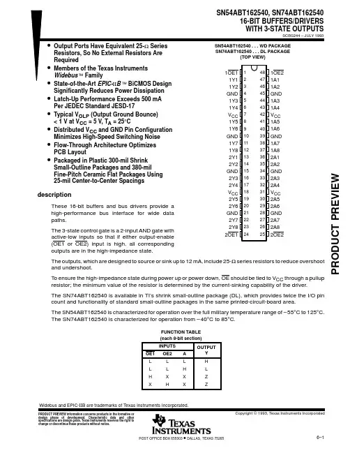
SN74CBT16211CDL中文资料
- 格式:pdf
- 大小:241.52 KB
- 文档页数:14
SN74CBT16211C24ĆBIT FET BUS SWITCH5ĆV BUS SWITCH WITH ć2ĆV UNDERSHOOT PROTECTIONSCDS116C − JANUARY 2003 − REVISED OCTOBER 2003
1POST OFFICE BOX 655303 • DALLAS, TEXAS 75265
DMember of the Texas Instruments
Widebus FamilyDUndershoot Protection for Off-Isolation on
A and B Ports Up To −2 VDBidirectional Data Flow, With Near-Zero
Propagation DelayDLow ON-State Resistance (r
on)
Characteristics (ron = 3 Ω Typical)DLow Input/Output Capacitance Minimizes
Loading and Signal Distortion(Cio(OFF) = 5.5 pF Typical)
DData and Control Inputs Provide
Undershoot Clamp DiodesDLow Power Consumption
(ICC = 3 µA Max)DV
CC Operating Range From 4 V to 5.5 V
DData I/Os Support 0 to 5-V Signaling Levels
(0.8-V, 1.2-V, 1.5-V, 1.8-V, 2.5-V, 3.3-V, 5-V)DControl Inputs Can Be Driven by TTL or
5-V/3.3-V CMOS OutputsDI
off Supports Partial-Power-Down Mode
OperationDLatch-Up Performance Exceeds 100 mA Per
JESD 78, Class IIDESD Performance Tested Per JESD 22
− 2000-V Human-Body Model(A114-B, Class II)− 1000-V Charged-Device Model (C101)DSupports Both Digital and Analog
Applications: PCI Interface, MemoryInterleaving, Bus Isolation, Low-DistortionSignal Gating
description/ordering informationORDERING INFORMATIONTAPACKAGE†ORDERABLEPART NUMBERTOP-SIDEMARKING
TubeSN74CBT16211CDLSSOP − DLTape and reelSN74CBT16211CDLRCBT16211C
°°TubeSN74CBT16211CDGG−40C to 85CTSSOP − DGGTape and reelSN74CBT16211CDGGRCBT16211C
TVSOP − DGVTape and reelSN74CBT16211CDGVRCY211C†Package drawings, standard packing quantities, thermal data, symbolization, and PCB design
guidelines are available at www.ti.com/sc/package.
Copyright 2003, Texas Instruments Incorporated
DGG, DGV, OR DL PACKAGE(TOP VIEW)
1234567891011121314151617181920212223242526272856555453525150494847464544434241403938373635343332313029
NC1A11A21A31A41A51A6GND1A71A81A91A101A111A122A12A2VCC2A3GND2A42A52A62A72A82A92A102A112A121OE2OE1B11B21B31B41B5GND1B61B71B81B91B101B111B122B12B22B3GND2B42B52B62B72B82B92B102B112B12
NC − No internal connection
Please be aware that an important notice concerning availability, standard warranty, and use in critical applications ofTexasInstruments semiconductor products and disclaimers thereto appears at the end of this data sheet.
PRODUCTION DATA information is current as of publication date.Products conform to specifications per the terms of Texas Instrumentsstandard warranty. Production processing does not necessarily includetesting of all parameters.
Widebus is a trademark of Texas Instruments.
元器件交易网www.cecb2b.comSN74CBT16211C24ĆBIT FET BUS SWITCH5ĆV BUS SWITCH WITH ć2ĆV UNDERSHOOT PROTECTIONSCDS116C − JANUARY 2003 − REVISED OCTOBER 2003
2POST OFFICE BOX 655303 • DALLAS, TEXAS 75265
description/ordering information (continued)The SN74CBT16211C is a high-speed TTL-compatible FET bus switch with low ON-state resistance (ron),allowing for minimal propagation delay. Active Undershoot-Protection Circuitry on the A and B ports of theSN74CBT16211C provides protection for undershoot up to −2 V by sensing an undershoot event and ensuringthat the switch remains in the proper OFF state.
The SN74CBT16211C is organized as two 12-bit bus switches with separate output-enable (1OE, 2OE) inputs.It can be used as two 12-bit bus switches or as one 24-bit bus switch. When OE is low, the associated 12-bitbus switch is ON, and the A port is connected to the B port, allowing bidirectional data flow between ports. WhenOE is high, the associated 12-bit bus switch is OFF, and the high-impedance state exists between the A andB ports.
This device is fully specified for partial-power-down applications using Ioff. The Ioff feature ensures that
damaging current will not backflow through the device when it is powered down. The device has isolation duringpower off.
To ensure the high-impedance state during power up or power down, OE should be tied to VCC through a pullupresistor; the minimum value of the resistor is determined by the current-sinking capability of the driver.
FUNCTION TABLE(each 12-bit bus switch)
INPUTOEINPUT/OUTPUTAFUNCTION
LBA port = B portHZDisconnect
logic diagram (positive logic)
1A1SW1B11A121OESW1B12
2A1SW2B12A122OESW2B12
21456
15285554424129
元器件交易网www.cecb2b.com