SMCJ120A中文资料
- 格式:pdf
- 大小:108.51 KB
- 文档页数:4
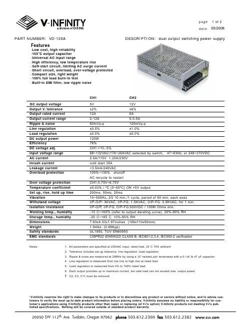
Features·Low cost, high reliability·105°C output capacitor·Universal AC input range·High efficiency, low temperature rise·Soft-start circuit, limiting AC surge current·Short circuit, overload, over-voltage protected·Compact size, light weight·100% full load burn-in test·Built-in EMI filter, low ripple noiseCH1CH2DC output voltage5V12VOutput V.tolerance±2%±6%Output rated current12A5AOutput current range2-12A0.5-5ARipple & noise60mVp-p120mVp-pLine regulation±0.5%±1.0%Load regulation±0.5%±5.0%DC output power120WEfficiency78%DC voltage adj.CH1:+10,-5%Input voltage range88~132VAC/176~264VAC selected by switch, 47~63Hz; or 248~370VDCAC current 2.5A/115V 1.25A/230VInrush current cold start 35ALeakage current<3.5mA/240VACOverload protection105%~135% shutoffAC recycle to restartOver voltage protection CH1:5.75V~6.75VTemperature coefficient±0.03% / ºC (0~50ºC) ON +5V outputSet up, rise, hold up time200ms, 50ms, 20msVibration10~500Hz, 2G 10 min./1 cycle, period of 60 min. each axesWithstand voltage I/P-O/P: 3KVAC, I/P-FG: 1.5KVAC, O/P-FG: 0.5KVAC, for 1 min.Isolation resistance I/P-O/P, I/P-FG, O/P-FG:500VDC / 100M Ohms min.Working temp., humidity-10°C~+60% (refer to output derating curve), 20%-90% RHStorage temp., humidity-20°C~+85°C, 10%-95% RHDimensions7.83x4.33x1.97inches (199x110x50mm)Weight 1.94lbs. (0.88Kgs)Safety standards UL1950, TUV EN60950EMC standards CISPR22 (EN55022) CLASS B, IEC801-2,3,4, IEC555-2 verificationNotes: 1. All parameters are specified at 230VAC input, rated load, 25°C 70% ambient2. Tolerance includes set up tolerance, line regulation, load regulation3. Ripple & noise are measured at 20MHz by using a 12” twisted pair terminated with a 0.1uF & 47 uF capacitor4. Line regulation is measured from low line to high line at rated load5. Load regulation is measured from 0% to 100% rated load6. Each output provides up to maximum current, but total load can not exceed max. output power7. C2, C3, C11 must be removed*V-Infinity reserves the right to make changes to its products or to discontinue any product or service without notice, and to advise cus-tomers to verify the most up-to-date product information before placing orders. V-Infinity assumes no liability or responsibility for cus-tomer’s applications using V-Infinity products other than repair or replacing (at V-I’s option) V-Infinity products not meeting V-I’s pub-lished specifications. Nothing will be covered outside of standard product warranty.Block DiagramOutput DeratingDimensions (mm)。

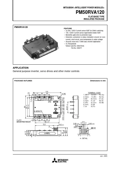
INSULATED PACKAGEConditionParameterSymbol V CES ±I C ±I CP P C T jCollector-Emitter Voltage Collector CurrentCollector Current (Peak)Collector Dissipation Junction TemperatureV D = 15V, V CIN = 15V T C = 25°C T C = 25°C T C = 25°CV A A W °CMAXIMUM RATINGS (Tj = 25°C, unless otherwise noted)INVERTER PARTSymbol ParameterConditionRatings Unit 120050100338–20 ~ +150INTERNAL FUNCTIONS BLOCK DIAGRAMV CES I C I CP P CV R(DC)I F T jBRAKE PARTCollector-Emitter Voltage Collector CurrentCollector Current (Peak)Collector DissipationFWDi Rated DC Reverse Voltage FWDi Forward Current Junction TemperatureV D = 15V, V CIN = 15V T C = 25°C T C = 25°C T C = 25°C T C = 25°C T C = 25°CV A A W V A °CSymbol ParameterConditionRatings Unit 12001530134120015–20 ~ +150V FO I FOCONTROL PARTV mA2020Supply Voltage Input VoltageFault Output Supply Voltage Fault Output CurrentRatings Unit Applied between :V UP1-V UPCV VP1-V VPC , V WP1-V WPC , V N1-V NCApplied between :U P -V UPC , V P -V VPCW P -V WPC , U N • V N • W N • B r -V NCApplied between :U FO -V UPC, V FO-V VPC, W FO -V WPCF O -V NCSink current at U FO , V FO , W FO and F O terminal2020V D V CIN V V GND GND SiOutIn F O V CCGND GND SiOutIn F O V CC GND GND SiOutIn F O V CCGND GND SiOutIn F O V CCF O Br V NC W NV NU NV N1PU V W N B TEMPV WPC W P V WP1GND In V CCGND Si OUTW FO F OV VPC V P V VP1GND In V CCGND Si OUTV FO F OV UPC U P V UP1GND In V CCGND Si OUTU FOF ORfoRfoRfoRfoR fo = 1.5k ΩINSULATED PACKAGETOTAL SYSTEM3.303.353.52.30.31.03.41.2110Min.Typ.Max.Collector-Emitter Saturation Voltage Collector-Emitter Cutoff Current–I C = 50A, V D = 15V, V CIN = 15V T j = 25°C T j = 125°C ELECTRICAL CHARACTERISTICS (Tj = 25°C, unless otherwise noted)INVERTER PARTParameterSymbol Test ConditionV CE(sat)I CESV EC t on t rr t c(on)t off t c(off)Limits ———0.4——————2.652.752.50.90.20.42.40.7——T j = 25°C T j = 125°CFWDi Forward VoltageSwitching TimeV D = 15V, V CIN = 0V ↔15V V CC = 600V, I C = 50A T j = 125°CInductive Load (upper and lower arm)V CE = V CES , V CIN = 15VV D = 15V, I C =50A V CIN = 0VV mAVµsUnit ParameterSymbolSupply Voltage Protected bySCSupply Voltage (Surge)Module Case OperatingTemperatureStorage Temperature Isolation Voltage ConditionV CC(surge)T CT stgV iso Ratings V CC(PROT)8001000–20 ~ +100–40 ~ +1252500Unit V °C °C V rmsV V D = 13.5 ~ 16.5V, Inverter Part,T j = 125°C StartApplied between : P-N, Surge value or without switching(Note-1)60Hz, Sinusoidal, Charged part to Base, AC 1 min.—————V CE(sat)I CESV FM V mAMin.Typ.Max.V Collector-Emitter Saturation Voltage FWDi Forward Voltage Collector-Emitter Cutoff CurrentI F = 15AT j = 25°C T j = 125°CUnit ParameterSymbol Test ConditionLimits 3.303.203.501102.502.202.50——T j = 25°C T j = 125°C BRAKE PARTV D = 15V, I C = 15A V CIN = 0V V CE = V CES , V CIN = 15V(Note-1)T C measurement point is below. (3mm depth at the center of the side of base plate)TcINSULATED PACKAGE3.53.5————Mounting part screw : M5Main terminalscrew : M5—Symbol ParameterMounting torque Mounting torque WeightTest ConditionUnit N • m N • m gLimits Min.Typ.Max.2.52.5—3.03.0560MECHANICAL RATINGS AND CHARACTERISTICS(Note-2)Fault output is given only when the internal SC, OT & UV protection.Fault output of OT protection operate by lower arm.Fault output of OT, UV protection given pulse while over level.V D = 15VBase-plateTemperature detection, V D = 15V –20 ≤ T j ≤ 125°C V D = 15V, V FO = 15V (Note-2)V D = 15V(Note-2)Trip level Reset level Trip level Reset levelCircuit CurrentInput ON Threshold Voltage Input OFF Threshold Voltage Over Current Trip Level Short Circuit Trip Level Over Current Delay Time Short Circuit Current Delay TimeOver Temperature Protection Supply Circuit Under-Voltage ProtectionFault Output Current Minimum Fault Output Pulse WidthV th(ON)V th(OFF)OC SC t off(OC)t off(SC)OT OT r UV UV r I FO(H)I FO(L)t FO–20 ≤ T j ≤ 125°C, V D = 15V, Break part –20≤ T j ≤ 125°C, V D = 15V V D = 15V, Break part Inverter part Brake partCONTROL PARTI D ParameterSymbol µs °C V mA ms60181.82.3—————125—12.5—0.0115—mA ——1.21.72259———111—11.5———1.0Max.Min.Typ.Unit Limits 44131.52.0——52101011810012.012.5—101.8V µs A A V D = 15V, V CIN = 15VApplied between :U P -V UPC , V P -V VPC , W P -V WPCU N • V N • W N • B r -V NC Test ConditionV N1-V NC V *P1-V *PCR th(j-c)Q R th(j-c)F R th(j-c)Q R th(j-c)F R th(c-f)Symbol THERMAL RESISTANCES0.370.700.931.500.027°C/WInverter IGBT part (per 1/6 module)Inverter FWDi part (per 1/6 module)Brake IGBT part Brake FWDi partCase to fin, Thermal grease applied (per 1 module)ParameterTest ConditionUnitLimits Min.Typ.Max.——————————Junction to case Thermal ResistancesContact Thermal ResistanceRECOMMENDED CONDITIONS FOR USERecommended valueUnit Test ConditionSymbol ParameterV Applied across P-N terminalsApplied between :V UP1-V UPC , V VP1-V VPCV WP1-V WPC , V N1-V NC (Note-3)Applied between :U P -V UPC , V P -V VPC , W P -V WPCU N • V N • W N • B r -V NC For IPM’s each input signalsUsing Application Circuit input signal of IPM,Sinusoidal PWM VVVF inverterSupply Voltage Control Supply Voltage Input ON Voltage Input OFF Voltage Arm Shoot-through Blocking Time PWM Input Frequency≤ 80015±1.5≤ 0.8≥ 4.0≥ 3.0≤ 20V CC V CIN(ON)V CIN(OFF)t dead f PWMV D V µs kHzV (Note-3)With ripple satisfying the following conditions dv/dt swing ≤ ±5V/µs, Variation ≤ 2V peak to peakINSULATED PACKAGEINSULATED PACKAGEINSULATED PACKAGE。