74HC4051中文资料
- 格式:pdf
- 大小:134.38 KB
- 文档页数:16
For operation as a digital multiplexer/demultiplexer, VEE is connected to GND (typically ground).
CONDITIONS
CL = 15 pF; RL = 1 kΩ; VCC = 5 V
TYPICAL
HC
HCT
SYMBOL
PARAMETER
tPZH/ tPZL
tPHZ/ tPLZ
CI CPD CS
turn “ON” time E to Vos Sn to Vos
turn “OFF” time E to Vos Sn to Vos
input capacitance power dissipation capacitance per switch max. switch capacitance
DC switch current
DC VEE current DC VCC or GND current storage temperature range −65
power dissipation per package
+11.0 V 20 mA 20 mA 25 mA 20 mA 50 mA +150 °C
74HC/HCT4051 8-channel analog multiplexer/demultiplexer
Product specification File under Integrated Circuits, IC06
December 1990
元器件交易网
Philips Semiconductors
元器件交易网
INTEGRATED CIRCUITS
DATA SHEET
For a complete data sheet, please also download:
• The IC06 74HC/HCT/HCU/HCMOS Logic Family Specifications • The IC06 74HC/HCT/HCU/HCMOS Logic Package Information • The IC06 74HC/HCT/HCU/HCMOS Logic Package Outlines
Y4 − Z Y5 − Z Y6 − Z Y7 − Z
none
Fig.4 Functional diagram.
December 1990
Fig.5 Schematic diagram (one switch). 4
元器件交易网
Philips Semiconductors
8-channel analog multiplexer/demultiplexer
Product specification
74HC/HCT4051
FEATURES
• Wide analog input voltage range: ± 5 V. • Low “ON” resistance:
80 Ω (typ.) at VCC − VEE = 4.5 V 70 Ω (typ.) at VCC − VEE = 6.0 V 60 Ω (typ.) at VCC − VEE = 9.0 V • Logic level translation: to enable 5 V logic to communicate with ± 5 V analog signals • Typical “break before make” built in • Output capability: non-standard • ICC category: MSI
22
22
20
24
UNIT
ns ns
notes 1 and 2
18
16
ns
19
20
ns
3.5
3.5
pF
25
25
pF
5
5
pF
25
25
pF
Notes
1. CPD is used to determine the dynamic power dissipation (PD in µW): PD = CPD × VCC2 × fi + ∑ { (CL + CS ) × VCC2 × fo } where:
750 mW above +70 °C: derate linearly with 12 mW/K 500 mW above +70 °C: derate linearly with 8 mW/K
PS
power dissipation per switch
100 mW
Note to ratings
1. To avoid drawing VCC current out of terminal Z, when switch current flows in terminals Yn, the voltage drop across the bidirectional switch must not exceed 0.4 V. If the switch current flows into terminal Z, no VCC current will flow out of terminals Yn. In this case there is no limit for the voltage drop across the switch, but the voltages at Yn and Z may not exceed VCC or VEE.
2. For HC the condition is VI = GND to VCC For HCT the condition is VI = GND to VCC − 1.5 V
December 1990
2
元器件交易网
Philips Semiconductors
8-channel analog multiplexer/demultiplexer
8-channel analog multiplexer/demultiplexer
Product specification
74HC/HCT4051
APPLICATIONS
• Analog multiplexing and demultiplexing • Digital multiplexing and demultiplexing • Signal gating
VCC and GND are the supply voltage pins for the digital control inputs (S0 to S2, and E). The VCC to GND ranges are 2.0 to 10.0 V for HC and 4.5 to 5.5 V for HCT. The analog inputs/outputs (Y0 to Y7, and Z) can swing between VCC as a positive limit and VEE as a negative limit. VCC − VEE may not exceed 10.0 V.
SYMBOL
PARAMETER
MIN. MAX. UNIT
CONDITIONS
VCC ±IIK ±ISK ±IS ±IEE ±ICC; ±IGND Tstg Ptot
DC supply voltage
−0.5
DC digital input diode current
DC switch diode current
fi = input frequency in MHz fo = output frequency in MHz ∑ { (CL + CS) × VCC2 × fo } = sum of outputs CL = output load capacitance in pF CS = max. switch capacitance in pF VCC = supply voltage in V
With E LOW, one of the eight switches is selected (low impedance ON-state) by S0 to S2. With E HIGH, all switches are in the high impedance OFF-state, independent of S0 to S2.
independent (Y) common (Z)
“4000B” series. They are specified in compliance with JEDEC standard no. 7A.
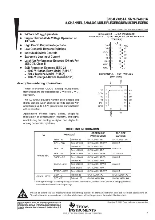
The 74HC/HCT4051 are 8-channel analog multiplexers/demultiplexers with three digital select inputs (S0 to S2), an active LOW enable input (E), eight independent inputs/outputs (Y0 to Y7) and a common input/output (Z).
NAME AND FUNCTION common input/output enable input (active LOW) negative supply voltage ground (0 V) select inputs independent inputs/outputs positive supply voltage
for VI < −0.5 V or VI > VCC + 0.5 V for VS < −0.5 V or VS > VCC + 0.5 V for −0.5 V < VS < VCC + 0.5 V
CONDITIONS
CL = 15 pF; RL = 1 kΩ; VCC = 5 V
TYPICAL
HC
HCT
SYMBOL
PARAMETER
tPZH/ tPZL
tPHZ/ tPLZ
CI CPD CS
turn “ON” time E to Vos Sn to Vos
turn “OFF” time E to Vos Sn to Vos
input capacitance power dissipation capacitance per switch max. switch capacitance
DC switch current
DC VEE current DC VCC or GND current storage temperature range −65
power dissipation per package
+11.0 V 20 mA 20 mA 25 mA 20 mA 50 mA +150 °C
74HC/HCT4051 8-channel analog multiplexer/demultiplexer
Product specification File under Integrated Circuits, IC06
December 1990
元器件交易网
Philips Semiconductors
元器件交易网
INTEGRATED CIRCUITS
DATA SHEET
For a complete data sheet, please also download:
• The IC06 74HC/HCT/HCU/HCMOS Logic Family Specifications • The IC06 74HC/HCT/HCU/HCMOS Logic Package Information • The IC06 74HC/HCT/HCU/HCMOS Logic Package Outlines
Y4 − Z Y5 − Z Y6 − Z Y7 − Z
none
Fig.4 Functional diagram.
December 1990
Fig.5 Schematic diagram (one switch). 4
元器件交易网
Philips Semiconductors
8-channel analog multiplexer/demultiplexer
Product specification
74HC/HCT4051
FEATURES
• Wide analog input voltage range: ± 5 V. • Low “ON” resistance:
80 Ω (typ.) at VCC − VEE = 4.5 V 70 Ω (typ.) at VCC − VEE = 6.0 V 60 Ω (typ.) at VCC − VEE = 9.0 V • Logic level translation: to enable 5 V logic to communicate with ± 5 V analog signals • Typical “break before make” built in • Output capability: non-standard • ICC category: MSI
22
22
20
24
UNIT
ns ns
notes 1 and 2
18
16
ns
19
20
ns
3.5
3.5
pF
25
25
pF
5
5
pF
25
25
pF
Notes
1. CPD is used to determine the dynamic power dissipation (PD in µW): PD = CPD × VCC2 × fi + ∑ { (CL + CS ) × VCC2 × fo } where:
750 mW above +70 °C: derate linearly with 12 mW/K 500 mW above +70 °C: derate linearly with 8 mW/K
PS
power dissipation per switch
100 mW
Note to ratings
1. To avoid drawing VCC current out of terminal Z, when switch current flows in terminals Yn, the voltage drop across the bidirectional switch must not exceed 0.4 V. If the switch current flows into terminal Z, no VCC current will flow out of terminals Yn. In this case there is no limit for the voltage drop across the switch, but the voltages at Yn and Z may not exceed VCC or VEE.
2. For HC the condition is VI = GND to VCC For HCT the condition is VI = GND to VCC − 1.5 V
December 1990
2
元器件交易网
Philips Semiconductors
8-channel analog multiplexer/demultiplexer
8-channel analog multiplexer/demultiplexer
Product specification
74HC/HCT4051
APPLICATIONS
• Analog multiplexing and demultiplexing • Digital multiplexing and demultiplexing • Signal gating
VCC and GND are the supply voltage pins for the digital control inputs (S0 to S2, and E). The VCC to GND ranges are 2.0 to 10.0 V for HC and 4.5 to 5.5 V for HCT. The analog inputs/outputs (Y0 to Y7, and Z) can swing between VCC as a positive limit and VEE as a negative limit. VCC − VEE may not exceed 10.0 V.
SYMBOL
PARAMETER
MIN. MAX. UNIT
CONDITIONS
VCC ±IIK ±ISK ±IS ±IEE ±ICC; ±IGND Tstg Ptot
DC supply voltage
−0.5
DC digital input diode current
DC switch diode current
fi = input frequency in MHz fo = output frequency in MHz ∑ { (CL + CS) × VCC2 × fo } = sum of outputs CL = output load capacitance in pF CS = max. switch capacitance in pF VCC = supply voltage in V
With E LOW, one of the eight switches is selected (low impedance ON-state) by S0 to S2. With E HIGH, all switches are in the high impedance OFF-state, independent of S0 to S2.
independent (Y) common (Z)
“4000B” series. They are specified in compliance with JEDEC standard no. 7A.
The 74HC/HCT4051 are 8-channel analog multiplexers/demultiplexers with three digital select inputs (S0 to S2), an active LOW enable input (E), eight independent inputs/outputs (Y0 to Y7) and a common input/output (Z).
NAME AND FUNCTION common input/output enable input (active LOW) negative supply voltage ground (0 V) select inputs independent inputs/outputs positive supply voltage
for VI < −0.5 V or VI > VCC + 0.5 V for VS < −0.5 V or VS > VCC + 0.5 V for −0.5 V < VS < VCC + 0.5 V