74LVT162240DGGRE4中文资料
- 格式:pdf
- 大小:211.81 KB
- 文档页数:12
SN54LVT162240, SN74LVT1622403.3-V ABT 16-BIT BUFFERS/DRIVERSWITH 3-STATE OUTPUTS SCBS719 – JULY 2000
1POST OFFICE BOX 655303 • DALLAS, TEXAS 75265
DMembers of the Texas Instruments
Widebus™ Family
DState-of-the-Art Advanced BiCMOS
Technology (ABT) Design for 3.3-VOperation and Low Static-PowerDissipationDOutput Ports Have Equivalent 22-Ω Series
Resistors, So No External Resistors AreRequiredDSupport Mixed-Mode Signal Operation
(5-V Input and Output Voltages With3.3-V VCC)
DSupport Unregulated Battery Operation
Down to 2.7 VDTypical V
OLP (Output Ground Bounce)
<0.8 V at VCC = 3.3 V, TA = 25°C
DI
off and Power-Up 3-State Support Hot
InsertionDDistributed V
CC and GND Pins Minimize
High-Speed Switching NoiseDFlow-Through Architecture Optimizes PCB
LayoutDLatch-Up Performance Exceeds 100 mA Per
JESD 78, Class IIDESD Protection Exceeds JESD 22
– 2000-V Human-Body Model (A114-A)– 200-V Machine Model (A115-A)– 1000-V Charged-Device Model (C101)DPackage Options Include Plastic Shrink
Small-Outline (DL), Thin ShrinkSmall-Outline (DGG), and Thin VerySmall-Outline (DGV) Packages and 380-milFine-Pitch Ceramic Flat (WD) PackageUsing 25-mil Center-to-Center Spacings
NOTE:For tape and reel order entry: The DGGR package is abbreviated to GR, andthe DGVR package is abbreviated to VR.
descriptionThe ’LVT162240 devices are 16-bit buffers/drivers designed specifically for low-voltage (3.3-V) VCC operationand to improve both the performance and density of 3-state memory address drivers, clock drivers, andbus-oriented receivers and transmitters. They have the capability to provide a TTL interface to a 5-V systemenvironment.
These devices can be used as four 4-bit buffers, two 8-bit buffers, or one 16-bit buffer and provide invertingoutputs and symmetrical active-low output-enable (OE) inputs.
Copyright © 2000, Texas Instruments IncorporatedUNLESS OTHERWISE NOTED this document contains PRODUCTION
DATA information current as of publication date. Products conform tospecifications per the terms of Texas Instruments standard warranty.Production processing does not necessarily include testing of allparameters.
Please be aware that an important notice concerning availability, standard warranty, and use in critical applications ofTexasInstruments semiconductor products and disclaimers thereto appears at the end of this data sheet.
Widebus is a trademark of Texas Instruments.
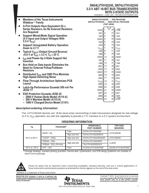
123456789101112131415161718192021222324484746454443424140393837363534333231302928272625
1OE1Y11Y2GND1Y31Y4VCC2Y12Y2GND2Y32Y43Y13Y2GND3Y33Y4VCC4Y14Y2GND4Y34Y44OE2OE1A11A2GND1A31A4VCC
2A1
2A2GND2A32A43A13A2GND3A33A4VCC
4A1
4A2GND4A34A43OE
SN54LVT162240...WD PACKAGESN74LVT162240...DGG, DGV, OR DL PACKAGE(TOP VIEW)
元器件交易网www.cecb2b.comSN54LVT162240, SN74LVT1622403.3-V ABT 16-BIT BUFFERS/DRIVERSWITH 3-STATE OUTPUTS SCBS719 – JULY 2000
2POST OFFICE BOX 655303 • DALLAS, TEXAS 75265
description (continued)The outputs, which are designed to source or sink up to 12 mA, include equivalent 22-Ω series resistors toreduce overshoot and undershoot.
When VCC is between 0 and 1.5 V, the devices are in the high-impedance state during power up or power down.
However, to ensure the high-impedance state above 1.5 V, OE should be tied to VCC through a pullup resistor;the minimum value of the resistor is determined by the current-sinking capability of the driver.
These devices are fully specified for hot-insertion applications using Ioff and power-up 3-state. The Ioff circuitrydisables the outputs, preventing damaging current backflow through the devices when they are powered down.The power-up 3-state circuitry places the outputs in the high-impedance state during power up and power down,which prevents driver conflict.
The SN54LVT162240 is characterized for operation over the full military temperature range of –55°C to 125°C.The SN74LVT162240 is characterized for operation from –40°C to 85°C.
FUNCTION TABLE(each 4-bit buffer/driver)
INPUTSOUTPUT
OEAY
LHLLLHHXZ
元器件交易网www.cecb2b.com