
74ACT16244MTD中文资料
- 格式:pdf
- 大小:72.08 KB
- 文档页数:7
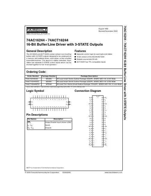

© Semiconductor Components Industries, LLC, 2006June, 2006 − Rev. 51Publication Order Number:
74VCX16244/D74VCX16244
Low−Voltage 1.8V/2.5V/3.3V
16−Bit Buffer
With 3.6 V−Tolerant Inputs and Outputs
(3−State, Non−Inverting)
The 74VCX16244 is an advanced performance, non−inverting16−bit buffer. It is designed for very high−speed, very low−poweroperation in 1.8 V, 2.5 V or 3.3 V systems.When operating at 2.5 V (or 1.8 V) the part is designed to toleratevoltages it may encounter on either inputs or outputs when interfacingto 3.3 V busses. It is guaranteed to be overvoltage tolerant to 3.6 V.
The 74VCX16244 is nibble controlled with each nibble functioningidentically, but independently. The control pins may be tied together toobtain full 16−bit operation. The 3−state outputs are controlled by anOutput Enable (OEn) input for each nibble. When OEn is LOW, theoutputs are on. When OEn is HIGH, the outputs are in the highimpedance state.
74HC14中文资料
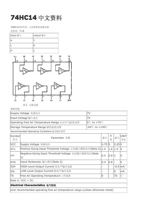
74HC14的作用:六反相斯密特触发器真值表:Y=A
Input输入output输出
AY
LH
HL
图1引脚功能极限参数:SupplyVoltage电源电压7VInputVoltage输入电压7VOperatingFreeAirTemperatureRange自由空气温度范围0℃to+70℃
StorageTemperatureRange储存温度范围-65℃to+150℃RecommendedOperatingConditions建议操作条件Symbol符号Parameter参数最小典型最大UNIT单位
VCCSupplyVoltage电源电压4.7555.25V
VT+Positive-GoingInputThresholdVoltage正向输入阈值电压(Note2)1.41.61.9V
VT-Negative-GoingInputThresholdVoltage反向输入阈值电压(Note2)0.50.81V
HYSInputHysteresis输入滞后(Note2)0.40.8-V
IOHHIGHLevelOutputCurrent高电平输出电流---0.4mA
IOLLOWLevelOutputCurrent低电平输出电流--8mA
TAFreeAirOperatingTemperature工作温度0-70℃
Note2:VCC=5V.
ElectricalCharacteristics电气特性
overrecommendedoperatingfreeairtemperaturerange(unlessotherwisenoted)Symbol符号Parameter参数Conditions条件最小典型最大UNIT单位
VIInputClampVoltage输入钳位电压VCC=最小,II=-18mA---1.5V
VOHHIGHLevelOutputVoltage输出高电平电压VCC=最小,IOH=最大VIL=最大2.73.4-V

AC244中文资料
MC74AC244, MC74ACT244Octal Buffer/Line Driver with 3-State Outputs
The MC74AC244/74ACT244 is an octal buffer and line driver
designed to be employed as a memory address driver, clock
driver and bus oriented transmitter/receiver which provides
improved PC board density.
3–State Outputs Drive Bus Lines or Buffer Memory Address
Registers
Outputs Source/Sink 24 mA
′ACT244 Has TTL Compatible Inputs
V OE OE 1
GND
Figure 1. Pinout: 20–Lead Packages Conductors (Top View)
NOTE:
H = HIGH Voltage Level L = LOW Voltage Level X =
Immaterial
Z = High Impedance
NOTE:
H = HIGH Voltage Level L = LOW Voltage Level X =
Immaterial
Z = High Impedance
1
PDIP–20N SUFFIX
CASE 738
1
1 1 SO–20DW SUFFIX CASE 751
TSSOP–20DT SUFFIX CASE 948E EIAJ–20M SUFFIX CASE 967
Device
Package Shipping ORDERING INFORMATION
MC74AC244N PDIP–2018 Units/Rail MC74ACT244N PDIP–2018 Units/Rail MC74AC244DW SOIC–2038 Units/Rail

74LVT2244
33V
ABT
Octal
BufferLine
Driver
with
TRI-STATE
Outputs
ADVANCEINFORMATION
December1996
74LVT2244
33VABTOctalBufferLineDriver
withTRI-STATEOutputs
GeneralDescription
TheLVT2244isanoctalbufferandlinedriverdesignedto
beemployedasamemoryaddressdriverclockdriverand
busorientedtransmitterorreceiverwhichprovidesim-
provedPCboarddensityTheequivalent25X-Seriesresis-
torhelpsreduceoutputovershootandundershoot
Theseoctalbuffersandlinedriversaredesignedforlow-
voltage(33V)VCCapplicationsbutwiththecapabilityto
provideaTTLinterfacetoa5VenvironmentTheLVT2244
isfabricatedwithanadvancedBiCMOStechnologyto
achievehighspeedoperationsimilarto5VABTwhilemain-
tainingalowpowerdissipationFeatures
YInputandoutputinterfacecapabilitytosystemsat5V
VCC
YBus-Holddatainputseliminatetheneedforexternal
pull-upresistorstoholdunusedinputs