
FXA9079-Wafer_unload_system_for_Rena_Texture
- 格式:pdf
- 大小:2.99 MB
- 文档页数:48

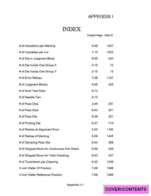
APPENDIX I INDEXChapter-PageData ID# of Actuations per Marking5-061407# of Cassettes per Lot7-101522# of Die in Judgment Block6-05244# of Die Inside One Group X2-1012# of Die Inside One Group Y2-1013# of Error Retries7-061107# of Judgment Blocks6-05245# of Multi Test Sites9-13# of Needle Tips9-13# of Pass Dice2-04251# of Pass Dice6-03251# of Pass Die6-28251# of Probing Die6-27710# of Retries at Alignment Error3-031192# of Retries of Marking5-091445# of Sampling Pass Die6-04258# of Skipped Rows for Continuous Fail Check6-09226# of Skipped Rows for Yield Checking6-03247# of Touchdown per Cleaning6-2213394 inch Wafer ID Position 7-0910864 inch Wafer Reference Position 7-091085Appendix I-1COVER/CONTENTS4.5 inch Wafer ID Position 7-0910884.5 inch Wafer Reference Position 7-0910875 inch Wafer ID Position 7-0910905 inch Wafer Reference Position 7-0910896 inch Wafer ID Position 7-0910926 inch Wafer Reference Position 7-0910918 inch Cassette Specification?7-0210098 inch Wafer ID Position 7-0910948 inch Wafer Reference Position 7-091093AA-PM-6000A Compatible Mode8-072047Adaptive Device - n9-14Adding Basic Operation Data When dd, du8-072455Agreement Device Data Settings9-14Alarm Auto Off Time9-092120Alignment Lighting/Brightness Settings3-05Alignment Main Axis3-0341Alignment Mode3-0448Alignment Range3-0443Alignment Start Position X3-0444Alignment Start Position Y3-0445All Lot Finish Signal (EC)8-081965Amount of Chuck Movement on X axis WhenNeedle Cleaning at Contact Height6-231375Amount of Chuck Movement on Y axis WhenNeedle Cleaning at Contact Height6-231376Appointment CAT. Yield Check Settings6-07Appendix I-2Appointment of Drive Marker by Category5-061414Assot. Of Auto Needle Height Setting3-191238Auto Pad Selection Margin6-15293BBIN Count Check for DUT of Execute Mode6-06268BIN Count Check for DUT Setting6-06Block Size for Block Sampling X4-05165Block Size for Block Sampling Y4-05166Brightness 6-15291Brightness for Wafer ID Reading7-071153Brightness Setting6-15295Brush Needle Cleaning Sequence Settings6-25Brush Needle Cleaning Settings6-25Bump Height (Standard: 0)2-0764CCalculate Checksum?7-061102Calculation of Broken Wafer Center2-071184Calculation of Measurement Position of Broken Wa2-081185Card Name9-15Card Preheat Time3-201227Card Type9-12Cassette # of Characters7-111534Cassette Spec. for 4, 5 & 6 inch WF.7-021007Category # for Repeat Touchdown8-041996Category Check Settings4-13Category Data for Multi Pass Probing4-14Appendix I-3Category Limit Setting6-07Category Numbered?9-102108Center Area Extent3-24213Change for contact height by Z-SW at stop of prob4-111262Character Settings7-08Check BIN No.6-06270Check Category Settings6-11Check Category Settings6-12Check Lot # of Characters7-111528Check of Marker Adjustment5-051418Check Time8-04Check Timing of Marker Actuation Limit5-051416Chuck Center Offset3-24216Chuck height revise function changed chuck tempe3-222189Chuck Position after Lot End7-031017Chuck Temperature (deg)2-0333Cleaning Area Margin from Wafer Edge6-242283Cleaning Contact Interval6-221359Cleaning Count for Contact Count Wafer Cleaning6-242288Cleaning Overdrive6-221338Cleaning Touchdown Limit (Cleaning Limit)6-231341Cleaning Unit6-221332Cleaning Unit Height6-221335Cleaning Wafer Flat/Notch Direction6-241373Cleaning Wafer Flat/Notch Setting6-241346Cleaning Wafer Size6-241333Appendix I-4Cleaning Wafer Thickness6-241334Clear Lot # at Lot End?7-101545Clearance4-101263Color of Wafer ID Characters7-061101Combination of Wafer Management ID7-101523Command Complete Signal (MC) Settings8-08Confirm of Auto Needle Height Adjustment3-191231Cont. Fail Mark NG Limit5-091438Contact Check Method3-171253Contact Count9-15Contact Count in Wafer2-04218Contact Die in No Protrude Probing4-122213Contact Position Control of Probe Card4-121268Continuous Fail between Chip Settings6-12Continuous Fail between Chip?6-121276Continuous Fail Tolerant Die #6-14289Coordinate Origin3-161246Copy Data changing location?9-112183Correlation Continual Failcheck Settings6-28Correlation Load from6-27704Correlation Map Settings6-28Correlation Probing Mode6-27706Correlation Yield Check Settings6-28DData ID Display?9-092111DATA IN at Sampling Start Die?3-171243Appendix I-5DATA IN at Sampling Start Die?4-051243Default Operation Unit9-092109Delay after Marker Actuation5-051404Delay after Reaching Temperature2-0337Delay Time before PIN Up7-031018Delay Time on Subchuck7-031019Device2-021Device Attribute Display?9-102107Device Data Store after Map Change by Sequence9-102148Device for Outputting Results5-091459Device for Outputting Results6-161314Device List Data Display?9-102113Dice for Multi Pass Probing4-141381Die Gross6-03252Die Gross6-28273Die Interval for Brush Cleaning6-251351Die Interval for Cleaning6-221336Die Interval of Fail Mark Inspection5-081440Die Interval of Needle Inspection6-151292Direction of Probing Start4-101261Display # of Remaining Wafers?9-081954Display Center Coordinates?6-171305Display Chuck Height?9-081953Display Coordinates?9-081952Display Fail Mark Diameter?5-111451Display Fail Mark Size?5-111450Appendix I-6

EV Group Europe & Asia/Pacific GmbHDI Erich Thallner Strasse 14782 St. Florian am InnAustria+43 7712 5311 0Contact*******************Printed on paper from sustainable sources. Data, design and specifications may not simultaneously apply
;
o
r
depend on individual equipment configuration, process conditions and materials and may vary accordingly. EVG reserves the
right to change data, design and specifications without prior notice. All trademarks, logos, website addresses or equipment names are registered trademarks and/or the property of EV Group or their respective owners.
© EV Group (EVG). All rights reserved. V22/01Features ■Advanced Alignment Capabilities - Live alignment <± 300 nm (process dependent) ■UV LED lamp up to high power 500 mW/cm² - > 90 % uniformity - Optional: Dual wavelength operation: 365 nm and 405 nm - Different exposure modes ■Optional Features - Optical wedge error compensation (WEC) - Temperature-controlled chuck ■Industry leading process performance - Resolution down to single nanometer range - Very precise residual layer controlIntroductionMultifunctional UV Nanoimprint Lithography system up to 300 mm featuring SmartNIL® technology, lens molding and lens stacking in one tool The versatile EVG7300 UV Nanoimprint Lithography System can support multiple related UV processes: SmartNIL, Wafer Level Optics (WLO) and Stacking – three capabilities merged in one flexible tool.It is a standalone system based on the modularized and improved SmartNIL module, which can be configured depending on handling and automation levels. Supporting wafer sizes from 150 mm up to 300 mm and featuring high-precision alignment down to 300 nm, advanced process control and high throughput, the EVG7300 can serve advanced R&D up to high-volume manufacturing (HVM) needs for a variety of freeform and high precision nano- and micro optical components and devices. For the necessity of integrated pre- and post-process flows in HVM environments, the module can be integrated into the HERCULES NIL system. This multi-functional system is designed to serve a wide range of emerging applications involving micro- and nanoimprints as wel as UV-stacking of functional layers. Thus, the equipment enables enhanced process performance for wafer-level optics (WLO), nanophotonics, metasurfaces and biomedical chips. This is closely related to the industry needs for novel optical sensors and optoelectronics to enable e.g. autonomous driving, micro lens arrays and projectors in automotive and decorative lighting, diffractive optics for biometric authentication as well as emerging trends for sophisticated meta-lenses. First applications utilizing this technology already exist today in the field of advanced biomedical devices and augmented reality waveguides where nanoimprinting enables high quality manufacturing of complex designs.EVG®7300UV Nanoimprint Lithography System
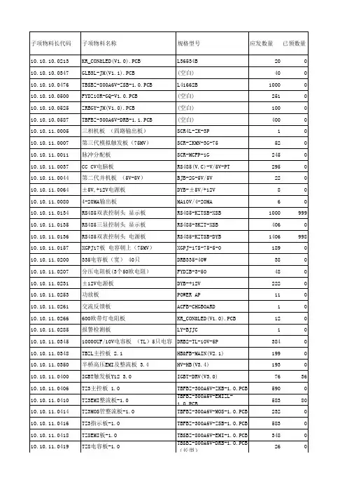
子项物料长代码子项物料名称规格型号应发数量已领数量10.10.10.0213KR_CON&LED(V1.0).PCBL36534B20010.10.10.0347GLB3L-JH(V1.1).PCB(空白)40010.10.10.0476TBSBZ-800A6V-ZSB-1.0.PCBL41662B1000010.10.10.0500FYDZ10R-GQ-V1.0.PCB(空白)251010.10.10.0525ZRBGY-JH(V1.0).PCB(空白)100010.10.10.0587TBFBZ-300A6V-DRB-1.1.PCB(空白)400010.10.11.0005三相机板 (四路输出板)SCR4L-ZK-3P1010.10.11.0007第三代模拟触发板(75MV)SCR-ZKMN-3G-7552010.10.11.0011脉冲分配板SCR-MCFP-1G245010.10.11.0037CC CV电脑板RS485(V.C)-V/5V-PT295010.10.11.0044第二代并机板 (5V-5V)BJB-2G-5V/5V22010.10.11.0064±5V,+12V电源板DYB-±5V/+12V8010.10.11.00804-20MA输出板MA10V/4-20MA6010.10.11.0134RS485双表控制头 显示板RS485-KZTSB-XSB100099910.10.11.0135RS485三显控制头 显示板RS485-3KZT-XSB406010.10.11.0136RS485双表控制头 电源板RS485-KZTSB-DYB140699810.10.11.0157XGPJ17板 电容朝上(75MV)XGPJ-17S-75-5-0189010.10.11.0200335电容板(宽) 40只DRB335-40W38010.10.11.0207分压电阻板(3个50欧电阻)FYDZB-3-5048010.10.11.0231±12V电源板DYB-+12V222010.10.11.0253功放板POWER AP11010.10.11.0261交流反馈板ACFB-CHGBOARD1010.10.11.0266600欧带灯电阻板KR_CON&LED(V1.0).PCB12010.10.11.0285报警检测板LY-BJJC1010.10.11.034510000UF/10V电容板 (TL)5只电容DRB2-TL-10V-5P384010.10.11.0348TBZL主控板 2.1HB&FB-MAIN(V2.1)199010.10.11.0350半桥高压EMI及整流板 3.4HV-HB(V3.4)193010.10.11.0400IGBT触发板Y12 3.0IGBT-DRV(V3.0)763610.10.11.0406TZ3主控板 1.0TBFBZ-300A6V-ZKB-1.0.PCB590010.10.11.0410TZ3EMI整流板-1.0TBFBZ-300A6V-EMIZL-1.0.PCB5838010.10.11.0414TZ3MOS管整流板-1.0TBFBZ-300A6V-MOS-1.0.PCB232010.10.11.0416TZ3指示板-1.0TBFBZ-300A6V-ZSB-1.0.PCB583010.10.11.0418TZ8EMI板-1.0TBSBZ-800A6V-EMI-1.0.PCB348010.10.11.0419TZ8电容板-1.0TBSBZ-800A6V-DRB-1.0.PCB(长26010.10.11.0421TZ8指示板-1.0TBSBZ-800A6V-ZSB-1.0.PCB332010.10.11.0422TZ8MOS管整流板-1.0TBSBZ-800A6V-MOS-1.0.PCB2726410.10.11.0425分压电阻板(10个100欧电阻)1.0FYDZ10R-GQ-V1.01152010.10.11.0428正负脉冲机底板 4.0正负脉冲机底板(4.0).PCB39010.10.11.0429正负脉冲机通讯板 4.0正负脉冲机通讯板(V4.0).PCB156010.10.11.0447TZ8电容板2-1.0-1(风冷)TBFBZ-800A6V-DRB2-1.0.PCB26010.10.11.0448TZ8指示板-1.0-1TBFBZ-800A6V-ZSB-1.0.PCB48010.10.11.0469TZ3KIGBT辅助板1.0TBSBZ-3000A7V-IGBTFZ-1.0-PC241215610.10.11.0478TZ3驱动板-1.1TBFBZ-300A6V-QDB-1.1.PCB485010.10.11.0479TZ8驱动板-1.1TBFBZ-300A6V-QDB-1.1.PCB348010.10.11.0480TZ3同步驱动板-1.1TBFBZ-300A6V-TBQD-1.1.PCB485010.10.11.0501TZL300IGBT板1.0TBSBZ-2500A15V-IGBT-1.0-PCB82510010.10.11.0502TZL300IGBT辅助板1.2TBSBZ-2500A15V-IGBTFZ-1.2-P164120010.10.11.0506TZ3电容板-1.1TBFBZ-300A6V-DRB-1.1.PCB62910610.10.11.0511TZ3KIGBT板1.1TBSBZ-3000A7V-IGBT-1.1-PCB12077810.10.11.0519TZ3KEMI整流板1.1TBSBZ-3000A7V-EMIZL-1.1-PCB3787810.10.11.0522TZL300EMI整流板1.0TBSBZ-2500A15V-EMIZL-1.0-PC82610010.10.11.0529TZ2KEMI板1.0TBSBZ-2000A7V-EMI-1.0-PCB812010.10.11.0530TZ3K电源板1.0TBFBZ-3000A12V-DYB-1.01083.115010.10.11.0531TZ3KMOS管板1.1TBFBZ-3000A12V-MOS-1.145892010.10.11.0534双输出并机通讯板2.1AConvert2-A-HB-Ver2.1164010.10.11.0535双输出并机通讯板2.1BConvert2-B-HB-Ver2.1164010.10.11.0536ZY通讯板1.0TXB-ZY(1.0)-PCB296417810.10.11.0546TZ光耦隔离板 1.3GOGL-ZY(V1.3).PCB4-1810.10.11.0548LM2575DC模块板LM2575-DC-DC-ZXY-Ver1.0164010.10.11.0551TZ一体化表头DispBoard-HB-Ver1.016010.10.11.0555TZ3逆变板-1.1TBFBZ-300A6V-NB-1.1-PCB485010.10.11.0556TZ8主电路板-1.1TBSBZ-800A6V-ZDL-1.1-PCB348010.10.11.0558TZL150电源驱动板1.3TBSBZ-3000A7V-DYQD-1.3-PCB12057810.10.11.0562TZF1.2KEMI板TBFBZ-1200A12V-EMI-1.0-PCB16010.10.11.0563TZ8电容板-1.1TBSBZ-800A6V-DRB-1.1.PCB(正322010.10.11.0565TZ主控扩展板1.1TBFBZ-300A6V-ZKB-EXT-PCB1.118010.10.11.0566TZ直插调宽小板 1.0TBFBZ-300A6V-CW-EXT-PCB1.0(18010.10.11.0577TZ温度板-1.1TBFBZ-300A6V-WDB-1.1.PCB833010.10.11.058924脉波可控硅整流模拟控制板1.3SCR-ANALOG-HB-VER1.311010.10.11.0591三路隔离板(电压型)GLB3L-JH(V1.1)10010.10.11.0604TZF8整流板1.0TBFBZ-800A12V-ZLB-1.0.PCB14010.10.11.060816路PT100温度采集板 1.0PT100-16-HB-VER1.0.PCB 4层 40010.10.11.0613TZ6换向驱动板 1.0TBFBZ-600A15V-HXQDB-1.0.PCB15010.10.11.0615TZ50A主电路板1.1TBFBZ-50A6V-ZDL-1.1.PCB 2层16010.10.11.0617TZ50A主控板1.1TBFBZ-50A6V-ZKB-1.1.PCB 4层16010.11.13.0018金属膜电阻 1WRJ16-1W-1KΩ-±1%20010.11.13.0053碳膜电阻 1WRJ16-1W-2KΩ-±1%20010.11.14.0028金属膜电阻 2WRJ17-2W-150Ω-±1%3010.11.14.0029金属膜电阻 2WRJ17-2W-300Ω-±1%3010.11.14.0031金属膜电阻 2WRJ17-2W-600Ω-±1%123010.11.14.0032金属膜电阻 2WRJ17-2W-1.2KΩ-±1%3010.11.14.0063合金电阻 2512 2WMLF12MR004FT 0.004Ω±1%(2W)100010.11.15.0007碳膜电阻 5WRT29-5W-100Ω-±5%451042810.11.20.0010压敏电阻 MYN5-350V-5KJMYN5-350V-±10%12010.11.21.0003金属电阻 50WRX12-50W-150Ω-±5﹪500010.11.22.0014水泥电阻 50WRN12-50W-50Ω-±5﹪227515010.11.25.0003绕线电阻RX21-6W-47Ω-±1%647010.12.11.0156薄膜电容 DGT 1UF 500V.AC ±5%(空白)48010.12.12.0156贴片电容 0805 224 0.22UF 25V 10% 08(空白)40010.13.10.0071发光二极管红发红光-(1.8-2.4V)/20mA-圆Φ3 无边灯 插装3000010.13.10.0072发光二极管绿发绿光-(1.8-2.4V)/20mA-圆Φ3 无边灯 插装6000010.20.00.0010指示灯APT-AD16-22D/y31S AC220V 黄Ф22 上海二工206010.20.00.0012指示灯APT-AD16-22D/g23S DC24V 绿色Ф22 上海二工410010.21.00.0003蜂鸣器APT-AD16-22SM/R23 DC24V Φ22 红色 上海二工399010.22.00.0002警示灯安装底座TL-SZ-12010.22.00.0007接线座TL-70L 上海二工2010.22.00.0008装饰盖TL-70C 上海二工2010.22.00.0014声组件TL-70BI/31 APT2010.22.00.0015光组件TL-70LS/y31 APT2010.22.00.0016光组件TL-70LS/g31 APT2010.22.00.0017光组件TL-70LS/r31 APT2010.23.00.0020发光二极管座3MM-3三孔座(15.24*4.32*11.Ф=3mm)3000010.24.00.0018MOS管IRFS3004-7PPBF 240A40V 贴片192010.24.00.0034MOS管IRFS3004TRL7PP 195A40V 贴片919361920010.25.12.0028模块型整流管MBRP300200CT 300A200V 模块型286010.25.12.0036模块型整流管MURP30060CT 300A600V 模块型4846

Arria II Device Architecture
■Diagnostic features
■Serial loopback from the transmitter serializer to the receiver CDR for
transceiver physical coding sublayer (PCS) and PMA diagnostics
■Parallel loopback from the transmitter PCS to the receiver PCS with built-in self
test (BIST) pattern generator and verifier
■Reverse serial loopback pre- and post-CDR to transmitter buffer for physical
link diagnostics
■Loopback master and slave capability in PCIe hard IP blocks
■Support for protocol features such as MSB-to-LSB transmission in a
SONET/SDH configuration and spread-spectrum clocking in a PCIe
configuration
Table1–5 lists common protocols and the ArriaII dedicated circuitry and features for
implementing these protocols.
1For other protocols supported by ArriaII devices, such as SONET/SDH, SDI, SATA
and SRIO, refer to the Transceiver Architecture in Arria II Devices chapter.Table1–5.Sample of Supported Protocols and Feature Descriptions for Arria II DevicesSupported ProtocolsFeature Descriptions