LV2283VB中文资料
- 格式:pdf
- 大小:123.82 KB
- 文档页数:10
SpecificationsofanyandallSANYOSemiconductorCo.,Ltd.productsdescribedorcontainedhereinstipulatetheperformance,characteristics,andfunctionsofthedescribedproductsintheindependentstate,andarenotguaranteesoftheperformance,characteristics,andfunctionsofthedescribedproductsasmountedinthecustomer'sproductsorequipment.Toverifysymptomsandstatesthatcannotbeevaluatedinanindependentdevice,thecustomershouldalwaysevaluateandtestdevicesmountedinthecustomer'sproductsorequipment.AnyandallSANYOSemiconductorCo.,Ltd.productsdescribedorcontainedhereinare,withregardto"standardapplication",intendedfortheuseasgeneralelectronicsequipment(homeappliances,AVequipment,communicationdevice,officeequipment,industrialequipmentetc.).Theproductsmentionedhereinshallnotbeintendedforuseforany"specialapplication"(medicalequipmentwhosepurposeistosustainlife,aerospaceinstrument,nuclearcontroldevice,burningappliances,transportationmachine,trafficsignalsystem,safetyequipmentetc.)thatshallrequireextremelyhighlevelofreliabilityandcandirectlythreatenhumanlivesincaseoffailureormalfunctionoftheproductormaycauseharmtohumanbodies,norshalltheygrantanyguaranteethereof.Ifyoushouldintendtouseourproductsforapplicationsoutsidethestandardapplicationsofourcustomerwhoisconsideringsuchuseand/oroutsidethescopeofourintendedstandardapplications,pleaseconsultwithuspriortotheintendeduse.Ifthereisnoconsultationorinquirybeforetheintendeduse,ourcustomershallbesolelyresponsiblefortheuse.
D2607 MS 20071211-S00002 / D1207 MS PC No.A0974-1/10 LV2283VB
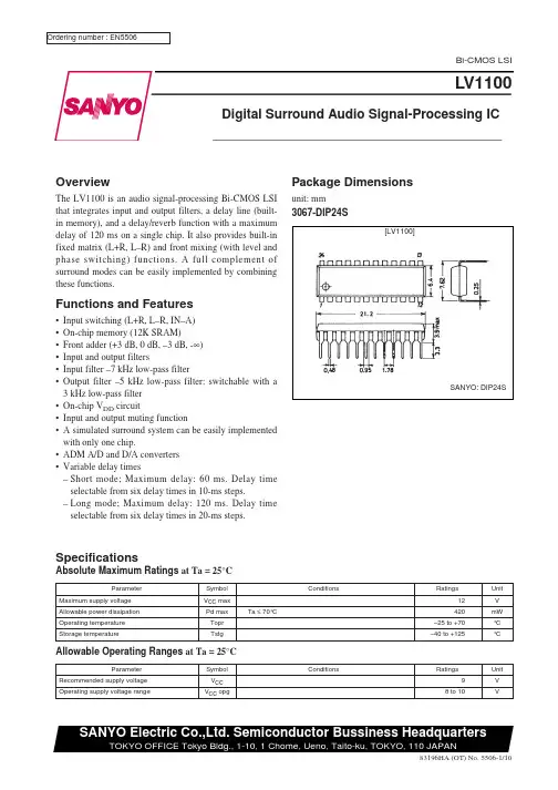
Overview The LV2283VB is an FM Transmitter IC. MPX block makes stereo modulated, composite signal from L and R sound inputs. RF VCO includes FM modulation function. PLL synthesizer determines RF output frequency with I2C control. Application • Portable Memory Player • Portable HDD Player • Wireless Headphone Features • (Audio) Pilot tone system stereo modulation, audio attenuation • (RF) VCO, programmable gain driver amplifier • (PLL) 70 to 110MHz 100kHz step • (Bus control) I2C bus control • (Regulator) 2.8V LDO regulator Specifications Absolute Maximum Ratings at Ta = 25°C Parameter Symbol Conditions Ratings
Unit Maximum supply voltage VCC max Pin 6 7.0V Maximum input voltage VIN max VCC+0.3V Minimum input voltage VIN min -0.3V Allowable power dissipation Pd max Ta ≤ 85°C, Mounted on a specified board* 500mW Operating temperature Topr -40 to +85°C Storage temperature Tstg -55 to +150°C * Specified board : 114.3mm×76.1mm×1.6mm, glass epoxy circuit board. Bi-CMOSICFM Transmitter IC with
Stereo ModulationOrdering number : ENA0974A 元器件交易网www.cecb2b.comLV2283VB No.A0974-2/10 Recommended Operating Conditions at Ta = 25°C Parameter Symbol Conditions Ratings Unit Recommended supply voltage VCC Pin 6 3.3 V Operating supply voltage range VCC op Pin 6 2.8 to 5.5 V AC Characteristics Ta = 25°C, VCC = 3.3V, I2C bits = Default state, L and R input = 1kHz, 450mVrms, unless otherwise noted Ratings Parameter Symbol Conditions min typ max Unit Circuit current ICC No input signal, Pin 6 current 8 10 mA Standby current ISTB No input signal, I2C bit “STB” = “1”, Pin 6 current 1.0 µA
Audio and MPX Blocks Ratings Parameter Symbol Conditions min typ max Unit Maximum audio input VA max Pin 1 and 24 input 900 mVrms Audio input frequency FAF Pin 1 and 24 input 20 15k Hz Channel separation SEP Pin 7, composite output, L→R, R→L 2035 dB Channel balance CB Pin 7, composite output -20 2 dB Total harmonic distortion THD Pin 7, composite output 0.1 0.3 % Pilot tone output level PMOD I2C bits “ST” =”1” 0.50.85 1.2 mVp-p Composite output level MPXOUT 3.33.8 4.3 mVrms Audio mute MUTE I2C bit “MUTE” = “1” 3035 dB Audio attenuation adjustment step ATTSTEP I2C bit “ATT2 – ATT0” = “000” to “111”, totally 8 steps. 1.52 2.5 dB
Crystal oscillator frequency (1) FXOSC (1) Pin 21 and Pin 22 76 kHz RF Blocks Ratings Parameter Symbol Conditions min typ max Unit RF output RFOUT f = 98MHz, I2C bit “RF2 - RF0” = “011”, Pin 12 output 109112 115 dBµV
RF output adjustment step RFSTEP I2C bit “RF2 – RF0” = “000” to “111”, totally 8 steps. Pin 12 relative output. 0.40.9 1.4 dB
RF frequency FRF 100kHz step 70 110 MHz PLL Blocks Ratings Parameter Symbol Conditions min typ max Unit I2C input “High” voltage VH 0.8VCC VCC+0.3 V I2C input “Low” voltage VL -0.3 0.2VCC V 19kHz output voltage V19K Pin 20. 19kHz output. I2C bit “19K” = “1”.Load impedance = 47kΩ. 0.6VCC0.8VCC Vp-p
RF input frequency FPLL Step = 100kHz, See table 1 70 110 MHz Crystal oscillator frequency (2) FXOSC (2) Pin 16 16 MHz External clock frequency FEXT External clock injection to Pin 13 instead of 16MHz crystal oscillation. When the LSI is standby mode, external clock should be stop. 1 24 MHz