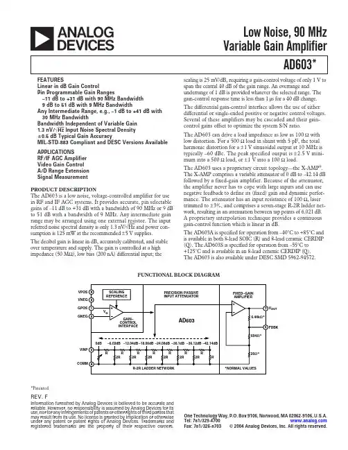
aAD603*FEATURESLinear in dB Gain ControlPin Programmable Gain Ranges–11 dB to +31 dB with 90 MHz Bandwidth 9 dB to 51 dB with 9 MHz BandwidthAny Intermediate Range, e.g., –1 dB to +41 dB with 30 MHz BandwidthBandwidth Independent of Variable Gain 1.3 nV/√Hz Input Noise Spectral Density ؎0.5 dB Typical Gain AccuracyMIL-STD-883 Compliant and DESC Versions Available APPLICATIONSRF/IF AGC Amplifier Video Gain Control A/D Range Extension Signal Measurement Low Noise, 90MHz Variable Gain AmplifierPRODUCT DESCRIPTIONThe AD603 is a low noise, voltage-controlled amplifier for use in RF and IF AGC systems. It provides accurate, pin selectable gains of –11dB to +31dB with a bandwidth of 90 MHz or 9dB to 51 dB with a bandwidth of 9 MHz. Any intermediate gain range may be arranged using one external resistor. The input referred noise spectral density is only 1.3nV/√Hz and power con-sumption is 125 mW at the recommended ±5 V supplies.The decibel gain is linear in dB, accurately calibrated, and stable over temperature and supply. The gain is controlled at a high impedance (50 M Ω), low bias (200 nA) differential input; theFUNCTIONAL BLOCK DIAGRAMOUTscaling is 25 mV/dB, requiring a gain-control voltage of only 1 V to span the central 40 dB of the gain range. An overrange andunderrange of 1 dB is provided whatever the selected range. The gain-control response time is less than 1µs for a 40 dB change.The differential gain-control interface allows the use of either differential or single-ended positive or negative control voltages.Several of these amplifiers may be cascaded and their gain-control gains offset to optimize the system S/N ratio.The AD603 can drive a load impedance as low as 100 Ω with low distortion. For a 500 Ω load in shunt with 5 pF, the total harmonic distortion for a ±1V sinusoidal output at 10 MHz is typically –60 dBc. The peak specified output is ±2.5 V mini-mum into a 500Ω load, or ±1 V into a 100 Ω load.The AD603 uses a proprietary circuit topology—the X-AMP ®.The X-AMP comprises a variable attenuator of 0 dB to –42.14dB followed by a fixed-gain amplifier. Because of the attenuator,the amplifier never has to cope with large inputs and can use negative feedback to define its (fixed) gain and dynamic perfor-mance. The attenuator has an input resistance of 100 Ω, laser trimmed to ±3%, and comprises a seven-stage R-2R ladder net-work, resulting in an attenuation between tap points of 6.021dB.A proprietary interpolation technique provides a continuous gain-control function which is linear in dB.The AD603A is specified for operation from –40°C to +85°C and is available in both 8-lead SOIC (R) and 8-lead ceramic CERDIP (Q). The AD603S is specified for operation from –55°C to +125°C and is available in an 8-lead ceramic CERDIP (Q).The AD603 is also available under DESC SMD 5962-94572.*Patented.REV.FInformation furnished by Analog Devices is believed to be accurate and reliable. However, no responsibility is assumed by Analog Devices for its use, nor for any infringements of patents or other rights of third parties that may result from its use. No license is granted by implication or otherwise under any patent or patent rights of Analog Devices. Trademarks and registered trademarks are the property of their respective owners.One Technology Way, P.O. Box 9106, Norwood, MA 02062-9106, U.S.A.Tel: 781/329-4700 Fax: 781/326-8703© 2004 Analog Devices, Inc. All rights reserved.AD603–SPECIFICATIONSREV. F–2–ModelAD603ParameterConditions Min Typ Max Unit INPUT CHARACTERISTICS Input Resistance Pins 3 to 497100103ΩInput Capacitance2pFInput Noise Spectral Density 1Input Short Circuited1.3nV/√Hz Noise Figuref = 10 MHz, Gain = max, R S = 10 Ω8.8dB 1 dB Compression Point f = 10 MHz, Gain = max, R S = 10 Ω–11dBm Peak Input Voltage±1.4±2V OUTPUT CHARACTERISTICS –3 dB Bandwidth V OUT = 100 mV rms 90MHz Slew Rate R L ≥ 500 Ω275V/µs Peak Output 2R L ≥ 500 Ω±2.5±3.0V Output Impedancef ≤ 10 MHz2ΩOutput Short-Circuit Current 50mA Group Delay Change vs. Gainf = 3 MHz; Full Gain Range ±2ns Group Delay Change vs. Frequency V G = 0 V; f = 1 MHz to 10 MHz ±2ns Differential Gain 0.2%Differential Phase0.2Degree Total Harmonic Distortion f = 10 MHz, V OUT = 1V rms–60dBc Third Order Intercept f = 40 MHz, Gain = max, R S = 50 Ω15dBm ACCURACY f = 10.7 MHzGain Accuracy –500 mV ≤ V G ≤ +500 mV –1±0.5؉1dB T MIN to T MAX–1.5ϩ1.5dB Output Offset Voltage 3V G = 0V–20؉20mV T MIN to T MAX–30ϩ30mV Output Offset Variation vs. V G –500 mV ≤ V G ≤ +500 mV–20؉20mV T MIN to T MAX –30ϩ30mV GAIN CONTROL INTERFACE Gain Scaling Factor 39.44040.6dB/V T MIN to T MAX3842dB/V GNEG, GPOS Voltage Range 4–1.2+2.0V Input Bias Current 200nA Input Offset Current10nA Differential Input Resistance Pins 1 to 250M ΩResponse RateFull 40 dB Gain Change40dB/µs POWER SUPPLYSpecified Operating Range ±4.75±6.3V Quiescent Current 12.517mA T MIN to T MAX20mANOTES 1Typical open or short-circuited input; noise is lower when system is set to maximum gain and input is short-circuited. This figure includes the effects of both voltage and current noise sources.2Using resistive loads of 500Ω or greater, or with the addition of a 1 k Ω pull-down resistor when driving lower loads.3The dc gain of the main amplifier in the AD603 is ×35.7; thus, an input offset of 100 µV becomes a 3.57 mV output offset.4GNEG and GPOS, gain control, and voltage range are guaranteed to be within the range of –V S + 4.2 V to +V S – 3.4 V over the full temperature range of –40°C to +85°C.Specifications shown in boldface are tested on all production units at final electrical test. Results from those tests are used to calculate outgoing quality levels. All min and max specifications are guaranteed, although only those shown in boldface are tested on all production units.Specifications subject to change without notice.(@ T A = 25؇C, V S = ؎5 V, –500 mV ≤ V G ≤ +500 mV, GNEG = 0 V, –10 dB to +30dB Gain Range, R L = 500⍀, and C L = 5 pF, unless otherwise noted.)AD603–3–REV.FABSOLUTE MAXIMUM RATINGS 1Supply Voltage ±V S . . . . . . . . . . . . . . . . . . . . . . . . . . . .±7.5V Internal Voltage VINP (Pin 3) . . . . . . . . . . . ±2 V Continuous . . . . . . . . . . . . . . . . . . . . . . . . . . . . . . . . . . . . ±V S for 10 ms GPOS, GNEG (Pins 1, 2) . . . . . . . . . . . . . . . . . . . . . . . ±V S Internal Power Dissipation 2 . . . . . . . . . . . . . . . . . . . . 400mW Operating Temperature RangeAD603A . . . . . . . . . . . . . . . . . . . . . . . . . . . –40°C to +85°C AD603S . . . . . . . . . . . . . . . . . . . . . . . . . . –55°C to +125°C Storage Temperature Range . . . . . . . . . . . . –65°C to +150°C Lead Temperature Range (Soldering 60sec) . . . . . . . . .300°CNOTES 1Stresses above those listed under Absolute Maximum Ratings may cause perma-nent damage to the device. This is a stress rating only; functional operation of the device at these or any other conditions above those indicated in the operational section of this specification is not implied. Exposure to absolute maximum rating conditions for extended periods may affect device reliability.2Thermal Characteristics:8-Lead SOIC Package: θJA = 155°C/W, θJC = 33°C/W 8-Lead CERDIP Package: θJA = 140°C/W, θJC = 15°C/WPIN FUNCTION DESCRIPTIONSPin No.Mnemonic Description1GPOS Gain-Control Input High(Positive Voltage Increases Gain)2GNEG Gain-Control Input Low(Negative Voltage Increases Gain)3VINP Amplifier Input 4COMM Amplifier Ground5FDBK Connection to Feedback Network 6VNEG Negative Supply Input 7VOUT Amplifier Output 8VPOSPositive Supply InputCONNECTION DIAGRAM 8-Lead Plastic SOIC (R) Package 8-Lead Ceramic CERDIP (Q) PackageVPOSVOUT VNEGFDBKCAUTIONESD (electrostatic discharge) sensitive device. Electrostatic charges as high as 4000V readily accumulate on the human body and test equipment and can discharge without detection. Although the AD603 features proprietary ESD protection circuitry, permanent damage may occur on devices subjected to high energy electrostatic discharges. Therefore, proper ESD precautions are recom-mended to avoid performance degradation or loss of functionality.ORDERING GUIDETemperature Package Package Part Number RangeDescriptionOption AD603AR–40°C to +85°C 8-Lead SOICR-8AD603AR-REEL –40°C to +85°C 8-Lead SOIC, 13" Reel R-8AD603AR-REEL7–40°C to +85°C 8-Lead SOIC, 7" Reel R-8AD603ARZ 1–40°C to +85°C 8-Lead SOICR-8AD603ARZ-REEL 1–40°C to +85°C 8-Lead SOIC, 13" Reel R-8AD603ARZ-REEL71–40°C to +85°C 8-Lead SOIC, 7" Reel R-8AD603AQ–40°C to +85°C 8-Lead CERDIP Q-8AD603SQ/883B 2–55°C to +125°C8-Lead CERDIP Q-8AD603-EBEvaluation Board AD603ACHIPSDIENOTES 1Z = Pb-free part.2Refer to AD603 Military data sheet. Also available as 5962-9457203MPA.REV. F–4–AD603GAIN VOLTAGE (Volts)G A I N E R R O R (d B )2.50–0.52.001.501.000.500.00–0.50–1.00–1.50–0.4–0.3–0.2–0.10.00.20.30.40.50.6TPC 1.Gain Error vs. Gain Control Voltage at 455 kHz, 10.7 MHz, 45MHz, 70 MHzFREQUENCY (Hz)REF LEVEL /DIV MARKER 505 156.739Hz–31.550dB 1.000dB MAG (UDF)–35.509dB 0.0deg 45.000deg MARKER 505 156.739HzG A I N (d B )P H A S E (D E G )TPC 4.Frequency and PhaseResponse vs. Gain (Gain = +30dB,P IN = –30 dBm, Pin 5 Connectedto Pin 7)TPC 7.Third Order Intermodula-tion Distortion at 455kHz (10ϫ Probe Used to HP3585A Spectrum Ana-lyzer, Gain = 0dB, P IN = 0dBm, Pin 5Connected to Pin 7)100k1M 10M 100MREF LEVEL /DIV MARKER 505 156.739Hz8.100dB 1.000dB MAG (UDF) 4.127dB 0.0deg 45.000degMARKER 505 156.739Hz –1–2–3–4–5–622518013590450–45–90–135–180–225G A I N (dB )P H A S E (D E G )FREQUENCY (Hz)TPC 2.Frequency and PhaseResponse vs. Gain (Gain = –10dB,P IN = –30dBm, Pin 5 Connected to Pin 7)GAIN CONTROL VOLTAGE (V)G R O U P D E L A Y (n s )7.60–0.67.407.207.006.806.606.40–0.4–0.200.20.40.6TPC 5.Group Delay vs. Gain Control Voltage TPC 8.Third Order Intermodulation Distortion at 10.7MHz (10ϫ Probe Used to HP3585A Spectrum Ana-lyzer, Gain = 0dB, P IN = 0dBm, Pin 5Connected to Pin 7)FREQUENCY (Hz)100k1M 10M 100MREF LEVEL /DIV MARKER 505 156.739Hz–11.850dB 1.000dB MAG (UDF) –15.859dB 0.0deg 45.000deg MARKER 505 156.739Hz G A I N (d B )22518013590450–45–90–135–180–225TPC 3.Frequency and Phase Response vs. Gain (Gain = +10dB, P IN = –30dBm,Pin 5 Connected to Pin 7)TPC 6.Third Order Intermodulation Distortion Test SetupLOAD RESISTANCE (⍀)N E G A T I V E O U T P U T V O L T A G E L I M I T (V )–1.0–1.2–1.4–1.6–1.8–2.0–2.2–2.4–2.6–2.8–3.05010020050010002000–3.2–3.4TPC 9.Typical Output Voltage Swing vs. Load Resistance (Negative Output Swing Limits First)–Typical Performance CharacteristicsAD603–5–REV.FFREQUENCY (Hz)I N P U T I M P E D A N C E (⍀)100k10210098961M 10M100M94 TPC 10.Input Impedance vs.Frequency (Gain = –10dB)TPC 13.Gain-Control Channel Response Time3.5V 500mV–1.5VGNDGNDTPC 16.Transient Response,G = 0dB, Pin 5 Connected to Pin 7(Input Is 500ns Period, 50% Duty-Cycle Square Wave, Output Is Captured Using Tektronix 11402Digitizing Oscilloscope)FREQUENCY (Hz)I N P U T I M P E D A NC E (⍀)100k10210098961M 10M 100M94 TPC 11.Input Impedance vs.Frequency (Gain = +10dB)4.5V 500mV –500mVTPC 14.Input Stage OverloadRecovery Time, Pin 5 Connected to Pin 7 (Input Is 500ns Period, 50% Duty-Cycle Square Wave, Output Is Captured Using Tektronix 11402 Digitizing Oscilloscope)3.5V500mV–1.5VTPC 17.Transient Response,G = +20dB, Pin 5 Connected to Pin 7 (Input Is 500 ns Period, 50% Duty- Cycle Square Wave, Output Is Captured Using Tektronix 11402 Digitizing Oscilloscope)FREQUENCY (Hz)I N P U T I M P E D A N C E (⍀)100k10210098961M 10M 100M94 TPC 12.Input Impedance vs. Frequency (Gain = +30dB)8V1V–2V TPC 15.Output Stage Overload Recovery Time, Pin 5 Connected to Pin 7 (Input Is 500 ns Period, 50% Duty-Cycle Square Wave, Output Is Captured Using Tektronix 11402 Digitizing Oscilloscope)FREQUENCY (Hz)P S R R (d B )100k0–20–40–601M 10M 100M–10–30–50TPC 18.PSRR vs. Frequency (Worst Case Is Negative Supply PSRR,Shown Here)REV. F–6–AD603TPC 19.Test Setup Used for: Noise Figure, Third Order Intercept and 1 dB Compression Point MeasurementsINPUT FREQUENCY (MHz)I N P U T L E V E L (d B m )10–5–10–25–15–20305070TPC 22.1 dB Compression Point,–10 dB/+30 dB Mode, Gain = +30 dB GAIN (dB)N O I S E F I G U R E (d B )232021191715135119721222324252627282930TPC 20.Noise Figure in –10 dB/+30 dB Mode INPUT LEVEL (dBm)O U T P U T L E V E L (d B m )–2020181681412–1010TPC 23.Third Order Intercept –10 dB/+30 dB Mode, Gain = +10 dB GAIN (dB)N O I S E F I G U R E (dB )3021191715135119731323334353637383940TPC 21.Noise Figure in 0 dB/40 dB ModeINPUT LEVEL (dBm)O UT P U T L E V E L (d B m )–4020181681412–30–2010TPC 24.Third Order Intercept,–10 dB/+30 dB Mode, Gain = +30 dBAD603–7–REV.FTHEORY OF OPERATIONThe AD603 comprises a fixed-gain amplifier, preceded by a broadband passive attenuator of 0dB to 42.14 dB, having a gain-control scaling factor of 40 dB per volt. The fixed gain is laser-trimmed in two ranges, to either 31.07 dB (×35.8) or 50dB (×358), or may be set to any range in between using one external resistor between Pins 5 and 7. Somewhat higher gain can be obtained by connecting the resistor from Pin 5 to common,but the increase in output offset voltage limits the maximum gain to about 60 dB. For any given range, the bandwidth is independent of the voltage-controlled gain. This system provides an underrange and overrange of 1.07 dB in all cases; for example, the overall gain is –11.07 dB to +31.07 dB in the maximum-bandwidth mode (Pin 5 and Pin 7 strapped).This X-AMP structure has many advantages over former methods of gain-control based on nonlinear elements. Most importantly,the fixed-gain amplifier can use negative feedback to increase its accuracy. Since large inputs are first attenuated, the amplifier input is always small. For example, to deliver a ±1 V output in the –1 dB/+41 dB mode (that is, using a fixed amplifier gain of 41.07 dB) its input is only 8.84 mV; thus the distortion can be very low. Equally important, the small-signal gain and phase response, and thus the pulse response, are essentially indepen-dent of gain.Figure 1 is a simplified schematic. The input attenuator is a seven-section R-2R ladder network, using untrimmed resistors of nominally R = 62.5 Ω, which results in a characteristic resis-tance of 125 Ω ± 20%. A shunt resistor is included at the input and laser trimmed to establish a more exact input resistance of 100 Ω ± 3%, which ensures accurate operation (gain and HP corner frequency) when used in conjunction with external resistors or capacitors.The nominal maximum signal at input VINP is 1 V rms (±1.4 V peak) when using the recommended ±5 V supplies, although operation to ±2 V peak is permissible with some increase in HF distortion and feedthrough. Pin 4 (SIGNAL COMMON) must be connected directly to the input ground; significant impedance in this connection will reduce the gain accuracy.The signal applied at the input of the ladder network is attenu-ated by 6.02 dB by each section; thus, the attenuation to each of the taps is progressively 0 dB, 6.02 dB, 12.04 dB, 18.06 dB,24.08 dB, 30.1 dB, 36.12 dB, and 42.14 dB. A unique circuittechnique is employed to interpolate between these tap points,indicated by the slider in Figure 1, thus providing continuous attenuation from 0 dB to 42.14 dB. It will help in understanding the AD603 to think in terms of a mechanical means for moving this slider from left to right; in fact, its position is controlled by the voltage between Pins 1 and 2. The details of the gain-control interface are discussed later.The gain is at all times very exactly determined, and a linear-in-dB relationship is automatically guaranteed by the exponential nature of the attenuation in the ladder network (the X-AMP principle). In practice, the gain deviates slightly from the ideal law, by about ±0.2 dB peak (see, for example, TPC 1).Noise PerformanceAn important advantage of the X-AMP is its superior noise per-formance. The nominal resistance seen at inner tap points is 41.7 Ω (one third of 125 Ω), which exhibits a Johnson noise-spectral density (NSD) of 0.83 nV/√Hz (that is, √4kTR ) at 27°C,which is a large fraction of the total input noise. The first stage of the amplifier contributes a further 1nV/√Hz , for a total input noise of 1.3 nV/√Hz . It will be apparent that it is essential to use a low resistance in the ladder network to achieve the very low specified noise level. The signal’s source impedance forms a voltage divider with the AD603’s 100 Ω input resistance. In some applications, the resulting attenuation may be unaccept-able, requiring the use of an external buffer or preamplifier to match a high impedance source to the low impedance AD603.The noise at maximum gain (that is, at the 0 dB tap) depends on whether the input is short-circuited or open-circuited: when shorted, the minimum NSD of slightly over 1 nV/√Hz is achieved;when open, the resistance of 100 Ω looking into the first tap generates 1.29 nV/√Hz , so the noise increases to a total of 1.63 nV/√Hz . (This last calculation would be important if the AD603 were preceded by, for example, a 900 Ω resistor to allow operation from inputs up to 10 V rms.) As the selected tap moves away from the input, the dependence of the noise on source impedance quickly diminishes.Apart from the small variations just discussed, the signal-to-noise (S/N) ratio at the output is essentially independent of the attenuator setting. For example, on the –11 dB/+31 dB range,the fixed gain of ×35.8 raises the output NSD to 46.5 nV/√Hz .Thus, for the maximum undistorted output of 1V rms and a 1MHz bandwidth, the output S/N ratio would be 86.6 dB, that is, 20 log (1 V/46.5 µV).OUTFigure 1.Simplified Block DiagramAD603The Gain-Control InterfaceThe attenuation is controlled through a differential, high impedance (50 MΩ) input, with a scaling factor which is laser-trimmed to 40 dB per volt, that is, 25 mV/dB. An internal band gap reference ensures stability of the scaling with respect to supply and temperature variations.When the differential input voltage V G = 0 V, the attenuator slider is centered, providing an attenuation of 21.07 dB. For the maximum bandwidth range, this results in an overall gain of10 dB (= –21.07 dB + 31.07 dB). When the control input is –500mV, the gain is lowered by 20 dB (= 0.500 V × 40dB/V), to –10 dB; when set to +500 mV, the gain is increased by 20dB, to 30 dB. When this interface is overdriven in either direction, the gain approaches either –11.07 dB (= –42.14 dB + 31.07 dB) or 31.07 dB (= 0 + 31.07 dB), respectively. The only constraint on the gain-control voltage is that it be kept within the common-mode range (–1.2 V to +2.0 V assuming +5 V supplies) of the gain control interface.The basic gain of the AD603 can thus be calculated using the following simple expression:Gain (dB) = 40 V G + 10(1) where V G is in volts. When Pins 5 and 7 are strapped (see next section), the gain becomesGain (dB) = 40 V G + 20 for 0 to +40 dBandGain (dB) = 40 V G + 30 for +10 to +50dB(2) The high impedance gain-control input ensures minimal loading when driving many amplifiers in multiple channel or cascaded applications. The differential capability provides flexibility in choosing the appropriate signal levels and polarities for various control schemes.For example, if the gain is to be controlled by a DAC providing a positive only ground-referenced output, the Gain Control Low (GNEG) pin should be biased to a fixed offset of 500mV, to set the gain to –10 dB when Gain Control High (GPOS) is at zero, and to 30 dB when at 1.00 V.It is a simple matter to include a voltage divider to achieve other scaling factors. When using an 8-bit DAC having an FS output of 2.55 V (10 mV/bit), a divider ratio of 2 (generating 5 mV/bit) would result in a gain-setting resolution of 0.2 dB/bit. The use of such offsets is valuable when two AD603s are cascaded, when various options exist for optimizing the S/N profile, as will be shown later.Programming the Fixed-Gain Amplifier Using Pin Strapping Access to the feedback network is provided at Pin 5 (FDBK). The user may program the gain of the AD603’s output amplifier using this pin, as shown in Figure 2. There are three modes: in the default mode, FDBK is unconnected, providing the range+9 dB/+51 dB; when V OUT and FDBK are shorted, the gain is lowered to –11 dB/+31 dB; when an external resistor is placed between V OUT and FDBK any intermediate gain can be achieved, for example, –1 dB/+41 dB. Figure 3 shows the nominal maxi-mum gain versus external resistor for this mode.V INOUTa.–10 dB to +30 dB; 90 MHz BandwidthV INOUTb.0 dB to 40 dB; 30 MHz BandwidthV INOUTc.10 dB to 50 dB; 9 MHz BandwidthFigure 2.Pin Strapping to Set GainR EXT (⍀)52101M DECIBELS1001k10k100k5048464442403836343230Figure 3.Gain vs. R EXT, Showing Worst-Case LimitsAssuming Internal Resistors Have a Maximum Tolerance of 20%REV. F –8–AD603–9–REV.FOptionally, when a resistor is placed from FDBK to COMM,higher gains can be achieved. This fourth mode is of limited value because of the low bandwidth and the elevated output off-sets; it is thus not included in Figure 2.The gain of this amplifier in the first two modes is set by the ratio of on-chip laser-trimmed resistors. While the ratio of these resistors is very accurate, the absolute value of these resistors can vary by as much as ±20%. Thus, when an external resistor is connected in parallel with the nominal 6.44 k Ω ± 20% inter-nal resistor, the overall gain accuracy is somewhat poorer. The worst-case error occurs at about 2 k Ω (see Figure 4).R EXT (⍀)1.2101MD E C I B E L S1001k10k100k1.00.80.60.40.20.0–0.2–0.4–0.6–0.8–1.0Figure 4.Worst-Case Gain Error, Assuming Internal Resistors Have a Maximum Tolerance of –20%(Top Curve) or +20% (Bottom Curve)While the gain-bandwidth product of the fixed-gain amplifier is about 4 GHz, the actual bandwidth is not exactly related to the maximum gain. This is because there is a slight enhancing of the ac response magnitude on the maximum bandwidth range, due to higher order poles in the open-loop gain function; this mild peaking is not present on the higher gain ranges. Figure 2 shows how optional capacitors may be added to extend the frequency response in high gain modes.CASCADING TWO AD603STwo or more AD603s can be connected in series to achieve higher gain. Invariably, ac coupling must be used to prevent the dc offset voltage at the output of each amplifier from overloading the following amplifier at maximum gain. The required high-pass coupling network will usually be just a capacitor, chosen to set the desired corner frequency in conjunction with the well defined 100 Ω input resistance of the following amplifier.For two AD603s, the total gain-control range becomes 84 dB (2 ϫ 42.14 dB); the overall –3 dB bandwidth of cascaded stages will be somewhat reduced. Depending on the pin strapping, the gain and bandwidth for two cascaded amplifiers can range from –22 dB to +62 dB (with a bandwidth of about 70 MHz) to +22 dB to +102 dB (with a bandwidth of about 6 MHz).There are several ways of connecting the gain-control inputs in cascaded operation. The choice depends on whether it is impor-tant to achieve the highest possible Instantaneous Signal-to-Noise Ratio (ISNR), or, alternatively, to minimize the ripple in the gain error. The following examples feature the AD603 programmed for maximum bandwidth; the explanations apply to other gain/bandwidth combinations with appropriate changes to the arrange-ments for setting the maximum gain.Sequential Mode (Optimal S/N Ratio)In the sequential mode of operation, the ISNR is maintained at its highest level for as much of the gain control range possible.Figure 5 shows the SNR over a gain range of –22 dB to +62 dB,assuming an output of 1 V rms and a 1 MHz bandwidth;Figure 6 shows the general connections to accomplish this.Here, both the positive gain-control inputs (GPOS) are driven in parallel by a positive-only, ground-referenced source with a range of 0 V to +2 V, while the negative gain-control inputs (GNEG) are biased by stable voltages to provide the needed gain offsets. These voltages may be provided by resistive divid-ers operating from a common voltage reference.V C (V)90S /N R A T I O (d B )–0.22.20.20.61.0 1.4 1.88580757065605550Figure 5.SNR vs. Control Voltage—Sequential Control (1 MHz Bandwidth)The gains are offset (Figure 7) such that A2’s gain is increased only after A1’s gain has reached its maximum value. Note that for a differential input of –600 mV or less, the gain of a single amplifier (A1 or A2) will be at its minimum value of –11.07 dB;for a differential input of +600 mV or more, the gain will be at its maximum value of 31.07 dB. Control inputs beyond these limits will not affect the gain and can be tolerated without dam-age or foldover in the response. This is an important aspect of the AD603’s gain-control response. (See the Specifications sec-tion of this data sheet for more details on the allowable voltage range.) The gain is nowGain (dB) = 40V G + G O(3)where V G is the applied control voltage and G O is determined by the gain range chosen. In the explanatory notes that follow,it is assumed the maximum bandwidth connections are used,for which G O is –20 dB.REV. F–10–AD603V C OUTPUT –20dBa.V C OUTPUT 20dBb.V C OUTPUT 60dBc.Figure 6.AD603 Gain Control Input Calculations for Sequential Control OperationC –2020406062.14–22.14GAIN(dB)*GAIN OFFSET OF 1.07dB, OR 26.75mVFigure 7.Explanation of Offset Calibration for Sequential ControlWith reference to Figure 6, note that V G1 refers to the differen-tial gain-control input to A1, and V G2 refers to the differential gain-control input to A2. When V G is 0, V G1 = –473 mV and thus the gain of A1 is –8.93 dB (recall that the gain of each indi-vidual amplifier in the maximum bandwidth mode is –10 dB for V G = –500 mV and 10 dB for V G = 0 V); meanwhile,V G2 = –1.908 V so the gain of A2 is pinned at –11.07 dB. The overall gain is thus –20 dB. This situation is shown in Figure 6a.When V G = +1.00 V, V G1 = 1.00 V – 0.473 V = +0.526 V,which sets the gain of A1 to at nearly its maximum value of 31.07 dB, while V G2 = 1.00 V – 1.526 V = 0.526 V, which sets A2’s gain at nearly its minimum value –11.07 dB. Close analysis shows that the degree to which neither AD603 is completely pushed to its maximum or minimum gain exactly cancels in the overall gain, which is now +20 dB. This is depicted in Figure 6b.When V G = 2.0 V, the gain of A1 is pinned at 31.07 dB and that of A2 is near its maximum value of 28.93 dB, resulting in an overall gain of 60 dB (see Figure 6c). This mode of operation is further clarified by Figure 8, which is a plot of the separate gains of A1 and A2 and the overall gain versus the control voltage.Figure 9 is a plot of the SNR of the cascaded amplifiers versus the control voltage. Figure 10 is a plot of the gain error of the cas-caded stages versus the control voltages.V C–0.22.20.2O V E R A L L G A I N (d B )0.61.0 1.41.8Figure 8. Plot of Separate and Overall Gains in Sequential Control。