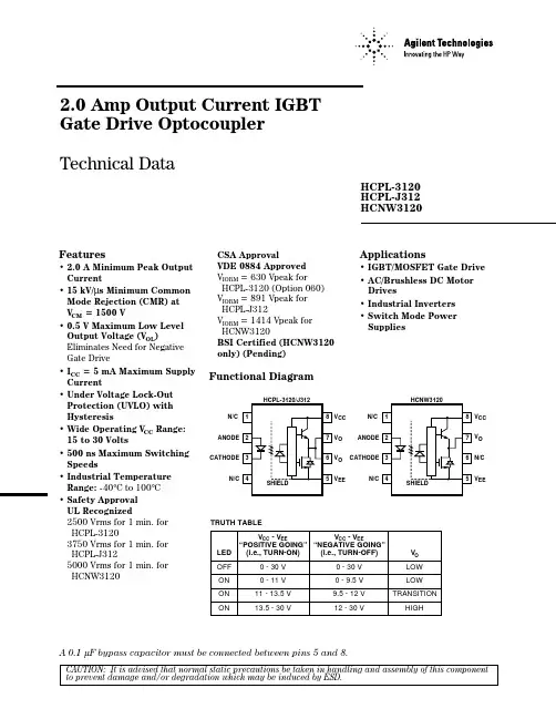
2.0 Amp Output Current IGBT Gate Drive Optocoupler Technical DataHCPL-3120HCPL-J312HCNW3120Features• 2.0 A Minimum Peak Output Current• 15 kV/µs Minimum Common Mode Rejection (CMR) at V CM = 1500 V• 0.5 V Maximum Low Level Output Voltage (V OL )Eliminates Need for Negative Gate Drive• I CC = 5 mA Maximum Supply Current• Under Voltage Lock-Out Protection (UVLO) with Hysteresis• Wide Operating V CC Range:15 to 30 Volts• 500 ns Maximum Switching Speeds• Industrial Temperature Range: -40°C to 100°C • Safety Approval UL Recognized2500 Vrms for 1 min. for HCPL-31203750 Vrms for 1 min. for HCPL-J3125000 Vrms for 1 min. for HCNW3120CSA ApprovalVDE 0884 Approved V IORM = 630 Vpeak for HCPL-3120 (Option 060)V IORM = 891 Vpeak for HCPL-J312V IORM = 1414 Vpeak for HCNW3120BSI Certified (HCNW3120only) (Pending)Applications• IGBT/MOSFET Gate Drive • AC/Brushless DC Motor Drives• Industrial Inverters • Switch Mode Power SuppliesA 0.1 µF bypass capacitor must be connected between pins 5 and 8.CAUTION: It is advised that normal static precautions be taken in handling and assembly of this componentto prevent damage and/or degradation which may be induced by ESD.Functional DiagramTRUTH TABLEV CC - V EE V CC - V EE“POSITIVE GOING”“NEGATIVE GOING”LED (i.e., TURN-ON)(i.e., TURN-OFF)V O OFF 0 - 30 V 0 - 30 V LOW ON 0 - 11 V 0 - 9.5 V LOW ON 11 - 13.5 V 9.5 - 12 V TRANSITIONON13.5 - 30 V12 - 30 VHIGH13SHIELD 248675N /CCATHODE ANODE N/C V CC V O V O V EE13SHIELD248675N /CCATHODE ANODE N/C V CC N/C V O V EEHCNW3120HCPL-3120/J312DescriptionThe HCPL-3120 contains a GaAsP LED while the HCPL-J312 and the HCNW3120 contain an AlGaAs LED. The LED is optically coupled to an integrated circuit with a power output stage. These optocouplers are ideally suited for driving power IGBTs and MOSFETs used in motor control inverter applications. The high operating voltage range of theoutput stage provides the drivevoltages required by gatecontrolled devices. The voltageand current supplied by theseoptocouplers make them ideallysuited for directly driving IGBTswith ratings up to 1200 V/100 A.For IGBTs with higher ratings,the HCPL-3120 series can beused to drive a discrete powerstage which drives the IGBT gate.The HCNW3120 has the highestinsulation voltage ofV IORM=1414Vpeak in theVDE0884. The HCPL-J312 has aninsulation voltage ofV IORM=891Vpeak and theV IORM=630Vpeak is alsoavailable with the HCPL-3120(Option060).Selection GuidePart Number HCPL-3120HCPL-J312HCNW3120HCPL-3150* Output Peak Current ( I O) 2.0 A 2.0 A 2.0 A0.5 AVDE0884 Approval V IORM=630 Vpeak V IORM=891 Vpeak V IORM=1414 Vpeak V IORM=630 Vpeak(Option 060)(Option 060)*The HCPL-3150 Data sheet available. Contact Agilent sales representative or authorized distributor.Ordering InformationSpecify Part Number followed by Option Number (if desired)Example:HCPL-3120#XXX060 = VDE0884, V IORM = 630 Vpeak (HCPL-3120 only)300 = Gull Wing Surface Mount Option500 = Tape and Reel Packaging OptionOption 500 contains 1000 units (HCPL-3120/J312), 750 units (HCNW3120) per reel.Other options contain 50 units (HCPL-3120/J312), 42 units (HCNW312) per tube.Option data sheets available. Contact Agilent sales representative or authorized distributor.(0.025 ± 0.005)MAX.(0.100)BSCDIMENSIONS IN MILLIMETERS (INCHES).LEAD COPLANARITY = 0.10 mm (0.004 INCHES).+ 0.076 - 0.051+ 0.003) - 0.002)Package Outline DrawingsHCPL-3120 and HCPL-J312 Outline Drawing (Standard DIP Package)HCPL-3120 and HCPL-J312 Gull Wing Surface Mount Option 300 Outline DrawingDIMENSIONS IN MILLIMETERS AND (INCHES).+ 0.076 - 0.051(0.010+ 0.003)- 0.002)* MARKING CODE LETTER FOR OPTION NUMBERS. "V" = OPTION 060OPTION NUMBERS 300 AND 500 NOT MARKED.1.78 ± 0.15 MAX.BSCDIMENSIONS IN MILLIMETERS (INCHES).LEAD COPLANARITY = 0.10 mm (0.004 INCHES).HCNW3120 Outline Drawing (8-Pin Wide Body Package)HCNW3120 Gull Wing Surface Mount Option 300 Outline Drawing1.78 ± 0.15 0.254+ 0.076 - 0.0051+ 0.003) - 0.002)Reflow Temperature ProfileRegulatory InformationAgency/StandardHCPL-3120HCPL-J312HCNW3120Underwriters Laboratory (UL)Recognized under UL 1577, Component RecognitionProgram, Category, File E55361Canadian Standards Association (CSA)File CA88324, per Component Acceptance Notice #5Verband Deutscher Electrotechniker (VDE)DIN VDE 0884 (June 1992)Option 060British Standards Institute (BSI)PendingCertification According to BS EN60065: 1994(BS415:1994), BS EN60950: 1992 (BS7002:1992)240TIME – MINUTEST E M P E R A T U R E – °C220200180160140120100806040200260MAXIMUM SOLDER REFLOW THERMAL PROFILE(NOTE: USE OF NON-CHLORINE ACTIVATED FLUXES IS RECOMMENDED.)Insulation and Safety Related SpecificationsValueHCPL-HCPL-HCNWParameter Symbol 3120J3123120Units ConditionsMinimum External L(101)7.17.49.6mmMeasured from input terminals to Air Gap (Clearance)output terminals, shortest distance through air.Minimum External L(102)7.48.010.0mmMeasured from input terminals to Tracking (Creepage)output terminals, shortest distance path along body.Minimum Internal 0.080.5 1.0mmInsulation thickness between emitter Plastic Gapand detector; also known as distance (Internal Clearance)through insulation.Tracking Resistance CTI >175>175>200VoltsDIN IEC 112/VDE 0303 Part 1(Comparative Tracking Index)Isolation GroupIIIa IIIa IIIaMaterial Group (DIN VDE 0110, 1/89,Table 1)VDE0884 Insulation Related CharacteristicsHCPL-3120DescriptionSymbolOption 060HCPL-J312HCNW3120UnitInstallation classification per DIN VDE 0110/1.89, Table 1for rated mains voltage ≤150 V rms I-IV I-IV I-IV for rated mains voltage ≤300 V rms I-IV I-IV I-IV for rated mains voltage ≤450 V rms I-IIII-III I-IV for rated mains voltage ≤600 V rms I-III I-IV for rated mains voltage ≤1000 V rms I-III Climatic Classification55/100/2155/100/2155/100/21Pollution Degree (DIN VDE 0110/1.89)222Maximum Working Insulation Voltage V IORM 6308911414V peak Input to Output Test Voltage, Method b*V PR118116702652V peakV IORM x 1.875 = V PR , 100% Production Test, t m = 1 sec, Partial Discharge < 5pC Input to Output Test Voltage, Method a*V PR 94513362121V peak V IORM x 1.5 = V PR , Type and SampleTest, t m = 60 sec, Partial Discharge < 5pC Highest Allowable Overvoltage*V IOTM600060008000V peak(Transient Overvoltage, t ini = 10 sec)Safety Limiting Values – maximum values allowed in the event of a failure,also see Figure 37. Case Temperature T S175175150°C Input Current I S INPUT 230400400mA Output PowerP S OUTPUT600600700mW Insulation Resistance at T S , V IO = 500 VR S≥109≥109≥109Ω*Refer to the VDE0884 section (page 1-6/8) of the Isolation Control Component Designer's Catalog for a detailed description of Method a/b partial discharge test profiles.Note: These optocouplers are suitable for “safe electrical isolation” only within the safety limit data. Maintenance of the safety data shall be ensured by means of protective circuits. Surface mount classification is Class A in accordance with CECC 00802.All Agilent data sheets report the creepage and clearance inherent to the optocoupler component itself. These dimensions areneeded as a starting point for the equipment designer whendetermining the circuit insulation requirements. However, once mounted on a printed circuit board, minimum creepage and clearance requirements must be met as specified for individual equipment standards. For creep-age, the shortest distance path along the surface of a printed circuit board between the solder fillets of the input and output leads must be considered. There are recommended techniques such as grooves and ribs which may be used on a printed circuit board to achieve desired creepage and clearances. Creepage and clearance distances will alsochange depending on factors such as pollution degree and insulation level.Absolute Maximum RatingsRecommended Operating ConditionsElectrical Specifications (DC)Over recommended operating conditions (T A = -40 to 100°C, I F(ON) = 7 to 16 mA, V F(OFF) = -3.0 to 0.8 V, V CC = 15 to 30 V, V EE = Ground) unless otherwise specified.*All typical values at T A = 25°C and V CC - V EE = 30 V, unless otherwise noted.Switching Specifications (AC)Over recommended operating conditions (T A = -40 to 100°C, I F(ON) = 7 to 16 mA, V F(OFF) = -3.0 to 0.8 V, V CC = 15 to 30 V, V EE = Ground) unless otherwise specified.*All typical values at T A = 25°C and V CC - V EE = 30 V, unless otherwise noted.Package CharacteristicsOver recommended temperature (T A = -40 to 100°C) unless otherwise specified.Parameter Symbol Device Min.Typ.Max.Units Test Conditions Fig.NoteInput-Output V ISO HCPL-31202500V RMS RH < 50%,8, 11Momentary HCPL-J3123750t = 1 min.,9, 11Withstand Voltage**HCNW31205000T A = 25°C 10, 11Resistance R I-O HCPL-31201012ΩV I-O = 500 V DC 11(Input-Output)HCPL-J312HCNW312010121013T A = 25°C1011T A = 100°CCapacitance C I-O HCPL-31200.6pF f = 1 MHz (Input-Output)HCPL-J3120.8HCNW31200.50.6LED-to-Case θLC 467°C/W Thermocouple 28Thermal Resistance LED-to-Detector θLD 442°C/W Thermal ResistanceDetector-to-Case θDC 126°C/W Thermal Resistance*All typicals at T A = 25°C.**The Input-Output Momentary Withstand Voltage is a dielectric voltage rating that should not be interpreted as an input-output continuous voltage rating. For the continuous voltage rating refer to your equipment level safety specification or Agilent Application Note 1074 entitled “Optocoupler Input-Output Endurance Voltage.”located at center underside ofpackage Notes:1. Derate linearly above 70°C free-air temperature at a rate of 0.3 mA/°C.2. Maximum pulse width = 10 µs,maximum duty cycle = 0.2%. This value is intended to allow forcomponent tolerances for designs with I O peak minimum = 2.0 A. See Applications section for additional details on limiting I OH peak.3. Derate linearly above 70°C free-air temperature at a rate of4.8 mW/°C.4. Derate linearly above 70°C free-air temperature at a rate of5.4 mW/°C.The maximum LED junction tempera-ture should not exceed 125°C.5. Maximum pulse width = 50 µs,maximum duty cycle = 0.5%.6. In this test V OH is measured with a dc load current. When driving capacitive loads V OH will approach V CC as I OH approaches zero amps.7. Maximum pulse width = 1 ms,maximum duty cycle = 20%.8. In accordance with UL1577, each optocoupler is proof tested by applying an insulation test voltage ≥3000 Vrms for 1 second (leakage detection current limit, I I-O ≤ 5 µA).9. In accordance with UL1577, each optocoupler is proof tested by applying an insulation test voltage ≥4500 Vrms for 1 second (leakage detection current limit, I I-O ≤ 5 µA).10. In accordance with UL1577, eachoptocoupler is proof tested by applying an insulation test voltage ≥6000 Vrms for 1 second (leakage detection current limit, I I-O ≤ 5 µA).11. Device considered a two-terminaldevice: pins 1, 2, 3, and 4 shorted together and pins 5, 6, 7, and 8shorted together.12. The difference between t PHL and t PLHbetween any two HCPL-3120 parts under the same test condition.13. Pins 1 and 4 need to be connected toLED common.14. Common mode transient immunity inthe high state is the maximum tolerable dV CM /dt of the common mode pulse, V CM , to assure that the output will remain in the high state (i.e., V O >15.0V).15. Common mode transient immunity ina low state is the maximum tolerable dV CM /dt of the common mode pulse,V CM , to assure that the output will remain in a low state (i.e., V O <1.0V).16. This load condition approximates thegate load of a 1200 V/75A IGBT.17. Pulse Width Distortion (PWD) isdefined as |t PHL -t PLH | for any given device.Figure 7. I CC vs. Temperature.Figure 8. I CC vs. V CC .Figure 4. V OL vs. Temperature.Figure 5. I OL vs. Temperature.Figure 6. V OL vs. I OL .Figure 1. V OH vs. Temperature.Figure 2. I OH vs. Temperature.Figure 3. V OH vs. I OH .(V O H – V C C ) – H I G H O U T P U T V O L T A G E D R O P – V-4T A – TEMPERATURE – °C -1-2-3I O H – O U T P U T HI G H C U R R E N T – AT A – TEMPERATURE – °C (V O H – V C C ) – O U T P U T H I G H V O L T A G E D R O P – VI OH – OUTPUT HIGH CURRENT – AV O L – O U T P U T L O W V O L T A G E – V0T A – TEMPERATURE – °C 0.250.050.150.200.10I O L – O U T P U T L O W C U R R E NT – AT A – TEMPERATURE – °CV O L – O U T P U T L O W V O L T A G E– VI OL – OUTPUT LOW CURRENT – A3412I C C – S U P P L Y C U R R E N T – m A1.5T A – TEMPERATURE – °C 3.02.53.52.0I C C – S U P P L Y C U R R E N T –m A1.5V CC – SUPPLY VOLTAGE – V3.02.53.52.0Figure 9. I FLH vs. Temperature.Figure 10. Propagation Delay vs. V CC .Figure 11. Propagation Delay vs. I F .Figure 12. Propagation Delay vs.Temperature.Figure 14. Propagation Delay vs. Cg.Figure 13. Propagation Delay vs. Rg.I F L H – L O W T O H I G H C U R R E N T T H R E S H O L D – m AT A – TEMPERATURE – °C 32415I F L H – L O W T O H I G H C U R R E N T T H R E S H O L D – m AT A – TEMPERATURE – °C HCPL-J312I F L H – L O W T O H I G H C U R R E N T T H R E S H O L D – m AT A – TEMPERATURE – °CHCNW3120T p – P R O P A G A T I O N D E L A Y – n s100V CC – SUPPLY VOLTAGE – V 400300500200T p – P R O P A G A T I O N D E L A Y – n s100I F – FORWARD LED CURRENT – mA 400300500200T p – P R O P A G A T I O N DE L A Y – n s100T A – TEMPERATURE – °C400300500200T p – P R O P A G A T I O N D E L A Y – n s100Rg – SERIES LOAD RESISTANCE – Ω400300500200T p – P R O P A G AT I O N D E L A Y – n s100Cg – LOAD CAPACITANCE – nF400300500200Figure 15. Transfer Characteristics.Figure 16. Input Current vs. Forward Voltage.Figure 17. I OH Test Circuit.V O – O U T P U T V O L T A G E – VI F – FORWARD LED CURRENT – mA5251513025342010HCPL-3120 / HCNW3120V O – O U T P U T V O L T A G E – V0I F – FORWARD LED CURRENT – mA1352551525341020HCPL-J31230I F – F O R W A R D C U R R E N T – m AV F – FORWARD VOLTAGE – VOLTSV F – FORWARD VOLTAGE – VOLTSI F – F O R W A R D C U R R E N T – m ACC = 15 to 30 VI F = 7 to 16 mAFigure 20. V OL Test Circuit.Figure 21. I FLH Test Circuit.Figure 19. V OH Test Circuit.Figure 18. I OL Test Circuit.Figure 22. UVLO Test Circuit.CC = 15 to 30 VCC = 15 to 30 VI F 16 mACC = 15 to 30 VCC = 15 to 30 VI FFigure 24. CMR Test Circuit and Waveforms.Figure 23. t PLH , t PHL , t r , and t f Test Circuit and Waveforms.CC = 15 to 30 V I= 30 VCM V OSWITCH AT B: I F = 0 mAV OSWITCH AT A: I F = 10 mA V OLV OHApplications InformationEliminating Negative IGBT Gate Drive (Discussion appliesto HCPL-3120, HCPL-J312, and HCNW3120)To keep the IGBT firmly off, the HCPL-3120 has a very low maximum V OL specification of 0.5V. The HCPL-3120 realizes this very low V OL by using a DMOS transistor with 1Ω(typical) on resistance in its pull down circuit. When the HCPL-3120 is in the low state, the IGBT gate is shorted to the emitter by Rg + 1Ω. Minimizing Rg and the lead inductance from the HCPL-3120 to the IGBT gate andemitter (possibly by mounting the HCPL-3120 on a small PC board directly above the IGBT) can eliminate the need for negative IGBT gate drive in many applica-tions as shown in Figure 25. Care should be taken with such a PC board design to avoid routing theIGBT collector or emitter traces close to the HCPL-3120 input as this can result in unwantedcoupling of transient signals into the HCPL-3120 and degrade performance. (If the IGBT drain must be routed near the HCPL-3120 input, then the LED should be reverse-biased when in the off state, to prevent the transient signals coupled from the IGBT drain from turning on the HCPL-3120.)Figure 25. Recommended LED Drive and Application Circuit.ACCONTROLINPUTSelecting the Gate Resistor (Rg) to Minimize IGBTSwitching Losses. (Discussion applies to HCPL-3120, HCPL-J312 and HCNW3120)Step 1: Calculate Rg Minimum from the I OL Peak Specifica-tion. The IGBT and Rg in Figure 26 can be analyzed as a simple RC circuit with a voltage supplied by the HCPL-3120.(V CC – V EE - V OL )Rg ≥–––––––––––––––I OLPEAK(V CC – V EE - 2 V )=–––––––––––––––I OLPEAK (15 V + 5 V - 2 V)=––––––––––––––––––2.5 A =7.2 Ω ≅ 8 ΩThe V OL value of 2V in the pre-vious equation is a conservative value of V OL at the peak current of 2.5A (see Figure 6). At lower Rg values the voltage supplied by the HCPL-3120 is not an ideal voltage step. This results in lower peak currents (more margin)than predicted by this analysis.When negative gate drive is not used V EE in the previous equation is equal to zero volts.Figure 26. HCPL-3120 Typical Application Circuit with Negative IGBT Gate Drive.AC- HVDCCONTROLINPUTStep 2: Check the HCPL-3120Power Dissipation and Increase Rg if Necessary. The HCPL-3120 total power dissipation (P T ) is equal to the sum of the emitter power (P E ) and the output power (P O ):P T = P E + P OP E = I F •V F •Duty CycleP O = P O(BIAS) + P O (SWITCHING)= I CC •(V CC - V EE )+ E SW (R G , Q G )•f For the circuit in Figure 26 with I F(worst case) = 16mA, Rg = 8Ω, Max Duty Cycle = 80%, Qg = 500 nC,f =20 kHz and T A max = 85C:P E = 16 mA •1.8 V •0.8 = 23 mW P O = 4.25 mA •20 V+ 5.2 µJ •20 kHz = 85 mW + 104 mW = 189 mW> 178 mW (P O(MAX) @ 85C = 250 mW −15C*4.8 mW/C)The value of 4.25 mA for I CC in the previous equation was obtained by derating the I CC max of 5 mA(which occurs at -40°C) to I CC max at 85C (see Figure 7).Since P O for this case is greater than P O(MAX), Rg must be increased to reduce the HCPL-3120 power dissipation.P O(SWITCHING MAX)= P O(MAX) - P O(BIAS)= 178 mW - 85 mW = 93 mWP O(SWITCHINGMAX)E SW(MAX)=–––––––––––––––f93 mW= ––––––– = 4.65 µW 20 kHzFor Qg = 500 nC, from Figure 27,a value of E SW = 4.65 µW gives a Rg = 10.3 Ω.P EParameterDescription I F LED Current V FLED On Voltage Duty CycleMaximum LED Duty CycleP O ParameterDescription I CC Supply Current V CC Positive Supply Voltage V EENegative Supply VoltageE SW (Rg,Qg)Energy Dissipated in the HCPL-3120 for eachIGBT Switching Cycle (See Figure 27)f Switching FrequencyFigure 27. Energy Dissipated in the HCPL-3120 for Each IGBT Switching Cycle.E s w – E N E R G Y P E R S W I T C H I N G C Y C L E – µJ0Rg – GATE RESISTANCE – Ω6144121082Thermal Model(Discussion applies to HCPL-3120, HCPL-J312and HCNW3120)The steady state thermal model for the HCPL-3120 is shown in Figure 28. The thermal resistance values given in this model can be used to calculate the tempera-tures at each node for a given operating condition. As shown by the model, all heat generated flows through θCA which raises the case temperature T Caccordingly. The value of θCAdepends on the conditions of the board design and is, therefore,determined by the designer. The value of θCA = 83°C/W wasobtained from thermal measure-ments using a 2.5 x 2.5 inch PCboard, with small traces (no ground plane), a single HCPL-3120 soldered into the center of the board and still air. The absolute maximum powerdissipation derating specifications assume a θCA value of 83°C/W.From the thermal mode in Figure 28 the LED and detector IC junction temperatures can be expressed as:T JE = P E • (θLC ||(θLD + θDC ) + θCA )θLC * θDC+ P D •(–––––––––––––––– + θCA )+ T AθLC + θDC + θLDθLC •θDCT JD = P E (––––––––––––––– + θCA)θLC + θDC + θLD+ P D •(θDC ||(θLD + θLC ) + θCA ) + T AInserting the values for θLC and θDC shown in Figure 28 gives:T JE = P E •(256°C/W + θCA ) + P D •(57°C/W + θCA ) + T A T JD = P E •(57°C/W + θCA )+ P D •(111°C/W + θCA ) + T A For example, given P E = 45 mW,P O = 250 mW, T A = 70°C and θCA = 83°C/W:T JE = P E •339°C/W + P D •140°C/W +T A= 45 mW •339°C/W + 250 m W•140°C/W + 70°C = 120°C T JD = P E •140°C/W + P D •194°C/W +T A= 45 mW •140C/W + 250 m W•194°C/W + 70°C = 125°CT JE and T JD should be limited to 125°C based on the board layout and part placement (θCA ) specific to the application.T JE =LED junction temperatureT JD =detector IC junction temperatureT C =case temperature measured at the center of the package bottom θLC =LED-to-case thermal resistance θLD =LED-to-detector thermal resistance θDC =detector-to-case thermal resistance θCA =case-to-ambient thermal resistance∗θCA will depend on the board design and the placement of the part.Figure 28. Thermal Model.θLD = 442 °C/W T JET JDθLC = 467 °C/WθDC = 126 °C/WθCA = 83 °C/W*T CT ALED Drive CircuitConsiderations for Ultra High CMR Performance.(Discussion applies to HCPL-3120, HCPL-J312, and HCNW3120)Without a detector shield, the dominant cause of optocoupler CMR failure is capacitivecoupling from the input side of the optocoupler, through the package, to the detector IC as shown in Figure 29. The HCPL-3120 improves CMR performanceby using a detector IC with an optically transparent Faraday shield, which diverts the capaci-tively coupled current away from the sensitive IC circuitry. How-ever, this shield does noteliminate the capacitive coupling between the LED and optocoup-ler pins 5-8 as shown in Figure 30. This capacitivecoupling causes perturbations in the LED current during common mode transients and becomes the major source of CMR failures forFigure 29. Optocoupler Input to OutputCapacitance Model for Unshielded Optocouplers.Figure 30. Optocoupler Input to OutputCapacitance Model for Shielded Optocouplers.a shielded optocoupler. The main design objective of a high CMR LED drive circuit becomes keeping the LED in the proper state (on or off) during common mode transients. For example,the recommended application circuit (Figure 25), can achieve 15kV/µs CMR while minimizing component complexity.Techniques to keep the LED in the proper state are discussed in the next two sections.CMR with the LED On (CMR H).A high CMR LED drive circuit must keep the LED on during common mode transients. This is achieved by overdriving the LED current beyond the input threshold so that it is not pulled below the threshold during a transient. A minimum LED cur-rent of 10 mA provides adequate margin over the maximum I FLH of 5mA to achieve 15kV/µs CMR.CMR with the LED Off(CMR L).A high CMR LED drive circuitmust keep the LED off (V F≤V F(OFF)) during common modetransients. For example, during a-dV cm/dt transient in Figure 31,the current flowing through C LEDPalso flows through the R SAT andV SAT of the logic gate. As long asthe low state voltage developedacross the logic gate is less thanV F(OFF), the LED will remain offand no common mode failure willoccur.The open collector drive circuit,shown in Figure 32, cannot keepthe LED off during a +dVcm/dttransient, since all the currentflowing through C LEDN must besupplied by the LED, and it is notrecommended for applicationsrequiring ultra high CMR Lperformance. Figure 33 is analternative drive circuit which,like the recommended applicationcircuit (Figure 25), does achieveultra high CMR performance byshunting the LED in the off state.CM • • •• • •Figure 33. Recommended LED Drive Circuit for Ultra-High CMR.Figure 31. Equivalent Circuit for Figure 25 During Common Mode Transient.Figure 32. Not Recommended Open Collector Drive Circuit.Under Voltage Lockout Feature. (Discussion applies toHCPL-3120, HCPL-J312, and HCNW3120)The HCPL-3120 contains an under voltage lockout (UVLO)feature that is designed to protect the IGBT under fault conditions which cause the HCPL-3120supply voltage (equivalent to thefully-charged IGBT gate voltage)to drop below a level necessary to keep the IGBT in a low resistance state. When the HCPL-3120output is in the high state and the supply voltage drops below the HCPL-3120 V UVLO– threshold (9.5<V UVLO– < 12.0) the opto-coupler output will go into the low state with a typical delay,UVLO Turn Off Delay, of 0.6µs.When the HCPL-3120 output is in the low state and the supply voltage rises above the HCPL-3120 V UVLO+ threshold (11.0 <V UVLO+ < 13.5) the optocoupler output will go into the high state (assumes LED is “ON”) with a typical delay, UVLO Turn On Delay of 0.8 µs.Figure 34. Under Voltage Lock Out.V O – O U T P U T V O L T A G E – V(V CC - V EE ) – SUPPLY VOLTAGE – V1014268412Figure 37. Thermal Derating Curve, Dependence of Safety Limiting Value with Case Temperature per VDE 0884.(DUE TO OPTOCOUPLER)= (t PHL MAX - t PHL MIN ) + (t PLH MAX - t PLH MIN ) = (t PHL MAX - t PLH MIN ) – (t PHL MIN - t PLH MAX ) = PDD* MAX – PDD* MIN*PDD = PROPAGATION DELAY DIFFERENCENOTE: FOR DEAD TIME AND PDD CALCULATIONS ALL PROPAGATIONDELAYS ARE TAKEN AT THE SAME TEMPERATURE AND TEST CONDITIONS.V OUT1I LED2V OUT2I LED1Figure 35. Minimum LED Skew for Zero Dead Time.Figure 36. Waveforms for Dead Time.*PDD = PROPAGATION DELAY DIFFERENCENOTE: FOR PDD CALCULATIONS THE PROPAGATION DELAYSARE TAKEN AT THE SAME TEMPERATURE AND TEST CONDITIONS.V OUT1I LED2V OUT2I LED1IPM Dead Time and Propagation DelaySpecifications. (Discussionapplies to HCPL-3120, HCPL-J312, and HCNW3120)The HCPL-3120 includes a Propagation Delay Difference (PDD) specification intended to help designers minimize “dead time” in their power inverterdesigns. Dead time is the time period during which both the high and low side powertransistors (Q1 and Q2 in Figure 25) are off. Any overlap in Q1and Q2 conduction will result in large currents flowing through the power devices between thehigh and low voltage motor rails.O U T P U T P O W E R – P S , I N P U T C U R R E N T – I S0T S – CASE TEMPERATURE – °C1000400600800200100300500700900O U T P U T P O W E R – P S , I N P U T C U R R E N T – I S0T S – CASE TEMPERATURE – °C 600400800200100300500700To minimize dead time in a given design, the turn on of LED2 should be delayed (relative to the turn off of LED1) so that under worst-case conditions, transistor Q1 has just turned off when transistor Q2 turns on, as shown in Figure 35. The amount of delay necessary to achieve this condi-tions is equal to the maximum value of the propagation delay difference specification, PDD MAX, which is specified to be 350ns over the operating temperature range of -40°C to 100°C.Delaying the LED signal by themaximum propagation delaydifference ensures that theminimum dead time is zero, but itdoes not tell a designer what themaximum dead time will be. Themaximum dead time is equivalentto the difference between themaximum and minimum propaga-tion delay difference specifica-tions as shown in Figure 36. Themaximum dead time for theHCPL-3120 is 700ns (= 350ns -(-350ns)) over an operatingtemperature range of -40°C to100°C.Note that the propagation delaysused to calculate PDD and deadtime are taken at equal tempera-tures and test conditions sincethe optocouplers under consider-ation are typically mounted inclose proximity to each other andare switching identical IGBTs.Data subject to change.Copyright © 1999 Agilent TechnologiesObsoletes 5965-4779E5965-7875E (11/99)。