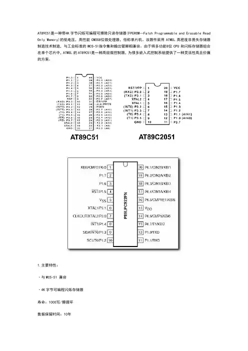
英文翻译系别专业班级学生姓名学号指导教师Introduction and application of AT89C51 Microcontrollers are used in a multitude of commercial applications such as modems, motor-control systems, air conditioner control systems, automotive engine and among others. The high processing speed and enhanced peripheral set of these microcontrollers make them suitable for such high-speed event-based applications. However, these critical application domains also require that these microcontrollers are highly reliable. The high reliability and low market risks can be ensured by a robust testing process and a proper tools environment for the validation of these microcontrollers both at the component and at the system level. Intel Plaform Engineering department developed an object-oriented multi-threaded test environment for the validation of its AT89C51 automotive microcontrollers. The goals of this environment was not only to provide a robust testing environment for the AT89C51 automotive microcontrollers, but to develop an environment which can be easily extended and reused for the validation of several other future microcontrollers. The environment was developed in conjunction with Microsoft Foundation Classes (AT89C51).The paper describes the design and mechanism of this test environment, its interactions with various hardware/software environmental components, and how to use AT89C51.1. IntroductionThe 8-bit AT89C51 CHMOS microcontrollers are designed to handle high-speed calculations and fast input/output operations. MCS 51 microcontrollers are typically used for high-speed event control systems. Commercial applications include modems, motor-control systems, printers, photocopiers, air conditioner control systems, disk drives, and medical instruments. The automotive industry use MCS 51 microcontrollers in engine-control systems, airbags, suspension systems, and antilock braking systems (ABS).The AT89C51 is especially well suited to applications that benefit from its processing speed and enhanced on-chip peripheral functions set, such as automotive power-train control, vehicle dynamic suspension, antilock braking, and stability control applications. Because of these critical applications, the market requires a reliable cost-effective controller with a low interrupt latency response, ability to service the high number of time and event driven integrated peripherals needed in real time applications, and a CPU with above average processing power in a single package. The financial and legal risk of having devices that operate unpredictably is very high. Once in the market, particularly in mission critical applications such as anautopilot or anti-lock braking system, mistakes are financially prohibitive. Redesign costs can run as high as a $500K, much more if the fix means back annotating it across a product family that share the same core and/or peripheral design flaw. In addition, field replacements of components is extremely expensive, as the devices are typically sealed in modules with a total value several times that of the component. To mitigate these problems, it is essential that comprehensive testing of the controllers be carried out at both the component level and system level under worst case environmental and voltage conditions.This complete and thorough validation necessitatesnot only a well-defined process but also a proper environment and tools to facilitate and execute the mission successfully.Intel Chandler Platform Engineering group provides postsilicon system validation (SV) of various micro-controllers and processors. The system validation process can be broken into three major parts.The type of the device and its application requirements determine which types of testing are performed on the device.The AT89C51 provides the following standard features: 4Kbytes of Flash, 128 bytes of RAM, 32 I/O lines, two 16-bittimer/counters, a five vector two-level interrupt architecture,a full duple ser -ial port, on-chip oscillator and clock circuitry.In addition, the AT89C51 is designed with static logic for operation down to zero frequency and supports two software selectable power saving modes. The Idle Mode stops the CPU while allowing the RAM, timer/counters,serial port and interrupt sys -tem to continue functioning. The Power-down Mode saves the RAM contents but freezes the oscil -lator disabling all other chip functions until the next hardware reset.Pin Configurations Block Diagram2 Pin DescriptionVCC Supply voltage.GND Ground.Port 0Port 0 is an 8-bit open-drain bi-directional I/O port. As an output port, each pin can sink eight TTL inputs. When 1s are written to port 0 pins, the pins can be used as high impedance inputs.Port 0 may also be configured to be the multiplexed low order address/data bus during accesses to external program and data memory. In this mode P0 has internal pullups.Port 0 also receives the code bytes during Flash programming, and outputs the code bytes during program verification. External pullups are required during program verification.Port 1Port 1 is an 8-bit bi-directional I/O port with internal pullups.The Port 1 output buffers can sink/so -urce four TTL inputs.When 1s are written to Port 1 pins they are pulled high by the internal pullups and can be used as inputs. As inputs, Port1 pins that are externally being pulled low will source current (IIL) because ofthe internal pullups.Port 1 also receives the low-order address bytes during Flash programming and verification.Port 2Port 2 is an 8-bit bi-directional I/O port with internal pullups.The Port 2 output buffers can sink/source four TTL inputs.When 1s are written to Port 2 pins they are pulled high by the internal pullups and can be used as inputs. As inputs, Port 2 pins that are externally being pulled low will source current (IIL) because of the internal pullups.Port 2 emits the high-order address byte during fetches from external program memory and during accesses to Port 2 pins that are externally being pulled low will source current (IIL) because of the internal pullups.Port 2 emits the high-order address byte during fetches from external program memory and during accesses to external data memory that use 16-bit addresses (MOVX @DPTR). In this application, it uses strong internal pull-ups when emitting 1s.During accesses to external data memory that use 8-bit addresses (MOVX @ RI), Port 2 emitsthe contents of the P2 Special Function Register.Port 2 also receives the high-order address bits and some control signals durin Flash programming and verification.Port 3Port 3 is an 8-bit bi-directional I/O port with internal pullups.The Port 3 output buffers can sink/sou -rce four TTL inputs.When 1s are written to Port 3 pins they are pulled high by the internal pullups and can be used as inputs. As inputs,Port 3 pins that are externally being pulled low will source current (IIL) because of the pullups. Port 3 also serves the functions of various special featuresof the AT89C51 as listed below:3 Port Pin Alternate FunctionsP3.0 RXD(serial input port)P3.1 TXD (serial output port)P3.2 INT0 (external interrupt 0)P3.3 INT1 (external interrupt 1)P3.4 T0 (timer 0 external input)P3.5 T1 (timer 1 external input)P3.6 WR (external data memory write strobe)P3.7 RD (external data memory read strobe)Port 3 also receives some control signals for Flash programming and verification. RSTReset input. A high on this pin for two machine cycles while the oscillator is running resets the device.ALE/PROGAddress Latch Enable output pulse for latching the low byte of the address during accesses to external memory. This pin is also the program pulse input (PROG)during Flash programming.In normal operation ALE is emitted at a constant rate of 1/6 the oscillator frequency, and may be used for external timing or clocking purposes. Note, however, that one ALE pulse is skipped duri -ng each access to external DataMemory.If desired, ALE operation can be disabled by setting bit 0 of SFR location 8EH. With the bit set, ALE is active only during a MOVX or MOVC instruction. Otherwise, the pin is weakly pulled high. Setting the ALE-disable bit has no effect if the microcontroller is in external execution mode.PSENProgram Store Enable is the read strobe to external program memory. When the AT89C51 is executing code from external program memory, PSEN is activated twice each machine cycle, except that two PSEN activations are skipped during each access to external data memory.EA/VPPExternal Access Enable. EA must be strapped to GND in order to enable the device to fetch code from external program memory locations starting at 0000H up to FFFFH. Note, however, that if lock bit 1 is programmed, EA will be internally latched on reset.EA should be strapped to VCC for internal program executions. This pin also receives the 12-volt programming enable voltage (VPP) during Flash programming, for parts that require 12-volt VPP.XTAL1Input to the inverting oscillator amplifier and input to the internal clock operating circuit.XTAL2Output from the inverting oscillator amplifier.4 Oscillator CharacteristicsXTAL1 and XTAL2 are the input and output, respectively, of an inverting amplifier which can be configured for use as an on-chip oscillator, as shown in Figure 1. Either a quartz crystal or ceramic resonator may be used. To drive the device from an external clock source, XTAL2 should be left unconnected while XTAL1 is driven as shown in Figure 2.There are no requirements on the duty cycle of the external clock signal, since the input to the internal clocking circuitry is through a divide-by-two flip-flop, but minimum and maximum voltage high and low time specifications must be observed.Idle ModeIn idle mode, the CPU puts itself to sleep while all the onchip peripherals remain active. The mode is invoked by software. The content of the on-chip RAM and all the special functions registers remain unchanged during this mode. The idle mode can be terminated by any enabled interrupt or by a hardware reset. It should be noted that when idle is terminated by a hard ware reset, the device normally resumes program execution, from where it left off, up to two machine cycles before the internal reset algorithm takes control. On-chip hardware inhibits access to internal RAM in this event, but access to the port pins is not inhibited. To eliminate the possibility of an unexpected write to a port pin when Idle is terminated by reset, theinstruction following the one that invokes Idle should not be one that writes to a port pin or to external memory.Figure 1. Oscillator Connections Figure 2. External Clock Drive Configuration Note: C1, C2 = 30 pF . .10 pF for Crystals = 40 pF . .10 pF for Ceramic Resonators In the power-down mode, the oscillator is stopped, and the instruction that invokes.5 Power-down Modepower-down is the last instruction executed. The on-chip RAM and Special Function Registers retain their values until the power-down mode is terminated. The only exit from power-down is a hardware reset. Reset redefines the SFRs but does not change the on-chip RAM. The reset should not be activated before VCC is restored to its normal operating level and must be held active long enough to allow the oscillator to restart and stabilize.Status of External Pins During Idle and Power-down Modes Mode Program Memory ALE PSEN PORT0 PORT1 PORT2 PORT3Idle Internal 1 1 Data Data Data DataIdle External 1 1 Float Data Address DataPower-down Internal 0 0 Data Data Data DataPower-down External 0 0 Float Data Data DataProgram Memory Lock BitsOn the chip are three lock bits which can be left unprogrammed (U) or can be programmed (P) to obtain the additional features listed in the table below.Lock Bit Protection Modes Program Lock Bits Protection Type LB1 LB2 LB31 U U U No program lock features2 P U U MOVC instructions executed from external program memory are disabled from etching code bytes from internal memory.3 P P U Same as mode 2, also verify is disabled4 P P P Same as mode 3, also external execution is disabledWhen lock bit 1 is programmed, the logic level at the EA pin is sampled and latched during reset. If the device is powered up without a reset, the latch initializes to a random value, and holds that value until reset is activated. It is necessary that the latched value of EA be in agreement with the current logic level at that pin in order for the device to function properly.6 Programming the FlashThe AT89C51 is normally shipped with the on-chip Flash memory array in the erased state (that is, contents = FFH) and ready to be programmed. The programming interface accepts either a high-voltage (12-volt) or a low-voltage (VCC) program enable signal. The low-voltage programming mode provides a convenient way to program the AT89C51 inside the user’s system, while the high-voltage programming mode is compatible with conventional thirdparty Flash or EPROM programmers. The AT89C51 is shipped with either the high-voltage or low-voltage programming mode enabled. The respective top-side marking and device signature codes are listed in the following table.VPP = 12V VPP = 5VTop-Side Mark AT89C51 AT89C51xxxx xxxx-5yyww yywwSignature (030H) = 1EH (030H) = 1EH(031H) = 51H (031H) = 51H(032H) =F FH (032H) = 05HThe AT89C51 code memory array is programmed byte-bybyte in either programming mode. To program any nonblank byte in the on-chip Flash Memory, the entire memory must be erased using the Chip Erase Mode.7 Programming AlgorithmBefore programming the AT89C51, the address, data and control signals should be set up according to the Flash programming mode table and Figure 3 and Figure 4. To program the AT89C51, take the following steps.1. Input the desired memory location on the address lines.2. Input the appropriate data byte on the data lines.3. Activate the correct combination of control signals.4. Raise EA/VPP to 12V for the high-voltage programming mode.5. Pulse ALE/PROG once to program a byte in the Flash array or the lock bits. The byte-write cycle is self-timed and typically takes no more than 1.5 ms. Repeat steps 1 through 5, changing the address and data for the entire array or until the end of the object file is reached.Data Polling:The AT89C51 features Data Polling to indicate the end of a write cycle. During a write cycle, an attempted read of the last byte written will result in the complement of the written datum on PO.7. Once the write cycle has been completed, true data are valid on all outputs, and the next cycle may begin. Data Polling may begin any time after a write cycle has been initiated.Ready/Busy:The progress of byte programming can also be monitored by the RDY/BSY output signal. P3.4 is pulled low after ALE goes high during programming to indicate BUSY. P3.4 is pulled high again when programming is done to indicateREADY.Program Verify: If lock bits LB1 and LB2 have not been programmed, the programmed code data can be read back via the address and data lines for verification.The lock bits cannot be verified directly. Verification of the lock bits is achieved by observing that their features are enabled.8 Flash Programming ModesMode RST PSEN ALE/PROG EA/VPP P2.6 P2.7 P3.6 P3.7Write Code Data H L H/12V L H H HRead Code Data H L H H L L H HWriteLockBit -1 H L H/12V H H H HBit -2 H L H/12V H H L LBit -3 H L H/12V H L L LChip Erase H LH/12V H L L LRead Signature Byte H L H H L L L LNote: 1. Chip Erase requires a 10 ms PROG pulse.Figure 3. Programming the Flash Figure 4. Verifying the FlashFlash Programming and Verification Waveforms -High-voltage Mode (VPP = 12V) Flash Programming and Verification Waveforms -Low-voltage Mode (VPP = 5V)9 Chip EraseThe entire Flash array is erased electrically by using the proper combination of control signals and by holding ALE/PROG low for 10 ms. The code array is written with all “1”s. The chip erase operation must be executed befor e the code memory can be re-programmed.Reading the Signature Bytes:The signature bytes are read by the same procedure as a normal verification of locations 030H, 031H, and 032H, except that P3.6 and P3.7 must be pulled to a logic low. The values returned areas follows.(030H) = 1EH indicates manufactured by Atmel(031H) = 51H indicates 89C51(032H) = FFH indicates 12V programming(032H) = 05H indicates 5V programmingProgramming InterfaceEvery code byte in the Flash array can be written and the entire array can be erased by using the appropriate combination of control signals. The write operation cycle is selftimed and once initiated, will automatically time itself to completion. Flash Programming and Verification Characteristics TA = 0°C to 70°C, VCC = 5.0 . .10%10 Symbol Parameter Min Max UnitsVPP(1) Programming EnableV oltage11.5 12.5 VIPP(1) Programming Enable Current 1.0 mA1/tCLCL Oscillator Frequency 3 24 MHztA VGL Address Setup to PROGLow48tCLCLtGHAX Address Hold After PROG 48tCLCLtDVGL Data Setup to PROG Low 48tCLCLtGHDX Data Hold After PROG 48tCLCLtEHSH P2.7(ENABLE) High to VPP 48tCLCLtSHGL VPP Setup to PROG Low 10 μstGHSL(1) VPP Hold After PROG 10 μstGLGH PROG Width 1 110 μstA VQV Address to Data Valid 48tCLCLtELQV ENABLE Low to Data Valid 48tCLCLtEHQZ Data Float After ENABLE 0 48tCLCLtGHBL PROG High to BUSY Low 1.0 μstWC Byte Write Cycle Time 2.0 msNote: 1. Only used in 12-volt programming mode.Absolute Maximum Ratings*Operating Temperature......................... -55°C to +125°CStorage Temperature ............................. -65°C to +150°CV oltage on Any Pin with Respect to Ground ............-1.0V to +7.0VMaximum Operating V oltage .................................. 6.6VDC Output Current....................................... 15.0 mA11 DC CharacteristicsTA = -40°C to 85°C, VCC = 5.0V . .20% (unless otherwise noted)Symbol Parameter Condition Min Max Units VIL Input Low-voltage (Except EA) -0.5 0.2 VCC 0.1 -VVIL1 nput Low-voltage (EA) -0.5 0.2 VCC 0.3 -VVIH iput High-voltage (Except XTAL1, RST) 0.2 VCC +0.9 VCC + 0.5 VVIH1 Input High-voltage (XTAL1, RST) 0.7 VCC VCC + 0.5 VVOL Output Low-voltage(1) (Ports 1,2,3) IOL = 1.6 mA 0.45 VVOL1 Output Low-voltage(1) (Port 0, ALE, PSEN) IOL = 3.2 mA 0.45 VVOH Output High-voltage (Ports 1,2,3, ALE, PSEN) IOH = -60 μA, VCC = 5V . .10% 2.4 VIOH = -25 μA 0.75 VCC VIOH = -10 μA 0.9 VCC VVOH1 Output High-voltage (Port 0 in External Bus Mode) IOH = -800 μA, VCC = 5V . .10% 2.4 VIOH = -300μA, 0.75 VCC VIOH = -80μA, 0.9 VCC VIIL Logical 0 Input Current (Ports 1,2,3)VIN = 0.45V -50 μ AITL Logical 1 to 0 Transition Current (Ports 1,2,3) VIN = 2V, VCC = 5V . .10% -650 μ AILI Input Leakage Current (Port 0, EA) 0.45 < VIN < VCC . 10 μ A RRST Reset Pull-down Resistor 50 300 K.CIO Pin Capacitance Test Freq. = 1 MHz, TA = 25°C 10 pFICC Power Supply Current Active Mode, 12 MHz 20 mA Idle Mode, 12 MHz 5 mA Power-down Mode(2) VCC = 6V 100 μ A VCC = 3V 40 μ A12 AC CharacteristicsUnder operating conditions, load capacitance for Port 0, ALE/PROG, and PSEN = 100 pF; load capacitance for all other outputs = 80 pF.External Program and Data Memory Characteristics Symbol ParameterFrequency 12 MHz Oscillator 16 to 24 MHz Oscillator Units Min Max Min Max 1/tCLCL Oscillator 0 24 MHztLHLL ALE Pulse Width 127 2tCLCL-40 40 ns nstA VLL Address Valid to ALE Low 43 tCLCL-13 nstLLAX Address Hold After ALE Low 48 tCLCL-20 nstLLIV ALE Low to Valid Instruction In 233 4tCLCL-65 nstLLPL ALE Low to PSEN Low 43 tCLCL-13 nstPLPH PSEN Pulse Width 205 3tCLCL-20 nstPLIV PSEN Low to Valid Instruction In 145 3tCLCL-45 nstPXIX Input Instruction Hold After PSEN 0 0 nstPXIZ Input Instruction Float After PSEN 59 tCLCL-10 nstPXA V PSEN to Address Valid 75 tCLCL-8 nstA VIV Address to Valid Instruction In 312 5tCLCL-55 nstPLAZ PSEN Low to Address Float 10 10 nstRLRH RD Pulse Width 400 6tCLCL-100 nstWLWH WR Pulse Width 400 6tCLCL-100 nstRLDV RD Low to Valid Data In 252 5tCLCL-90 nstRHDX Data Hold After RD 0 0 ns 13tRHDZ Data Float After RD 97 2tCLCL-28 nstLLDV ALE Low to Valid Data In 517 8tCLCL-150 nstA VDV Address to Valid Data In 585 9tCLCL-165 nstLLWL ALE Low to RD or WR Low 200 300 3tCLCL-50 3tCLCL+50 nstA VWL Address to RD or WR Low 203 4tCLCL-75 nstQVWX Data Valid to WR Transition 23 tCLCL-20 nstQVWH Data Valid to WR High 433 7tCLCL-120 nstWHQX Data Hold After WR 33 tCLCL-20 nstRLAZ RD Low to Address Float 0 0 nstWHLH RD or WR High to ALE High 43 123 tCLCL-20 nsExternal Program Memory Read CycleExternal Data Memory Read CycleExternal Data Memory Write Cycle External Data Memory Write CycleExternal Clock Drive WaveformsExternal Clock DriveSymbol Parameter Min Max Units1/tCLCL Oscillator Frequency 0 24 MHztCLCL Clock Period 41.6 nstCHCX High Time 15 nstCLCX Low Time 15 nstCLCH Rise Time 20 nstCHCL Fall Time ns 20 nsSerial Port Timing:Shift Register Mode Test Conditions(VCC = 5.0 V . .20%; Load Capacitance = 80 pF)Symbol Parameter 12 MHz Osc Variable Oscillator Units UnitsMin Max Min MaxtXLXL Serial Port Clock Cycle Time 1.0 12tCLCL μstQVXH Output Data Setup to Clock Rising Edge 700 10tCLCL-133 nstXHQX Output Data Hold After Clock Rising Edge 50 2tCLCL-117 nstXHDX Input Data Hold After Clock Rising Edge 0 0 nstXHDV Clock Rising Edge to Input Data Valid 700 10tCLCL-133 ns 13 ShiftRegister Mode Timing Waveforms AC Testing Input/Output Waveforms Float WaveformsA microcomputer interface converts information between two forms. Outside the microcomputer the information handled by an electronic system exists as a physical signal, but within the program, it is represented numerically. The function of any interface can be broken down into a number of operations which modify the data in some way, so that the process of conversion between the external and internal forms is carried out in a number of steps.An analog-to-digital converter(ADC) is used to convert a continuously variable signal to a corresponding digital form which can take any one of a fixed number of possible binary values. If the output of the transducer does not vary continuously, no ADC is necessary. In this case the signal conditioning section must convert the incoming signal to a form which can be connected directly to the next part of the interface, the input/output section of the microcomputer itself.Output interfaces take a similar form, the obvious difference being that here the flow of information is in the opposite direction; it is passed from the program to the outside world. In this case the program may call an output subroutine which supervises the operation of the interface and performs the scaling numbers which may be needed for a digital-to-analog converter(DAC). This subroutine passes information in turn to an output device which produces a corresponding electrical signal, which could be converted into analog form using a DAC. Finally the signal is conditioned(usually amplified) to a form suitable for operating an actuator.The signals used within microcomputer circuits are almost always too small to be connected directly to the “outside world” and some kind of interface must be used to translate them to a more appropriate form. The design of section of interface circuits is one of the most important tasks facing the engineer wishing to apply microcomputers. We have seen that in microcomputers information is represented as discrete patterns of bits; this digital form is most useful when the microcomputer is to be connected to equipment which can only be switched on or off, where each bit might represent the state of a switch or actuator.To solve real-world problems, a microcontroller must have more than just a CPU, a program, and a data memory. In addition, it must contain hardware allowing the CPU to access information from the outside world. Once the CPU gathers information and processes the data, it must also be able to effect change on some portion of the outside world.These hardware devices, called peripherals, are the CPU’s window to theoutside. The most basic form of peripheral available on microcontrollers is the general purpose I70 port. Each of the I/O pins can be used as either an input or an output. The function of each pin is determined by setting or clearing corresponding bits in a corresponding data direction register during the initialization stage of a program. Each output pin may be driven to either a logic one or a logic zero by using CPU instructions to pin may be viewed (or read.) by the CPU using program instructions.Some type of serial unit is included on microcontrollers to allow the CPU to communicate bit-serially with external devices. Using a bit serial format instead of bit-parallel format requires fewer I/O pins to perform the communication function, which makes it less expensive, but slower. Serial transmissions are performed either synchronously or asynchronously.AT89C51的介绍及运用单片机广泛应用于商业:诸如调制解调器,电动机控制系统,空调控制系统,汽车发动机和其他一些领域。