
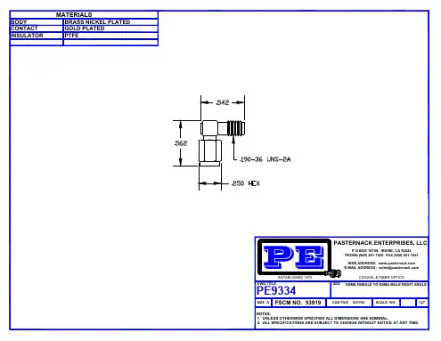
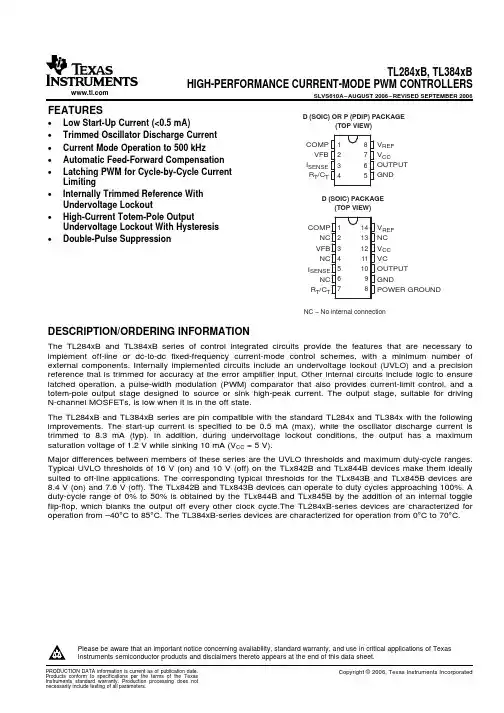
PE9334中文资料
- 格式:pdf
- 大小:19.83 KB
- 文档页数:1

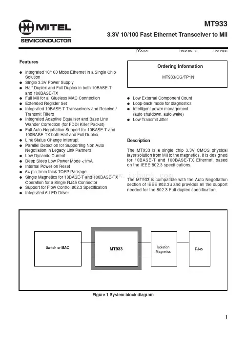
FeaturesG Integrated 10/100 Mbps Ethernet in a Single Chip SolutionG Single 3.3V Power SupplyG Half Duplex and Full Duplex in both 10BASE-T and 100BASE-TXG Full MII for a Glueless MAC Connection G Extended Register SetG Integrated 10BASE-T Transceivers and Receive /Transmit FiltersG Integrated Adaptive Equaliser and Base Line Wander Correction (for FDDI Killer Packet)G Full Auto-Negotiation Support for 10BASE-T and 100BASE-TX both Half and Full DuplexG Link Status Change InterruptG Parallel Detection for Supporting Non Auto Negotiation in Legacy Link Partners G Low Dynamic CurrentG Deep Sleep Low Power Mode <1mA G Internal Power on ResetG 64 pin 1mm thick TQFP PackageG Single Magnetics for 10BASE-T and 100BASE-TX Operation for a Single RJ45 ConnectorG Support for Flow Control 802.3 Specification GIntegrated 6 LED DriverDS5029Issue no 3.0June 2000Ordering InformationMT933/CG/TP1NDescriptionThe MT933 is a single chip 3.3V CMOS physical layer solution from MII to the magnetics. It is designed for 10BASE-T and 100BASE-TX Ethernet, based on the IEEE 802.3 specifications.The MT933 is compatible with the Auto Negotiationsection of IEEE 802.3u and provides all the supportneeded for the 802.3 Full duplex specification.Figure 1 System block diagramG Low External Component Count G Loop-back mode for diagnostics G Intelligent power management (auto shutdown, auto wake)GLow Transmit Jitterhttps://Figure 2Pin connectionsTP6448 MINT 47 DVDD346 MDC 45 MDIO 44 DGND343 RefCLK 42 OSCVDD 41 XTAL140 XTAL239 OSCGND 38 TXGND437 TXVDD436 TXREF10035 TXREF1034 TXVDD333 TXGND3S U B G N D 1 32P A 0 31P A 1 30P A 2 29T X O N 28T X V D D 1 27T X G N D 1 26T X G N D 2 25T X V D D 2 24T X O P 23A N E N 22R X V D D 1 21R X I N 20 R X I P 19R X G N D 1 18P A 3 17RXGND2 16RXVDD2 15RESETN 14PA4 13SPDST 12FDST 11RXGND3 10RXVDD3 9DVDD1 8COLST 7ACTST 6LNKST 5TX_EN 4DGND1 3TX_ER 2SUBGND2 164 T X _C L K 63 T X 0362 T X D 261 T X D 160 T X D 059 R X _E R 58 R X D 357 R X D 256 R X D 155 R X D 054 D V D D 253 R X _C L K 52 D G N D 251 R X _D V 50 C R S 49 C O LFunctional DescriptionThe MT933 has three basic modes of operation:10BASE-T, 100BASE-TX and LOW POWER modes.The Control block is designed to manage these modes by starting and stopping the 10M and 100M transceivers in a well-controlled manner such that no spurious signals are output on either the MII or twisted-pair interfaces. Furthermore, it continuously monitors the behaviour of the transceivers and takes corrective action if a fault is detected.Other modes described herein are repeater mode and reset mode.25MHz Reference ClockThe MT933 requires a 25MHz +/-100ppm timing reference for 802.3 compatible operation. This may be supplied either from the integrated oscillator or from an external source. When the integrated oscillator is used, a suitable crystal must be connected across the XTAL1 & XTAL2 pins (see “External Components”)and REFCLK must be tied low. When an external source is used, it must be input to the REFCLK pin and XTAL1 must be tied low. XTAL2 must be unconnected.10Base-T Operation10Mb/s Data Transfer on the MII10Mb/s data is transferred across the MII with clock speeds of 2.5MHz. The MAC outputs data to the MT933 via the MII interface, on the TXD[3:0] bus.This data is synchronised to the rising edge of TX_CLK. To indicate that there is valid data for transmission on the MII, the MAC sets the TX_EN signal active. This forces the MT933 device to take in the data on the TXD[3:0] bus. This is serialised and directly encoded as Manchester data, before being output on the TXOP/TXON differential output for transmission through 1:Ö2 magnetics and onto the twisted-pair.The transmit current is governed by the current through the TXREF10 pin, which must be grounded through a resistor as described in “External Components”.RX10 Clock RecoveryThe MT933 employs a digital delay line controlled by the 100MHz Synthesizer DLL to derive a sampling clock from the incoming signal. The recovered clock runs at twice the data rate (nominally 20MHz). When a signal is received from the Signal Detect block, it is used to strobe Link Pulses and Manchester encoded serial data.https://The Manchester data stream will be decoded into a 4-bit parallel data bus, RXD[3:0]. The RXD bus is clocked out on RX_CLK rising. The MT933 must detect the first 4 bits of pre-amble before RX_DV is set high. When RX_DV is high, any Manchester coding violation will set RX_ER high. RX_DV is reset by a continuous sequence of zeroes, or by the end-of-packet IDLE terminator (11 11 00 00). Whilst RX_DV is low, the data is invalid.100MHz SynthesizerThis synthesizer employs a delay-locked loop (DLL) to generate a 100MHz timing reference from the 25MHz reference clock. This 100MHz reference is used by the 10BASE-T transmit and receive functions and is divided by 5 to provide a 20MHz data strobe. The 20MHz clock is used to derive the 2.5 MHz TX_CLK in 10BASE-T mode. The synthesizer is disabled when not in 10BASE-T mode.TX10 Pulse Shaper & FilterThe Pulse Shaper & Filter employs a digital Finite Impulse Response filter (FIR) to pre-compensate for line distortion and to remove high frequency components in accordance with the 802.3 Standard. The Pulse Shaper & Filter is disabled when not in 10BASE-T mode.TX10 LatencyWhen connected to appropriate magnetics the latency through the TX10 path is less than 2BT (200ns) for data transmissions. This timing is measured from the rising edge of TX_CLK to the output of the transmit magnetics. The TX10 path will not transmit up to the first two Manchester encoded bits of a data transmission, as permitted by the 802.3 Standard. RX10 Filter & RX10 Signal DetectThese blocks work in unison to remove noise and to block signals that do not achieve the voltage levels specified in 802.3. Signals that do not achieve the required level are not sampled in the Clock Recovery block and are not passed to the outputs.RX10 LatencyWhen connected to appropriate magnetics the latency through the RX10 path is less than 6BT (600ns). This timing is measured from the input of the receive magnetics to the rising edge of RX_CLK. The RX10 path may ignore up to three Manchester encoded bits at the start of data reception (802.3 allows up to 5 bits).100Base-TX Operation100Mb/s Data Exchange on the MII Interface100Mb/s data is transferred across the MII with clock speeds of 25MHz. The MAC outputs data to the MT933 via the MII interface, on the TXD[3:0] bus. This data is synchronised to the rising edge of TX_CLK. To indicate that there is valid data for transmission on the MII, the MAC sets the TX_EN signal active. This forces the MT933 device to take in the data on the TXD[3:0] bus and replace the first octet of the MAC preamble with Start-of-Stream Delimiter (SSD) symbols to indicate the start of the Physical Layer Stream.When the data transfer across the MII is complete, the MAC deasserts the TX_EN signal and the MT933 adds End-of-Stream Delimiters (ESD) symbols onto the end of the data stream. The complete data stream (the Physical Layer Stream) is encoded from 4 bits into 5 bits, scrambled, converted to MLT3 and driven to the TXOP and TXON pin differentially.The TX100 path is disabled when not in 100BASE-TX mode and, with the exception of the RX100 Signal Detect, the RX100 Receive Path is disabled when not in 100BASE-TX mode.125MHz SynthesizerThis synthesizer employs a phase-locked loop (PLL) to generate a 125MHz timing reference from the 25MHz reference clock. This 125MHz reference is used by the 100BASE-TX transmit function and is divided by 5 to provide a 25MHz data strobe on TX_CLK. TX_CLK is frequency and phase locked to the 25MHz reference with a small phase offset. The synthesizer is disabled when not in 100BASE-TX mode.https://TX100 PISO, Encoder and ScramblerData from the MII is loaded into the TX100 PISO, Encoder and Scrambler on the rising edge of TX_CLK. It is converted to serial MLT3 for outputting to the TX100 Driver. The TXD[3] bit is output first. The PISO & Encoder do not operate until the 125MHz Synthesizer is locked to the 25MHz reference. This avoids transmission of spurious signals onto the twisted-pair.TX100 DriverThe TX100 Driver outputs the differential signal onto the TXOP and TXON pins. It operates with 1:root 2 magnetics to provide impedance matching and amplification of the signal in accordance with the 802.3 specifications. The transmit current is governed by the current through the TXREF100 pin, which must be grounded through a resistor as described in “External Components”. The TX100 driver is disabled in 10BASE-T mode and in loop back mode.If no data is being transmitted from the MAC, the MT933 outputs idle symbols of 11111 (suitably scrambled).TX100 LatencyThe transmit latency from the first TX_CLK rising when TX_EN is high to the first bit of the “J” symbol on the cable is 8BT.RX100 Equalizer & Base-line Wander CorrectionThe RX100 Equalizer compensates for the signal attenuation and distortion resulting from transmission down the cable and through the isolation transformers. The Equalizer is self-adjusting and is designed to restore signals received from up to 10dB cable attenuation (at 16MHz). When the Equalizer is active it adjusts to the incoming signal within 1ms. Thereafter, the Equalizer will continuously adjust to small variations in signal level without corrupting the received data.The 100BASE-TX MLT3 code contains significant low frequency components which are not passed through the isolation transformers and cannot be restored by an adaptive equalizer. This leads to a phenomenon known as Base-line Wander which will cause an unacceptable increase in error rate if not corrected. The MT933 employs a quantized feedback technique to restore the low frequency components and thus maintain a very low error rate even when receiving signals such as the “killer packet”described in the TP_PMD spec.RX100 Clock RecoveryThe RX100 Clock Recovery circuit uses a Phase-Locked Loop (PLL) to derive a sampling clock from the incoming signal. The recovered clock runs at the symbol bit rate rate (nominally 125MHz) and is used to clock the MLT3 decoder and the Serial to Parallel converter (SIPO).The recovered clock is divided by 5 to generate the receive clock (RX_CLK) which is used to strobe received data across the MII interface. When no signal is detected in 100BASE-TX mode, the PLL is locked to the reference clock and runs at 125MHz. This ensures that RX_CLK runs continuously at 25MHz in 100BASE-TX mode. When a signal is present, the Clock Recovery PLL remains locked to the reference until the equalizer has adjusted, then it requires up to 1ms to phase lock to the incoming signal. No data is passed to the MII interface until lock is established.RX100 SIPO, Decoder and DescramblerThe RX100 SIPO, Decoder and Descrambler convert the received signal from serial MLT3 to 4-bit wide parallel receive data on the MII. This appears on the RXD[3:0] bus which is clocked out on the falling edge of RX_CLK. When a frame starts the MT933 decodes the SSD symbols and then asserts the RX_DV signal, in order to inform the MAC that valid data is available. When the MT933 detects the ESD, it deasserts the RX_DV signal.RX100 LatencyThe latency from the first bit of the “J” symbol on the cable to CRS assertion is between 11 and 15BT. The latency from the first bit of the “T” symbol on the cable to CRS de-assertion is between 19 and 23BT. 100Mb/s Transmit ErrorsIf the MT933 detects that the TX_ER signal has gone active whilst the TX_EN signal is active, then it will propagate the detected error onto the cable by transmitting the symbol “00100” . Figure 3 shows the meaning of the different states of TX_EN and TX_ER. TX_ER is sampled inside the MT933 on the rising edge of TX_CLK.https://100Mb/s Receive ErrorsWhen there is no data on the cable, the receiver will see only the idle code of scrambled 1’s. If a non idle symbol is detected, the receiver looks for the SSD so that it can align the incoming message for decoding.If any 2 non consecutive zeros are detected within 10bits, but are not the SSD symbols a false carrier indication is signalled to the MII by asserting RX_ER and setting RXD[3:0] to 1110 whilst keeping RX_DV inactive. The remainder of the message is ignored until 10 bits of 1’s are detected.If any data is decoded after a SSD which is neither a valid data code nor an ESD, then an error is flagged by setting RX_ER active whilst the RX_DV signal is active. This also happens if 2 idle codes are detected before a valid ESD has been received or descramble synchronisation is lost during packet reception. The states of RX_DV and RX_ER are summarised in Figure 4. RX_ER is clocked on the falling edge of RX_CLK, and will remain active for at least 1 period of RX_CLK.RX_DV RX_ER RXD [3:0]Indication 000000 through 1111Normal inter frame 011110False carrier indication 100000 through 1111Normal data reception 110101 or 0110Data reception with errorsFigure 4. 100Mb/s receive error statesCONTROLSInitialization, mode selection and other options are governed by the control inputs and register as described in the following paragraphs.TX_EN TX_ER TXD [3:0]Indication0X ignored Normal inter frame data 100000 through 1111Normal data transmission 110000 through 1111Transmit error propagationFigure 3. 100Mb/s Transmit Error StatesInitialization (RESET_N)The MT933 incorporates a power-on-reset circuit for self-initialization on power-up. During initialization the open-drain RESET_N pin is driven low and all data outputs are disabled to prevent spurious outputs to the twisted-pair and to the MII interface. RESET_N will remain low until the power supply has been stable for at least 400ns. The MT933 will then release RESET_N allowing the external pull-up to pull the pin high. Device initialisation will not commence until RESET_N is high. This allows the user to extend the inactive period by externally holding RESET_N low.It will not normally be necessary for the user to reset the MT933 because it is designed to automatically recover from fault conditions. However, if required,the user may initialize the device by doing a hardware or software reset.Reset ModeThere are two types of reset in the MT933 - hardware and software. The hardware reset is activated by setting the RESET_N pin to logic 0, and holding it low for at least 100ns. This mode causes an over-all reset in the MT933 - both analog and digital circuitry are reset. Whilst RESET_N is low, the SPDST and FDST pins are inputs, and are used to determine the speed and duplex capability which will be advertised during auto-neg. A low on SPDST advertises 100M capability.A high on FDST advertises full duplex capability.The software reset is activated by setting bit 15 in register 0 high. This bit is a self clear bit and causes a partial reset of the device.Figure 5 summarises the different blocks to be reset and which reset will affect them:BlockHW ResetSW reset management register yes yes PCS state machine (RCV,yes yes XMT, ANEG)XMT scrambler yes yes RCV scramble yes yes control state machine yes No analogyesNoFigure 5. Effects of ResetNote: Holding RESET_N low will hold the device in a static,low power state.https://Low-Power ModeThis function is set via the management interface. Using MDC and MDIO, Bit 11 of register 0 is written high to put the MT933 into Low-Power mode. The type of low power mode is dependant on bits 14 and 15 in register 24.For 24[15:14] = 0:0 the 10BASE-T and 100BASE-TX transceivers are disabled. The oscillator continues to run. Both RX_CLK and TX_CLK are stopped, the RXD bus is held low and TXD, TXEN, and TXER are ignored. MDC and MDIO are still active for new commands. This mode is intended to conserve power when the network connection is not required and the TXOP/TXON output is undriven. Typical current consumption is less than 10mA.For 24[15:14] = 0:1, everything is turned off, including the voltage references and the oscillator. This mode must be exited via the management interface. Typical current consumption is 0.5mA.For 24[15:14] = 1:0, the only function available is the signal detect. The MT933 will detect a signal amplitude on the cable and activate the interrupt. MINT can be selected as either an active low or high interrupt. Typical current consumption is less than 10mA. For 24[15:14] = 1:1, the MT933 will automatically power down into a sleep mode if no activity is seen on the cable for approx 2 seconds. Power up is also automatic if activity is seen. Typical current consumption is less than 10mA.Loopback ModeDiagnostic loopback may be selected at any time by asserting setting Bit 14 in register 0. In 10BASE-T mode transmission to the TXOP/ TXON output will be stopped and the RX10 Clock Recovery will receive input from the TX10 transmit path rather than from the RXIP/RXIN inputs. In 100BASE-TX mode transmission to the TXOP/TXON output will be stopped and the RX100 Clock Recovery will receive input from the TX100 transmit path.Repeater ModeThe MT933 can be put into Repeater Mode by setting register 24 bit 0 high. In this mode, the CRS will be active on receive only. In 100Mbps repeater mode, the MT933 is able to perform a disconnect function from the MII. This function is enabled by bit 1 in register 24. (Note that if the device is not in repeater mode, this bit has no effect). The MT933 will disconnect from the MII if it receives two consecutive false CRS events with no good frame in between them or if a false CRS event is longer then 480 +/- 4BT. If the MT933 receives a good carrier event (480 +/- 4BT) or a good idle event (idle symbols for a period of 25000 to 30000 bit time) it will resume frame transfer to the MII.A false CRS event happens if, at the beginning of a carrier event, the JK symbols are not received correctly.When the MT933 is in 100M mode it will count all false CRS events in register 27 bits 7:0. This counter is self cleared upon read. If a disconnect event occurs between the consecutive reads of register 27, bit 15 in the register will set high.Auto-Negotiation Enable (ANEN)Auto-negotiation may be hardware disabled by setting the ANEN pin to logic zero. During operation, auto-negotiation can be disabled by setting the ANEN pin low or by setting bit 12 of register 0 to zero. If auto-neg is disabled, the MT933 will lose the link, and link will be re-established only after the MT933 control state machine has determined the speed using bits 13 and 8 of register 0 to determine speed and duplex respectively.MII Management Interface, MDC and MDIO The management interface is a 2 wire serial interface connecting a PHY to a management entity. The management unit controls the PHY and gathers information on the status of the PHY. It does this via the implemented registers using MDC to clock the data on the MDIO pin.Link Status Change Interrupt, MINTMINT is, by default, an active low interrupt which is activated whenever a change in the link status occurs. It can be changed to be active high by setting bit 13 in register 24. The interrupt will remain active until the controller acknowledges the interrupt by writing to register 21 (any data). Should one or more link status changes occur between the assertion of MINT and an ackowledge, then MINT will be deasserted and then reasserted (deassertion time between 100ns and 150ns). Only a single interrupt event may be queued at any one time. Multiple status changes between an ackowledge will generate only a single queued interrupt.https://Figure 6 MT933 block diagramPin listPin #Name Type DescriptionMD interface20RXIN Input Differential receive pair from magnetics (-)19RXIP Input Differential receive pair from magnetics (+)28TXON Output100 Differential transmit pair to magnetics (-)23TXOP Output100 Differential transmit pair to magnetics (+)35TXREF10Input10BASE-T transmitter current setting pin36TXREF100Input100BASE-TX transmitter current setting pin14RESETN IOput Active low, power on reset output and external reset input41XTAL1Input25MHz crystal input40XTAL2Input25MHz crystal inputMII interface46MDC Input Management interface clock (up to 2.5MHz)45MDIO IOput Management data53RX_CLK Output Receive clock (2.5MHz for 10, 25MHz for 100)55, 56, 57, 58RXD0, RXD1,Output Receive data MII interaceRXD2, RXD351RX_DV Output Receive data valid. Active high.59RX_ER Output Receive error. Active high. (RXD4 in symbol mode)43REFCLK Input Reference clock64TX_CLK Output Transmit clock (2.5MHz for 10, 25MHz for 100)60, 61, 62, 63TXD0, TXD1,Input Transmit Data MII interfacehttps://TXD2, TXD34TX_EN Input Transmit Enable. Active high.2TX_ER Input Transmit Error. Active high. (TXD4 in symbol mode)50CRS Output Carrier sense signal. Active high.49COL Output Collision signal. Active high.22ANEN Input Auto Negotiation enable. Active high.48MINT Output MII interrupt control.6ACTST Output Receive / transmit active indication (LED interface). Active low.7COLST Output Collision active indication (LED interface) Active low.11FDST IOput Full duplex indication when RESET_N high (LED interface). Active low. Inputwhen RESET_N is low. High input means 933 advertises full duplex capability.5LNKST Output Link OK indication (LED interface). Active low.12SPDST IOput Speed indication when RESET_N high (LED interface). High for 100Mb/s mode.Input when RESET_N is low. Low input means 933 advertises 100Mb/scapability.31, 30, 29,PA0, PA1,Input Phy address17, 13PA2, PA3, PA4GeneralThe following is the register set that is implemented in the MT933 device:The interface to these registers is via the MDC and MDIO signals. The address of the MT933 is specified by the PA<4:0> static inputs The MD command is issued by the controller and can be read or write:command preamble start data op code phy address reg number TA DataREAD32 bits of 10110 5 bits 5 bits Z016 bit from phy WRITE32 bits of 10101 5 bits 5 bits1016 bit from MAC SC = Self clearRO = read onlyRW = read or writeLL = latch low until register readLH = latch high until register readRegister Setreg 0 - control registerBit Bit name Description Default R/W0.15Reset 1 = PHY reset0RW0 = Normal operation SC0.14Loopback 1 = Loopback mode active0RW0 = Normal operation0.13Speed 1 = 100 Mbps1RWhttps://selection0 = 10 Mbps0.12ANEG 1 = Enable ANEG process1RWenable0 = Disable ANEG process0.11Power down 1 = Power down active0RW0 = Normal operation0.10Isolation 1 = isolation in process0RW0 = Normal operation0.9Restart 1 = Restart the ANEG process0RWANEG0 = Normal operation SC0.8Duplex1= Full Duplex mode1RWselection0 = Half duplex mode0.7Collision 1 = Collision test active0RWtest0 = Normal operation0.6:0Reserved Write as 0 ignore on read.reg 1- status registerBit Bit name Description Default R/W1.15100BaseT4 1 = PHY able to perform 100BaseT40RO0 = PHY not able to perform 100BaseT41.14100BASE-TX 1 = PHY able to perform 100BASE-TX1RO- FDX0 = PHY not able to perform 100BASE-TX1.13100BASE-TX 1 = PHY able to perform 100BASE-TX1RO- HDX0 = PHY not able to perform 100BASE-TX1.1210BASE-T 1 = PHY able to perform 10BASE-T1RO- FDX0 = PHY not able to perform 10BASE-T1.1110BASE-T 1 = PHY able to perform 10BASE-T1RO- HDX0 = PHY not able to perform 10BASE-T1.10100BaseT2 1 = PHY able to perform 100BaseT20RO- FDX0 = PHY not able to perform 100BaseT21.9100BaseT2 1 = PHY able to perform 100BaseT20RO- HDX0 = PHY not able to perform 100BaseT21.8:7Reserved ignore when read0RO1.6MF preamble1= Phy accept management frames with short preamble0ROsuppression0 = normal preamble only1.5ANEG 1 = ANEG process completed0ROcomplete0 = ANEG process not completed or not active1.4Remote1= Remote fault condition detected0ROfault0 = no Remote fault condition detected LH1.3ANEG able 1 = Phy is able to perform ANEG1ROhttps://0 = Phy is not able to perform ANEG1.2Link status1= Link is up0RO0 = Link is down LL1.1Jabber 1 = jabber condition detected0ROdetect0 = normal operation1.0Extended 1 = extended register capability1ROregs0 = no extended registersreg 2/3- MT933 Identifier registerBit Bit name Description Default R/W2.15:0OUI Mitel OUI bits0282RO3.15:0OUI/device ID Mitel OUI bits and device code1C7X ROMT933 reg 4- ANEG advertisement registerBit Bit name Description Default R/W4.15NP Next page able - the MT933 is not able to0ROperform next page4.14reserved0RO4.13remote fault0 = no remote fault detected0R/W1= a remote fault been detected4.12:10reserved0R/W4.9:5Technology T4, 100Fdx, 100Hdx, 10Fdx, 10Hdx0F R/W4.4:0selector01R/Wfieldreg 5- ANEG link partner ability registerBit Bit name Description Default R/W5.15NP partner is next page capable0RO5.14ACK partner sent an acknowledge bit0RO5.13remote fault partner detected a remote fault0RO5.12:5ability partner’s technology ability0RO5.4:0selector field partner selector field0ROreg 6- ANEG expansion registerBit Bit name Description Default R/Whttps://6.15:5reserved0RO6.4parallel0 = aneg process finished. No fault detected0ROdetect fault 1 = a fault has been detected LH6. 3link partner0 = Link partner is not next page able0ROnext page able 1 = Link partner is next page able6.2next page0 = MT933 is not able for next page0ROable6.1Page0 = no new page been received0ROreceived1= a new page has been received and is in reg 5LH6.0link partner0 = Link partner is not aneg able0ROaneg able 1 = Link partner is aneg ablereg 16, 17, 18, 19, 20 - Test registersBit Bit name Description Default R/W 15:0reserved test mode only0000res11MT933reg 21 - MII interrupt control registerBit Bit name Description Default R/W21.15:0Clear Interrupt Write any data pattern to clear MINT0WO reg 22, 23 - Test registersBit Bit name Description Default R/W 15:0reserved test mode only0000resreg 24- MT933 specific registerBit Bit name Description Default R/W24.15:14PWRCON[1:0]Low power controls:00RW00 = full receive path active. No transmit.01 = Deep sleep (all off including VREF & OSC)10 = Sleep (generate MII interrupt on activity)11 = auto shut down, auto wake on activity24.13MINTPOL 1 = MINT output active high0RW0 = MINT output active low24.12Pol Dis 1 = disable 10Base-T autopolarity correction0RW24.11SQE disable 1 = disable SQE in 10Base-T half duplex mode0RW24.10JAB disable0 = in case of jabber the 10Base-T will cut the0RWtransmitted frame (normal operation)1 = Jabber function disable24. 9loop 10 1 = enable MII loopback in 10Base-T half duplex mode0RWhttps://24.8Force RX Force receive regardless of link0RW24.7Force TX Force transmit regardless of link0RW24.6CRS_CTL CRS behavior in full duplex mode:- 0RW0 = CRS is active for transmit only1= CRS active for receive or transmit24.5MF 1 = MDIO data accepted without preamble0RW24.4Byp ALIGN0 = normal operation0RW1 = bypass the aligner function24.3Byp ENC0 = normal operation0RW1 = bypass the 4B5B encoder function24.2Byp SCR0 = normal operation0RW1 = bypass the scrambler function24.1DISCEN0 = disable disconnection events0RW1 = enable disconnect on false carrier detection24:0RPTR Set repeater mode (affects CRS generation)0RW12。
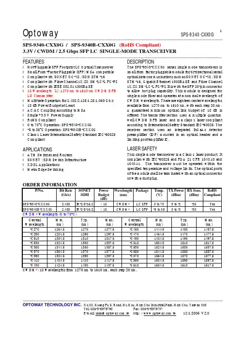
Optoway SPS-9340-CXX0G**********************************************************************************************************************************************************************************************************************************************************************************************************************************************OPTOWAY TECHNOLOGY INC. No .38, Kuang Fu S. Road, Hu Kou, Hsin Chu Industrial Park, Hsin Chu, Taiwan 303Tel: 886-3-5979798 Fax: 886-3-597973712/1/2005 V2.01SPS-9340-CXX0G / SPS-9340B-CXX0G (RoHS Compliant)3.3V / CWDM / 2.5 Gbps SFP LC SINGLE-MODE TRANSCEIVER**********************************************************************************************************************************************************************FEATURESl Hot-Pluggable SFP Footprint LC Optical Transceiver l Small Form-Factor Pluggable (SFP) MSA compatible l Compliant with SONET OC-48 / SDH STM-16l Compliant with Fibre Channel 1X/2X SM-LC-L FC-PI l Compliant with IEEE 802.3z 1000BASEl 18 Wavelength (λ): 1270 nm to 1610 nm CWDM DFB LD Transmitterl Multi-rate Operation for 2.488/2.125/1.25/1.063 Gb/s l 18 dB Power Budget at Leastl AC/AC Coupling according to MSA l Single +3.3 V Power Supply l RoHS Compliantl 0 to 70o C Operation: SPS-9340-CXX0G l -5 to 85o C Operation: SPS-9340B-CXX0Gl Class 1 Laser International Safety Standard IEC-60825 CompliantAPPLICATIONSl ATM Switches and Routersl SONET / SDH Switch Infrastructure l XDSL Applications l Metro Edge SwitchingDESCRIPTIONThe SPS-9340-CXX0G series single mode transceivers is small form factor pluggable module for bi-directional serial optical data communications such as SONET OC-48 / SDH STM-16, Gigabit Ethernet 1000BASE and Fibre Channel 1X/2X SM-LC-L FC-PI. It is with the SFP 20-pin connector to allow hot plug capability. This module is designed for single mode fiber and operates at a nominal wavelength of CWDM wavelength. There are eighteen center wavelengths available from 1270 nm to 1610 nm, with each step 20 nm. A guaranteed minimum optical link budget of 18 dB is offered The transmitter section uses a multiple quantum well CWDM DFB laser and is a class 1 laser compliant according to International Safety Standard IEC-60825. The receiver section uses an integrated InGaAs detector preamplifier (IDP) mounted in an optical header and a limiting post-amplifier IC.LASER SAFETYThis single mode transceiver is a Class 1 laser product. It complies with IEC-60825 and FDA 21 CFR 1040.10 and 1040.11. The transceiver must be operated within the specified temperature and voltage limits. The optical ports of the module shall be terminated with an optical connector or with a dust plug.ORDER INFORMATIONP/No.Bit Rate (Gb/s) SONET /SDH Power Budget (dB) Wavelength (nm) PackageTemp. (o C) TX Power (dBm) RX Sens. (dBm) RoHS Compliant SPS-9340-CXX0G 2.488 IR-2/S-16.2 > 18 CWDM * LC SFP 0 to 70 3 to -2 -20 Yes SPS-9340B-CXX0G2.488IR-2/S-16.2> 18CWDM *LC SFP-5 to 853 to -2-20YesCWDM * Wavelength (0 to 70o C) Central Wavelength Min. (nm) Typ. (nm)Max. (nm)Central WavelengthMin. (nm)Typ. (nm)Max. (nm)-C270 1264.5 1270 1277.5 -C450 1444.5 1450 1457.5 -C290 1284.5 1290 1297.5 -C470 1464.5 1470 1477.5 -C310 1304.5 1310 1317.5 -C490 1484.5 1490 1497.5 -C330 1324.5 1330 1337.5 -C510 1504.5 1510 1517.5 -C350 1344.5 1350 1357.5 -C530 1524.5 1530 1537.5 -C370 1364.5 1370 1377.5 -C550 1544.5 1550 1557.5 -C390 1384.5 1390 1397.5 -C570 1564.5 1570 1577.5 -C410 1404.5 1410 1417.5 -C590 1584.5 1590 1597.5 -C4301424.514301437.5-C6101604.516101617.5CWDM *: 18 Wavelengths from 1270 nm to 1610 nm, each step 20 nm.***********************************************************************************************************************************************************************OPTOWAY TECHNOLOGY INC. No .38, Kuang Fu S. Road, Hu Kou, Hsin Chu Industrial Park, Hsin Chu, Taiwan 303Absolute Maximum RatingsParameterSymbol Min Max Units NotesStorage TemperatureTstg -40 85 o COperating Case Temperature Topr 0 -5 70 85 o C SPS-9340-CXX0G SPS-9340B-CXX0G Power Supply VoltageVcc-0.53.6VRecommended Operating ConditionsParameterSymbol Min Typ Max Units / NotesPower Supply VoltageVcc 3.13 3.3 3.47 VOperating Case Temperature Topr 0 -5 70 85 oC / SPS-9340-CXX0G oC / SPS-9340B-CXX0GPower Supply Current I CC (TX+RX)200 300 mA Data Rate62224882670Mb/s /11. OC-48, Gigabit Ethernet and 1x/2x Fibre Channel compliant.Transmitter Specifications (0o C < Topr < 70o C, 3.13V < Vcc < 3.47V)ParameterSymbolMinTypMaxUnitsNotesOpticalOptical Transmit Power Po -2 --- 3 dBm 1Output Center Wavelength λλc –5.5 λc λc +7.5 nm 2 Output Spectrum Width ∆λ --- --- 1 nm -20 dB Width Side Mode Suppression Ratio SMSR 30 dB Extinction Ratio E R 8.2 --- --- dB Output Eye Compliant with Telecordia GR-253-GORE and ITU-T Recommendation G.957 Optical Rise Time t r 150 ps 20 % to 80% Values Optical Fall Time t f 150 ps 20 % to 80% Values Relative Intensity Noise RIN -120 dB/Hz ElectricalData Input Current – Low I IL -350 µA Data Input Current – High I IH 350 µA Differential Input Voltage V IH - V IL 0.5 2.4 V Peak-to-Peak TX Disable Input Voltage – Low T DIS, L 0 0.5 V 3 TX Disable Input Voltage – High T DIS, H 2.0 Vcc V 3 TX Disable Assert Time T ASSERT 10 µsTX Disable Deassert Time T DEASSERT 1 msTX Fault Output Voltage -- Low T FaultL 0 0.5 V 4 TX Fault Output Voltage -- High T FaultH 2.0 Vcc+0.3 V 4 1. Output power is power coupled into a 9/125 µm single mode fiber.2. ITU-T G.694.2 CWDM wavelength from 1270 nm to 1610 nm, each step 20 nm.3. There is an internal4.7K to 10K ohm pull-up resistor to VccTX.4. Open collector compatible, 4.7K to 10K ohm pull-up to Vcc (Host Supply Voltage).Receiver Specifications (0o C < Topr < 70o C, 3.1V < Vcc < 3.5V)ParameterSymbol Min Typ Max Units NotesOptical SensitivitySens -20 dBm 5,6 Maximum Input Power Pin 0 dBm 5,6Signal Detect -- Asserted Pa --- -20 dBm Transition: low to high Signal Detect -- Deasserted Pd -30 --- --- dBm Transition: high to low Signal detect -- Hysteresis 1.0 --- dBWavelength of Operation1260---1620nm***********************************************************************************************************************************************************************OPTOWAY TECHNOLOGY INC. No .38, Kuang Fu S. Road, Hu Kou, Hsin Chu Industrial Park, Hsin Chu, Taiwan 303ElectricalDifferential Output Voltage V OH – V OL 0.6 2.0 V Output LOS Voltage -- Low V OL 0 0.5 V 7 Output LOS Voltage -- HighV OH2.0Vcc+0.3V75. Measured at 223-1 PRBS at BER 1E-10.6. Measured at 27-1 PRBS at BER 1E-12 for 2.125 Gb/s, 1.25Gb/s, and 1.063 Gb/s.Module DefinitionModule DefinitionMOD-DEF2 PIN 4 MOD-DEF1 PIN 5 MOD-DEF0 PIN 6 Interpretation by Host 4SDASCLLV-TTL LowSerial module definitionprotocolModule Definition 4 specifies a serial definition protocol. For this definition, upon power up, MOD-DEF(1:2) appear as no connector (NC) and MOD-DEF(0) is TTL LOW. When the host system detects this condition, it activates the serial protocol. The protocol uses the 2-wire serial CMOS E 2PROM protocol of the ATMEL AT24C01A/02/04 family of components.*********************************************************************************************************************************************************************** OPTOWAY TECHNOLOGY INC. No.38, Kuang Fu S. Road, Hu Kou, Hsin Chu Industrial Park, Hsin Chu, Taiwan 303。