CD74AC153M96G4,CD74AC153E,CD74AC153EE4,CD74AC153M, 规格书,Datasheet 资料
- 格式:pdf
- 大小:550.51 KB
- 文档页数:14
CD54AC153, CD74AC153
DUAL 4-LINE TO 1-LINE DATA SELECTORS/MULTIPLEXERS
SCHS334A – MARCH 2003 - REVISED MAY 2003
1POST OFFICE BOX 655303 • DALLAS, TEXAS 75265DAC Types Feature 1.5-V to 5.5-V
Operation and Balanced Noise
Immunity at 30% of the Supply
DSpeed of Bipolar F, AS, and S, With
Significantly Reduced Power
Consumption
DBalanced Propagation Delays
D±24-mA Output Drive Current
– Fanout to 15 F Devices
DSCR-Latchup-Resistant CMOS Process
and Circuit Design
DExceeds 2-kV ESD Protection Per
MIL-STD-883, Method 3015
description/ordering information
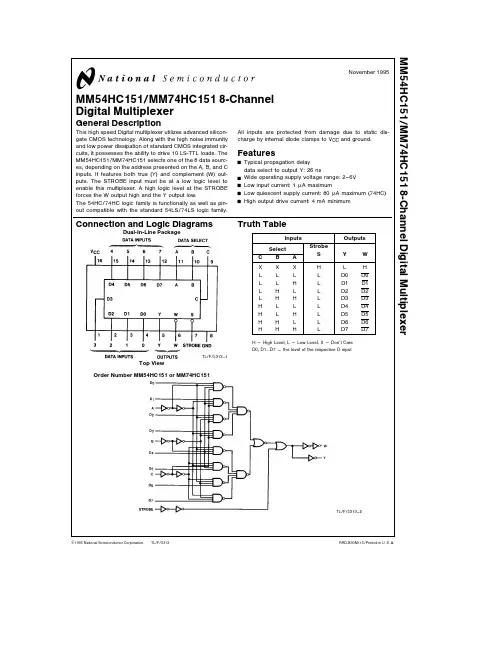
Each of these data selectors/multiplexers contains inverters and drivers to supply full binary decoding data
selection to the AND-OR gates. Separate strobe (G) inputs are provided for each of the two 4-line sections.
ORDERING INFORMATION
TAPACKAGE†ORDERABLE
PART NUMBERTOP-SIDE
MARKING
PDIP – ETubeCD74AC153ECD74AC153E
55Cto125SOICMTubeCD74AC153M–55°C to 125°CSOIC – MTape and reelCD74AC153M96AC153M
CDIP – FTubeCD54AC153F3ACD54AC153F3A
†Package drawings, standard packing quantities, thermal data, symbolization, and PCB design guidelines
are available at www.ti.com/sc/package.
FUNCTION TABLE
INPUTS
SELECT‡DATAOUTPUT
YBAC0C1C2C3G
XXXXXXHL
LLLXXXLL
LLHXXXLH
LHXLXXLL
LHXHXXLH
HLXXLXLL
HLXXHXLH
HHXXXLLL
HHXXXHLH
‡Select inputs A and B are common to both sections.
Copyright 2003, Texas Instruments IncorporatedPRODUCTION DATA information is current as of publication date.Products conform to specifications per the terms of Texas Instrumentsstandard warranty. Production processing does not necessarily includetesting of all parameters.Please be aware that an important notice concerning availability, standard warranty, and use in critical applications of
TexasInstruments semiconductor products and disclaimers thereto appears at the end of this data sheet.CD54AC153...F PACKAGE
CD74AC153...E OR M PACKAGE
(TOP VIEW)
1
2
3
4
5
6
7
816
15
14
13
12
11
10
91G
B
1C3
1C2
1C1
1C0
1Y
GNDVCC
2G
A
2C3
2C2
2C1
2C0
2Y
On products compliant to MIL-PRF-38535, all parameters are testedunlss othrwis notd. On all othr products, productionprocessing does not necessarily include testing of all parameters.
芯天下--http://oneic.com/CD54AC153, CD74AC153
DUAL 4-LINE TO 1-LINE DATA SELECTORS/MULTIPLEXERS
SCHS334A – MARCH 2003 - REVISED MAY 2003
2POST OFFICE BOX 655303 • DALLAS, TEXAS 75265logic diagram (positive logic)
TG
TGTG
TG
TGTG
TG
TGTG
TG
TGTG14
2
1
6
5
4
3
15
10
11
12
137
91GA
B
1C0
1C1
1C2
1C3
2G
2C0
2C1
2C2
2C31Y
2Y
芯天下--http://oneic.com/CD54AC153, CD74AC153
DUAL 4-LINE TO 1-LINE DATA SELECTORS/MULTIPLEXERS
SCHS334A – MARCH 2003 - REVISED MAY 2003
3POST OFFICE BOX 655303 • DALLAS, TEXAS 75265absolute maximum ratings over operating free-air temperature range†
Supply voltage range, VCC –0.5 V to 6 V. . . . . . . . . . . . . . . . . . . . . . . . . . . . . . . . . . . . . . . . . . . . . . . . . . . . . . . . . .
Input clamp current, IIK (VI < 0 or VI > VCC) (see Note 1) ±20 mA. . . . . . . . . . . . . . . . . . . . . . . . . . . . . . . . . . . .
Output clamp current, IOK (VO < 0 or VO > VCC) (see Note 1) ±50 mA. . . . . . . . . . . . . . . . . . . . . . . . . . . . . . . .
Continuous output current, IO (VO = 0 to VCC) ±50 mA. . . . . . . . . . . . . . . . . . . . . . . . . . . . . . . . . . . . . . . . . . . . . .
Continuous current through VCC or GND ±100 mA. . . . . . . . . . . . . . . . . . . . . . . . . . . . . . . . . . . . . . . . . . . . . . . . . .
Package thermal impedance, θJA (see Note 2):E package 67°C/W. . . . . . . . . . . . . . . . . . . . . . . . . . . . . . . . . . .
M package 73°C/W. . . . . . . . . . . . . . . . . . . . . . . . . . . . . . . . . .
Storage temperature range, Tstg –65°C to 150°C. . . . . . . . . . . . . . . . . . . . . . . . . . . . . . . . . . . . . . . . . . . . . . . . . . .
†Stresses beyond those listed under “absolute maximum ratings” may cause permanent damage to the device. These are stress ratings only, and
functional operation of the device at these or any other conditions beyond those indicated under “recommended operating conditions” is not
implied. Exposure to absolute-maximum-rated conditions for extended periods may affect device reliability.
NOTES:1.The input and output voltage ratings may be exceeded if the input and output current ratings are observed.
2.The package thermal impedance is calculated in accordance with JESD 51-7.
recommended operating conditions (see Note 3)
TA = 25°C–55°C to
125°C–40°C to
85°CUNIT
MINMAXMINMAXMINMAX
VCCSupply voltage1.55.51.55.51.55.5V
VCC = 1.5 V1.21.21.2
VIHHigh-level input voltageVCC = 3 V2.12.12.1V
VCC = 5.5 V3.853.853.85
VCC = 1.5 V0.30.30.3
VILLow-level input voltageVCC = 3 V0.90.90.9V
VCC = 5.5 V1.651.651.65
VIInput voltage0VCC0VCC0VCCV
VOOutput voltage0VCC0VCC0VCCV