ADF4156
- 格式:pdf
- 大小:314.13 KB
- 文档页数:24
6 GHz Fractional-N Frequency Synthesizer
ADF4156
Rev. 0 Information furnished by Analog Devices is believed to be accurate and reliable. However, no responsibility is assumed by Analog Devices for its use, nor for any infringements of patents or other rights of third parties that may result from its use. Specifications subject to change without notice. No license is granted by implication or otherwise under any patent or patent rights of Analog Devices. Trademarks and registered trademarks are the property of their respective owners. One Technology Way, P.O. Box 9106, Norwood, MA 02062-9106, U.S.A.Tel: 781.329.4700 www.analog.com Fax: 781.461.3113 ©2006 Analog Devices, Inc. All rights reserved. FEATURES
RF bandwidth to 6 GHz 2.7 V to 3.3 V power supply Separate VP allows extended tuning voltage Programmable fractional modulus Programmable charge pump currents 3-wire serial interface Digital lock detect Power-down mode Pin compatible with ADF4110/ADF4111/ADF4112/ADF4113/ADF4106/ ADF4153 and ADF4154 frequency synthesizers Programmable RF output phase Loop filter design possible with ADISimPLL Cycle slip reduction for faster lock times
APPLICATIONS
CATV equipment Base stations for mobile radio (WiMAX, GSM, PCS, DCS, SuperCell 3G, CDMA, WCDMA) Wireless handsets (GSM, PCS, DCS, CDMA, WCDMA) Wireless LANs, PMR Communications test equipment GENERAL DESCRIPTION
The ADF4156 is a 6 GHz fractional-N frequency synthesizer that implements local oscillators in the upconversion and downconversion sections of wireless receivers and transmitters. It consists of a low noise digital phase frequency detector (PFD), a precision charge pump, and a programmable reference divider. There is a sigma-delta (Σ-Δ) based fractional interpolator to allow programmable fractional-N division. The INT, FRAC, and MOD registers define an overall N divider (N = (INT + (FRAC/MOD))). The RF output phase is programmable for applications that require a particular phase relationship between the output and the reference. The ADF4156 also features cycle slip reduction circuitry leading to faster lock times without the need for modifications to the loop filter.
Control of all on-chip registers is via a simple 3-wire interface. The device operates with a power supply ranging from 2.7 V to 3.3 V and can be powered down when not in use.
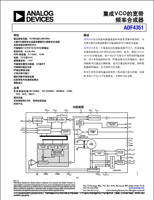
FUNCTIONAL BLOCK DIAGRAM
LOCKDETECT
NCOUNTERCP
RFCP3RFCP2RFCP4RFCP1REFERENCE
DATALE32-BITDATAREGISTERCLOCKREFINAVDD
AGNDVDD
VDDDGND
RDIVSDOUT
NDIV
DGNDCPGNDDVDDVP
CERSET
RFINARFINBOUTPUTMUXMUXOUT–+
HIGHZPHASEFREQUENCYDETECTORADF4156
THIRD ORDERFRACTIONALINTERPOLATOR
MODULUSREGFRACTIONREGINTEGERREGCURRENTSETTING×2DOUBLER5-BITRCOUNTER
CHARGEPUMP
05863-001CSR/2DIVIDER
Figure 1. ADF4156
Rev. 0 | Page 2 of 24 TABLE OF CONTENTS
Features..............................................................................................1
Applications.......................................................................................1
General Description.........................................................................1
Functional Block Diagram..............................................................1
Revision History...............................................................................2
Specifications.....................................................................................3
Timing Specifications..................................................................4
Absolute Maximum Ratings............................................................5
Thermal Impedance.....................................................................5
ESD Caution..................................................................................5
Pin Configurations and Function Descriptions...........................6
Typical Performance Characteristics.............................................7
Circuit Description...........................................................................8
Reference Input Section...............................................................8
RF Input Stage...............................................................................8
RF INT Divider.............................................................................8
INT, FRAC, MOD, and R Relationship.....................................8
RF R Counter................................................................................8
Phase Frequency Detector (PFD) and Charge Pump..............9
MUXOUT and LOCK Detect.....................................................9
Input Shift Registers.....................................................................9