PL2303 英文资料 整理
- 格式:doc
- 大小:261.00 KB
- 文档页数:9
PL-2303 USB to Serial RS232 Bridge Controller
Features
Full compliance with the USB Specification v1.1 and USB CDC v1.1
Support the RS232 Serial interface
Support automatic handshake mode
Support Remote wake-up and power management
256 bytes buffer each for upstream and downstream data flow
Support default ROM or external EEPROM for device configuration
On chip USB transceiver
On chip crystal oscillator running at 12M Hz
Supports Windows 98/SE, ME, 2000, XP, Windows CE3.0, CE .NET, Linux, and Mac OS
28 Pins SOIC package
SSOP 28 PACKAGE
(TOP VIEW)
Block Diagram
USB Port
USB
Transceiver
REGISTER/
Control USB CONFIG/
Unit SIE STATUS/
CONTROL
DOWN UP
STREAM STREAM
BUFFER BUFFER
CLOCK
SYNTHESIZE
RS-232 SERIAL
INTERFACE
OSCILLATOR EEPROM
INTERFACE
Serial Port I2C Bus
Overview
The PL-2303 operates as a bridge between one USB port and one standard RS232 Serial port. The
two large on-chip buffers accommodate data flow from two different buses. The USB bulk-type
data is adopted for maximum data transfer. Automatic handshake is supported at the Serial port.
With these, a much higher baud rate can be achieved compared to the legacy UART controller.
This device is also compliant with USB power management and remote wakeup scheme. Only
minimum power is consumed from the host during Suspend. By integrating all the function in a
SOIC-28 package, this chip is suitable for cable embedding. Users just simply hook the cable into
PC or hub’s USB port, and then they can connect to any RS-232 devices.
Pin Description
Table 1. Pins Description
Pin
No. Name Type Description
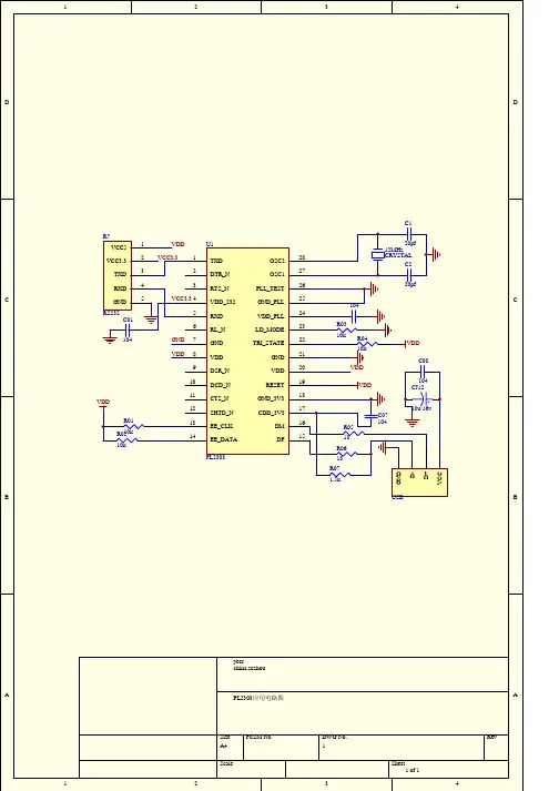
1 TXD O Data output to Serial port
2 DTR_N O Data Terminal Ready, active low
3 RTS_N O Request To Send, active low
4 VDD_232 P RS-232 VDD. The RS-232 output signals (Pin 1 ~ Pin 3) are
designed for 5V, 3.3V or 3V operation. VDD_232 should be
connected to the same power level of the RS-232 interface.
(The RS-232 input signals are always 5V~3V tolerant.)
Note: This document version only provides 5V DC characteristic
information. Refer to future revisions for updates.
5 RXD I Data input from Serial Bus
6 RI_N I Ring Indicator, active low
7 GND P Ground
8 VDD P Power
9 DSR_N I Data Set Ready, active low
10 DCD_N I Data Carrier Detect, active low
11 CTS_N I Clear To Send, active low
12 SHTD_N O Shut Down RS232 Transceiver
13 EE_CLK I/O During Reset, this pin is input for simulation purpose. During
normal operation, this pin is Serial ROM clock
14 EE_DATA I/O Serial ROM data signal
15 DP I/O USB DPLUS signal
16 DM I/O USB DMINUS signal
17 VDD_3V3 P 3.3V power for USB transceiver
18 GND_3V3 P 3.3V ground
19 RESET I System Reset
20 VDD P Power
21 GND P Ground
Type: I – Input signal O – Output signal I/O – Bi-directional signal P – Power/Ground
Supported Data Formats and Programmable Baud Rate Generator
The PL2303 USB-to-RS232 bridge controller supports versatile data formats and has a
programmable baud rate generator. The supported data formats are shown on Table 2. The
programmable baud rate generator supports baud rates up to 1.2M bps as shown in Table 3.
Table 2. Supported Data Formats
Description
Stop bits 1
1.5
2
Parity type None
Odd
Even
Mark
Space
Data bits 5, 6, 7, 8, or 16
Pin
No. Name Type Description
22 TRI_STATE I Tri-State
This pin is referred after reset.
High: RS-232 output inactive during Suspend.
Low: RS-232 output tri-state during Suspend.
23 LD_MD/
SHTD I/O Load Mode/SHTD
This pin is input during reset. Pull high with a 220K resistor to
indicate the heavy load USB device (500mA). Pull down with a
220K resistor to indicate the light load USB device 100mA).
After reset, this pin becomes output. It output the inverse of
SHTD_N.
24 VDD_PLL P 5V power for PLL
25 GND_PLL P Ground for PLL
26 PLL_TEST I PLL test mode control
27 OSC1 I Crystal oscillator input
28 OSC2 O Crystal oscillator output