
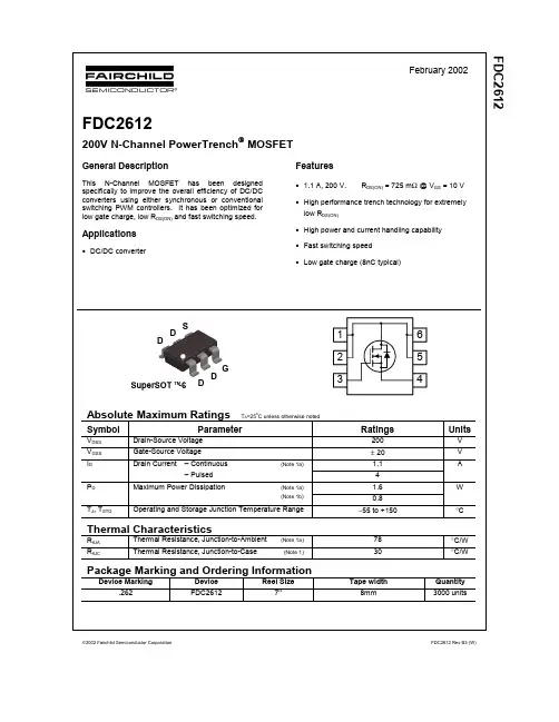
FDC2612中文资料
- 格式:pdf
- 大小:202.29 KB
- 文档页数:5


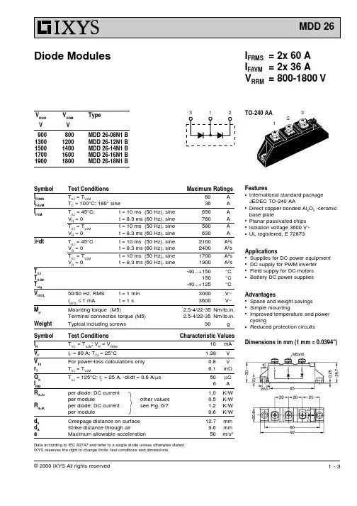
IFRMS=2x 60 AIFAVM=2x 36 AVRRM=800-1800 VVRSM VRRMTypeV V900 800MDD 26-08N1 B13001200MDD 26-12N1 B15001400MDD 26-14N1 B17001600MDD 26-16N1 B19001800MDD 26-18N1 BSymbol Test Conditions Maximum RatingsI FRMS TVJ= TVJM60AI FAVM TC= 100°C; 180° sine36AI FSM TVJ= 45°C;t = 10 ms(50 Hz), sine650A VR= 0t = 8.3 ms(60 Hz), sine760ATVJ= TVJMt = 10 ms(50 Hz), sine580A VR= 0t = 8.3 ms(60 Hz), sine630Aòi2dt TVJ = 45°C t = 10 ms(50 Hz), sine2100A2sVR= 0t = 8.3 ms(60 Hz), sine2400A2sT VJ = TVJMt = 10 ms(50 Hz), sine1700A2sVR= 0t = 8.3 ms(60 Hz), sine1900A2sT VJ -40...+150°CT VJM 150°CTstg-40...+125°CVISOL50/60 Hz, RMS t = 1 min3000V~IISOL£ 1 mA t = 1 s3600V~Md Mounting torque (M5) 2.5-4/22-35Nm/lb.in. Terminal connection torque (M5) 2.5-4/22-35Nm/lb.in.Weight Typical including screws90g Symbol Test Conditions Characteristic ValuesI R TVJ= TVJM; VR= VRRM10mAVF IF= 80 A; TVJ= 25°C 1.38VVT0For power-loss calculations only0.8Vr T TVJ= TVJM6.1m WQS TVJ= 125°C; IF= 25 A, -di/dt = 0.6 A/m s50m CIRM6ARthJC per diode; DC current 1.0K/W per module other values0.5K/WRthJK per diode; DC current see Fig. 6/7 1.2K/W per module0.6K/Wd S Creepage distance on surface12.7mmd A Strike distance through air9.6mma Maximum allowable acceleration50m/s2Featuresq International standard package JEDEC TO-240 AAq Direct copper bonded Al2O3 -ceramic base plateq Planar passivated chipsq Isolation voltage 3600 V~q UL registered, E 72873 Applicationsq Supplies for DC power equipmentq DC supply for PWM inverterq Field supply for DC motorsq Battery DC power supplies Advantagesq Space and weight savingsq Simple mountingq Improved temperature and power cyclingq Reduced protection circuits Dimensions in mm (1 mm = 0.0394")Diode ModulesTO-240 AA123Data according to IEC 60747 and refer to a single diode unless otherwise stated.IXYS reserves the right to change limits, test conditions and dimensions元器件交易网Fig. 1Surge overload currentI FSM : Crest value, t: durationFig. 2òi2dt versus time (1-10 ms)Fig. 2a Maximum forward currentat case temperatureFig. 3Power dissipation versusforward current and ambienttemperature (per diode)Fig. 4Single phase rectifier bridge:Power dissipation versus directoutput current and ambienttemperatureR= resistive loadL= inductive loadFig. 5Three phase rectifier bridge:Power dissipation versus direct output current and ambient temperatureFig. 6Transient thermal impedancejunction to case (per diode)Fig. 7Transient thermal impedancejunction to heatsink (per diode)R thJK for various conduction angles d: d R thJK (K/W) DC 1.20180° 1.22120° 1.2460° 1.2730°1.30Constants for Z thJK calculation:i R thi (K/W)t i (s)10.010.001220.030.09530.960.45540.20.495R thJC for various conduction angles d: d R thJC (K/W) DC 1.00180° 1.02120° 1.0460° 1.0730°1.10Constants for Z thJC calculation:i R thi (K/W)t i (s)10.010.001220.030.09530.960.455。