
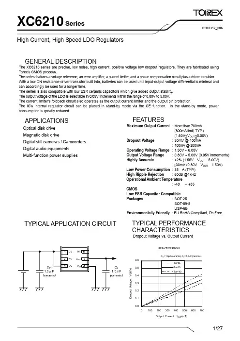
XC6210
- 格式:pdf
- 大小:462.74 KB
- 文档页数:27
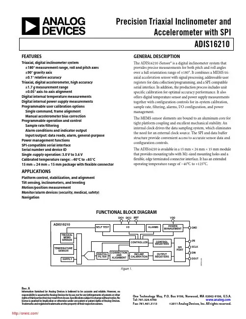
Precision Triaxial Inclinometer andAccelerometer with SPIADIS16210Rev. AInformation furnished by Analog Devices is believed to be accurate and reliable. However , no responsibility is assumed by Analog Devices for its use, nor for any infringements of patents or other rights of third parties that may result from its use. Specifications subject to change without notice. No license is granted by implication or otherwise under any patent or patent rights of Analog Devices. T rademarks and registered trademarks are the property of their respective owners.One Technology Way, P.O. Box 9106, Norwood, MA 02062-9106, U.S.A.Tel: 781.329.4700 Fax: 781.461.3113 ©2011 Analog Devices, Inc. All rights reserved.FEATURESTriaxial, digital inclinometer system±180° measurement range, roll and pitch axes ±90° gravity axis±0.1° relative accuracyTriaxial, digital accelerometer, high accuracy ±1.7 g measurement range ±0.05° axis-to-axis alignmentDigital internal temperature measurements Digital internal power supply measurements Programmable user calibration options Single command, frame alignment Manual accelerometer bias correction Programmable operation and control Sample rate/filteringAlarm conditions and indicator outputInput/output: data ready, alarm, general-purpose Power management functions SPI-compatible serial interface Serial number and device IDSingle-supply operation: 3.0 V to 3.6 VCalibrated temperature range: −40°C to +85°C15 mm × 24 mm × 15 mm package with flexible connectorAPPLICATIONSPlatform control, stabilization, and alignment Tilt sensing, inclinometers, and leveling Motion/position measurementMonitor/alarm devices (security, medical, safety) NavigationGENERAL DESCRIPTIONThe ADIS16210 i Sensor® is a digital inclinometer system that provides precise measurements for both pitch and roll angles over a full orientation range of ±180°. It combines a MEMS tri-axial acceleration sensor with signal processing, addressable user registers for data collection/programming, and a SPI-compatible serial interface. In addition, the production process includes unit specific calibration for optimal accuracy performance. It also offers digital temperature sensor and power supply measurements together with configuration controls for in-system calibration, sample rate, filtering, alarms, I/O configuration, and power management.The MEMS sensor elements are bound to an aluminum core for tight platform coupling and excellent mechanical stability. An internal clock drives the data sampling system, which eliminates the need for an external clock source. The SPI and data buffer structure provide convenient access to accurate sensor data and configuration controls.The ADIS16210 is available in a 15 mm × 24 mm × 15 mm module that provides mounting tabs with M2-sized mounting holes and a flexible, edge terminated connector interface. It has an extended operating temperature range of −40°C to +125°C.FUNCTIONAL BLOCK DIAGRAM09593-001Figure 1.ADIS16210Rev. A | Page 2 of 20TABLE OF CONTENTSFeatures..............................................................................................1 Applications.......................................................................................1 General Description.........................................................................1 Functional Block Diagram..............................................................1 Revision History...............................................................................2 Specifications.....................................................................................3 Timing Specifications..................................................................4 Absolute Maximum Ratings............................................................5 ESD Caution..................................................................................5 Pin Configuration and Function Descriptions.............................6 Basic Operation.................................................................................7 Reading Sensor Data....................................................................7 Device Configuration..................................................................7 User Register Map............................................................................8 Sensor Data........................................................................................9 Output Data Registers..................................................................9 Signal Processing, Bias Correction, and Alignment..................12 System Tools....................................................................................14 Global Commands.....................................................................14 Input/Output Functions............................................................14 Device Identification..................................................................15 Status/Error Flags.......................................................................15 Flash Memory Management.....................................................15 Alarms..............................................................................................16 System Alarm..............................................................................16 Static Alarms...............................................................................16 Dynamic Alarms........................................................................16 Alarm Reporting........................................................................16 Applications Information..............................................................17 Interface Board...........................................................................17 Mating Connector......................................................................17 Outline Dimensions.......................................................................18 Ordering Guide.. (18)REVISION HISTORY6/11—Rev. 0 to Rev. AChanges to Table 1............................................................................3 Changes to Table 23........................................................................12 Changes to Figure 24 and Figure 25 (17)4/11—Revision 0: Initial VersionADIS16210SPECIFICATIONST A = −40°C to +85°C, VDD = 3.0 V to 3.6 V, unless otherwise noted.1 The digital I/O signals are 5 V tolerant.2 Endurance is qualified as per JEDEC Standard 22, Method A117, and measured at −40°C, +25°C, +85°C, and +125°C.3 Retention lifetime equivalent at junction temperature (T J) = 85°C as per JEDEC Standard 22, Method A117. Retention lifetime decreases with junction temperature. See Figure 22.4 The start-up times presented do not include the data capture time, which is dependent on the AVG_CNT register settings.5 The RST pin must be held low for at least 15 ns.Rev. A | Page 3 of 20ADIS16210Rev. A | Page 4 of 20TIMING SPECIFICATIONST A = 25°C, VDD = 3.3 V , unless otherwise noted.1Guaranteed by design, not tested.Timing DiagramsCSSCLKDOUTDIN09593-002Figure 2. SPI Timing and SequenceSCLKt STALL09593-003Figure 3. DIN Bit SequenceADIS16210Rev. A | Page 5 of 20ABSOLUTE MAXIMUM RATINGSTable 3.Parameter Rating Acceleration Any Axis, Unpowered 3500 g Any Axis, Powered 3500 gVDD to GND −0.3 V to +6.0 VDigital Input Voltage to GND −0.3 V to +5.3 V Digital Output Voltage to GND −0.3 V to VDD + 0.3 V Analog Inputs to GND −0.3 V to +3.6 V Operating Temperature Range −40°C to +125°CStorage Temperature Range −65°C to +150°CStresses above those listed under Absolute Maximum Ratings may cause permanent damage to the device. This is a stress rating only; functional operation of the device at these or any other conditions above those indicated in the operationalsection of this specification is not implied. Exposure to absolute maximum rating conditions for extended periods may affect device reliability. Table 4. Package CharacteristicsPackage TypeθJA θJC Device Weight 15-Lead Module 31°C/W11°C/W 7.2 gramsESD CAUTIONADIS16210Rev. A | Page 6 of 20PIN CONFIGURATION AND FUNCTION DESCRIPTIONS09593-004BOTTOM VIEWNOTES1. LEADS ARE EXPOSED COPPER PADS LOCATED ON THE BOTTOM SIDE OF THE FLEXIBLE INTERFACE CABLE.2. PACKAGE IS NOT SUITABLE FOR SOLDER REFLOW ASSEMBLY PROCESSES.3. EXAMPLE MATING CONNECTOR:AVX CORPORATIONFLAT FLEXIBLE CONNECTOR (FFC)P/N: 04-6288-015-000-846.Figure 4. Pin Configuration1S is supply, O is output, I is input, and I/O is input/output.ADIS16210Rev. A | Page 7 of 20BASIC OPERATIONThe ADIS16210 is an autonomous system that requires no user initialization. Upon receiving a valid power supply, it initializes itself and starts sampling, processing, and loading data into the output registers. When using the factory default configuration, DIO1 provides a data ready signal. The SPI interface enables simple integration with many embedded processor platforms, as shown in Figure 5 (electrical connection) and Table 6 (processor pin descriptions).I/O LINES ARE COMPATIBLE WITH09593-006Figure 5. Electrical Connection DiagramThe ADIS16210 SPI interface supports full duplex serial commu-nication (simultaneous transmit and receive) and uses the bit sequence shown in Figure 9. Table 7 provides a list of the most common settings that initialize the serial port of a processor for the ADIS16210 SPI interface.Table 7. Generic Master Processor SPI SettingsProcessor Setting DescriptionMasterADIS16210 operates as a slave SCLK Rate ≤ 830 kHz Maximum serial clock rateSPI Mode 3 CPOL = 1 (polarity), CPHA = 1 (phase) MSB-First Mode Bit sequence16-Bit ModeShift register/data lengthREADING SENSOR DATAA single register read requires two 16-bit SPI cycles. The first cycle requests the contents of a register using the bit assignments in Figure 9. The register contents then follow on DOUT, during the second sequence.Figure 6 includes three single register reads in succession. In this example, the process starts with DIN = 0x0400 to request the contents of the XACCL_OUT register, followed by 0x0600 to request the contents of the Y ACCL_OUT register, and then 0x0800 to request the contents of the ZACCL_OUT register. Full duplex operation enables processors to use the same 16-bit SPI cycle to read data from DOUT while requesting the next set of data on DIN.DIN DOUT09593-007Figure 6. SPI Read Example RemoveFigure 7 provides an example of four SPI signals when reading PROD_ID in a repeating pattern.DOUT = 0011 1111 0101 1100 = 0x3F52 = 16210DIN = 0101 0110 0000 0000 = 0x5600CS SCLK DIN DOUT09593-008Figure 7. SPI Read Example, Second 16-Bit SequenceDEVICE CONFIGURATIONThe user register map (Table 8) provides a variety of control registers, which enable optimization for specific applications. The SPI provides access to these registers, one byte at a time, using the bit assignments shown in Figure 9. Each register has 16 bits, where Bits[7:0] represent the lower address and Bits[15:8] represent the upper address. Figure 8 displays the SPI signal pattern for writing 0x07 to Address 0x38, which sets the number of averages to 128 and the sample rate to 4 SPS.DIN = 1011 1000 0000 0111 = 0xB807, SET AVG_CNT[7:0] = 0x07CS SCLKDIN09593-009Figure 8. Example SPI Write Pattern09593-113R/W R/W A6A5A4A3A2A1A0DC7DC6DC5DC4DC3DC2DC1DC0D0D1D2D3D4D5D6D7D8D9D10D11D12D13D14D15CS SCLK DIN DOUTA6A5D13D14D15NOTES1.DOUT BITS ARE PRODUCED ONLY WHEN THE PREVIOUS 16-BIT DIN SEQUENCE STARTS WITH R/W = 0.2.WHEN CS IS HIGH, DOUT IS IN A THREE-STATE, HIGH IMPEDANCE MODE, WHICH ALLOWS MULTIFUNCTIONAL USE OF THE LINE FOR OTHER DEVICES.Figure 9. SPI Communication Bit SequenceADIS16210Rev. A | Page 8 of 20USER REGISTER MAPFigure 10 provides a diagram of the dual memory structure used to manage operation and store user settings. Writing con-figuration data to a control register updates its SRAM contents, which are volatile.Most of the user registers have mirror locations in flash memory (see Table 8, for “yes” in the Flash Backup column). Use the manual flash backup command in GLOB_CMD[6] (DIN =0xBE40) to save these settings into the nonvolatile flash memory. The flash backup process requires a valid power supply level and zero SPI communication for the entire 28 ms process time.09593-116Table 8. User Register Memory Map 1Name R/W Flash Backup Address Size (Bytes) Function Reference FLASH_CNT R Yes 0x00 2 Diagnostics, flash write counter (16-bit binary) Table 37 SUPPLY_OUT R No 0x02 2 Output, power supply Table 20 XACCL_OUT R No 0x04 2 Output, x-axis acceleration Table 9 YACCL_OUT R No 0x06 2 Output, y-axis acceleration Table 10 ZACCL_OUT R No 0x08 2 Output, z-axis acceleration Table 11 TEMP_OUT R No 0x0A 2 Output, internal temperature Table 18 X I NCL_OUT R No 0x0C 2 Output, ±180° x-axis inclination Table 13 Y I NCL_OUT R No 0x0E 2 Output, ±180° y-axis inclination Table 14 Z I NCL_OUT R No 0x10 2 Output, ±180° z-axis inclination Table 15 XACCL_NULL R/W Yes 0x12 2 Calibration, x-axis acceleration offset null Table 24 YACCL_NULL R/W Yes 0x14 2 Calibration, y-axis acceleration offset null Table 25 ZACCL_NULL R/W Yes 0x16 2 Calibration, z-axis acceleration offset null Table 26 0x18 to 0x1F 8 Reserved, do not write to these locationsALM_MAG_X R/W Yes 0x20 2 Alarm, x-axis amplitude threshold Table 39 ALM_MAG_Y R/W Yes 0x22 2 Alarm, y-axis amplitude threshold Table 40 ALM_MAG_Z R/W Yes 0x24 2 Alarm, z-axis amplitude threshold Table 41 ALM_MAG_S R/W Yes 0x26 2 Alarm, system alarm threshold Table 42 ALM_SMPL_X R/W Yes 0x28 2 Alarm, x-axis sample period Table 43 ALM_SMPL_Y R/W Yes 0x2A 2 Alarm, y-axis sample period Table 44 ALM_SMPL_Z R/W Yes 0x2C 2 Alarm, z-axis sample period Table 45 ALM_CTRL R/W Yes 0x2E 2 Operation, alarm control Table 380x30 2 Reserved GPIO_CTRL R/W Yes 0x32 2 Operation, general I/O configuration and data Table 31 MSC_CTRL R/W Yes 0x34 2 Operation, orientation mode Table 27 DIO_CTRL R/W Yes 0x36 2 Operation, digital I/O configuration and data Table 30 AVG_CNT R/W Yes 0x38 2 Operation, decimation filter configuration Table 22 SLP_CNT R/W Yes 0x3A 2 Operation, sleep count Table 29 D I AG_STAT R No 0x3C 2 Diagnostics, system status register Table 36 GLOB_CMD W No 0x3E 2 Operation, system command register Table 28 0x40 to 0x51 16 ReservedLOT_ID1 R N/A 0x52 2 Lot identification, Code 1 Table 32 LOT_ID2 R N/A 0x54 2 Lot identification, Code 2 Table 33 PROD_ID R N/A 0x56 2 Production identification number Table 34 SER I AL_NUM R N/A 0x58 2 Serial numberTable 351N/A means not applicable.ADIS16210Rev. A | Page 9 of 20SENSOR DATAOUTPUT DATA REGISTERSThe ADIS16210 provides a set of output registers for three orthogonal axes of acceleration: incline angles, internal temperature, and power supply.AccelerometersThe accelerometers respond to both static (gravity) and dynamic acceleration using the polarity shown in Figure 11. XACCL_OUT (Table 9), Y ACCL_OUT (Table 10), and ZACCL_OUT (Table 11) provide user access to digital calibrated accelerometer data for each axis. For example, use DIN = 0x0400 to request the x-axis data (XACCL_OUT). After reading the contents of one of these registers, convert the 16-bit, twos complement number into a decimal equivalent, and then divide that number by 16,384 to convert the measurement into units of gravity (g ). Table 12 provides several examples of this data format.Table 9. XACCL_OUT (Base Address = 0x04), Read OnlyBits Description [15:0] X-axis accelerometer output data, twos complement,1 LSB = 1 g ÷ 16,384 = ~61 μg /LSB, 0 g = 0x0000Table 10. YACCL_OUT (Base Address = 0x06), Read OnlyBits Description [15:0] Y-axis accelerometer output data, twos complement,1 LSB = 1 g ÷ 16,384 = ~61 μg /LSB, 0 g = 0x0000Table 11. ZACCL_OUT (Base Address = 0x08), Read OnlyBits Description [15:0] Z-axis accelerometer output data, twos complement,1 LSB = 1 g ÷ 16,384 = ~61 μg /LSB, 0 g = 0x0000Table 12. Accelerometer Data Format ExamplesOrientation (g ) Decimal HexBinary+1.7 +27,853 0x6CCD 0110 1100 1100 1101 +1 +16,384 0x4000 0100 0000 0000 0000 +2/16,384 +2 0x0002 0000 0000 0000 0010 +1/16,384 +1 0x0001 0000 0000 0000 0001 0 0 0x0000 0000 0000 0000 0000 −1/16,384 −1 0xFFFF 1111 1111 1111 1111 −2/16,384 −2 0xFFFE 1111 1111 1111 1110 −1 −16,384 0xC000 1100 0000 0000 0000 −1.7 −27,8530x93331001 0011 0011 0011InclinometersRegisters XINCL_OUT (Table 13), YINCL_OUT (Table 14), and ZINCL_OUT (Table 15) provide access to incline angle data for each axis. For example, set DIN = 0x0E00 to request y-axis data (YINCL_OUT). Use the following process to translate the contents of these registers into degrees (°): 1. Convert the 16-bit, twos complement number into adecimal equivalent.2. Multiply the decimal equivalent by 180.3. Divide the result of Step 2 by 32,768.Table 16 provides several examples of this data format. Table 13. XINCL_OUT (Base Address = 0x0C), Read OnlyBits Description [15:0] X-axis inclinometer output data, binary,0° = 0x0000, 1 LSB = 180°/32,768 = ~0.0055°/LSBTable 14. YINCL_OUT (Base Address = 0x0E), Read OnlyBits Description [15:0] Y-axis inclinometer output data, binary,0° = 0x0000, 1 LSB = 180°/32,768 = ~0.055°/LSBTable 15. ZINCL_OUT (Base Address = 0x10), Read OnlyBits Description [15:0] Z-axis inclinometer output data, binary,0° = 0x0000, 1 LSB = 180°/32,768 = ~0.0055°/LSBTable 16. Incline Angle Data Format ExamplesOrientation Decimal Hex Binary+179.9945° +32,767 0x7FFF 0111 1111 1111 1111 +0.011° +2 0x0002 0000 0000 0000 0010 +0.0055° +1 0x0001 0000 0000 0000 0001 0° 0 0x0000 0000 0000 0000 0000 −0.0055° −1 0xFFFF 1111 1111 1111 1111 −0.011° −2 0xFFFE 1111 1111 1111 1110 −180° −32,768 0x80001000 0000 0000 0000Figure 11 through Figure 16 provide orientation examples and the associated output values for each accelerometer and incli-nometer register. These examples assume the factory default configuration for the gravity vector (z-axis, pointed up). See the MSC_CTRL (Table 27) for additional options for gravity vector definitions.ADIS16210Rev. A | Page 10 of 20Figure 11. Inclinometer Output Example, 0° Tilt09593-013a Za Ya XFigure 12. Inclinometer Output Example, −30° Y-Axis Tilt09593-016a Za Ya XFigure 13. Inclinometer Output Exampls, −30° X-Axis Tilt09593-014aXa Y a ZFigure 14. Inclinometer Output Example, +30° Y-Axis Tilt09593-017a Xa Ya ZFigure 15. Inclinometer Output Example, +30° X-Axis Tilt09593-015a Xa Za YFigure 16. Inclinometer Output Example, 180° TiltTable 17. Orientation/Output Examples for Z-Axis Gravity Orientation 1Register Figure 11 Figure 12 Figure 13 Figure 14 Figure 15 Figure 16 XACCL_OUT 0 0 −8192 0 +8192 0 YACCL_OUT 0 −8192 0 +8192 0 0ZACCL_OUT +16,384 +14,189 +14,189 +14,189 +14,189 −16,384 X NCL_OUT 0 0 −5462 0 +5462 −32,768 Y NCL_OUT 0 −5462 0 +5462 0 −32,768Z I NCL_OUT +16,384 +10,922 +10,922 +10,922 +10,922 −16,3841Register setting for Z-axis gravity orientation is MSC_CTRL[7:0] = xxxx xx10.分销商库存信息:ANALOG-DEVICESADIS16210CMLZ ADIS16210/PCBZ。
硬件经典面试 100 题(附参考答案)1 、请列举您知道的电阻、电容、电感品牌(最好包括国内、国外品牌) 。
电阻:美国:AVX VISHAY 威世日本:KOA 兴亚、Kyocera 京瓷、muRata 村田、Panasonic 松下、ROHM 罗姆、 susumu 、TDK台湾:LIZ 丽智、PH YCO 飞元、RALEC 旺诠、ROYALOH M 生、SUP EROH 美隆、 TA -I 大毅、TMTEC 泰铭、TOKEN德键、TYOHM 幸亚、Uni Ohm 厚声、VITROHMVIKING 光颉、WALSIN 华新科、YAGEO 国巨 新加坡: ASJ 中国 电容 美国 英国 日本Matsushita 松下、 muRata 村田、 NEC 、 nichicon (蓝宝石)尼吉康、NipponChemi-Con (黑金刚、嘉美工)日本化工、 Panasonic 松下、Raycon 威康、Rubycon (红 宝石)、SANYOE 洋、TAIYO YUDENt 诱、TDK TK 东信 韩国:SAMSUNGS 星、SAMWHE 和、SAMYOUNB 莹 台湾:CAPSUNJCAPXON 丰宾)凯普松、Chocon Choyo ELITE 金山、EVERCON EYANG 宇阳、GEMCO 至美、GSC 杰商、G-Luxon 世昕、HEC 禾伸堂、HERME 合美电机、JACKCO 融欣、JPCON 正邦、LELO N 立隆、LTEC 辉城、OST奥斯特、SACON 士康、SUSCO冠佐、TAICO N 台康、TEA PO 智宝、WALSIN 华 新科、 香港: 电子、 风华、 山三水日明电子、Rukyco n 海丰三力、San con 海门三鑫、SEACONS 圳鑫龙茂电子、SHENGD 扬州升达、TAI-TECH 台 庆、TF 南通同飞、TEAMYOUNG 扬、 QIFA 奇发电子 电感: 美国: 德国: 日本: 太诱、 台湾:WALSIN 华新科、 巨中国: Gausstek 紫泰荆、肇庆英达FH 风华、捷比信AVX KEMET 基美、Skywell 泽天、VISHA 丫威世NOVER 若华德国:EPCOSWIMA 威马丹麦:JENSEN 战木申ELNA 伊娜、FUJITSU 富士通、HITACHI 日立、KOA 兴亚、Kyocera 京瓷、YAGEC 国巨FUJICO N 富之光、SAMXO 万裕 中国:AiSHi 艾华科技、Cha ng 常州华威FCON 深圳金富康、FH 广东HEC 东阳光、JIANGHAI 南通江海、JICON 吉光电子、LM 佛山利明、 佛 AEM 、 AVX 、 Coilcraft 线艺、 Pulse 普思、 VISHAY 威世EPCO 、S WEKOA 兴亚、muRata 村田、Panasonic 松下、sumida 胜美达、TAIYOYUDEN TDK TOKO TOREX 特瑞仕CHILISIN 奇力新、美磊、TAI -TECH 台庆、TOKEN 德键、VIKING 光颉、YAGEC H丰晶、GLE 格莱尔、FH 风华、CODACA^达嘉、Sun lord 顺络、2、请解释电阻、电容、电感封装的含义: 表示的是尺寸参数。

硬件经典面试 100 题(附参照答案)1、请列举您知道的电阻、电容、电感品牌(最好包含国内、外国品牌)。
电阻:美国: AVX、 VISHAY威世日本: KOA 兴亚、 Kyocera 京瓷、 muRata 村田、 Panasonic 松下、 ROHM 罗姆、susumu、TDK台湾: LIZ 丽智、PHYCOM 飞元、RALEC旺诠、ROYALOHM厚生、SUPEROHM美隆、 TA-I 大毅、 TMTEC 泰铭、 TOKEN德键、 TYOHM 幸亚、 UniOhm 厚声、 VITROHM、VIKING 光颉、 WALSIN 华新科、YAGEO国巨新加坡: ASJ中国: FH 风华、捷比信电容:美国: AVX、 KEMET 基美、 Skywell 泽天、 VISHAY威世英国: NOVER 诺华德国: EPCOS、 WIMA 威马丹麦: JENSEN战神日本: ELNA 伊娜、 FUJITSU富士通、 HITACHI 日立、 KOA 兴亚、 Kyocera 京瓷、Matsushita 松下、 muRata 村田、 NEC、nichicon(蓝宝石)尼吉康、 Nippon Chemi-Con(黑金刚、嘉美工)日本化工、Panasonic 松下、 Raycon 威康、 Rubycon(红宝石)、SANYO三洋、 TAIYO YUDEN太诱、 TDK、TK 东信韩国: SAMSUNG 三星、 SAMWHA 三和、 SAMYOUNG三莹台湾:CAPSUN、CAPXON(丰宾)凯普松、Chocon、Choyo、ELITE 金山、EVERCON、 EYANG 宇阳、 GEMCON 至美、GSC 杰商、G-Luxon 世昕、HEC 禾伸堂、HERMEI 合美电机、JACKCON融欣、JPCON正邦、 LELON 立隆、 LTEC辉城、OST 奥斯特、SACON 士康、SUSCON冠佐、TAICON 台康、TEAPO 智宝、WALSIN华新科、 YAGEO国巨香港: FUJICON 富之光、 SAMXON 万裕中国: AiSHi 艾华科技、 Chang 常州华威电子、 FCON 深圳金富康、 FH 广东风华、 HEC 东阳光、 JIANGHAI 南通江海、 JICON 吉光电子、 LM 佛山利明、佛山三水日明电子、 Rukycon 海丰三力、Sancon 海门三鑫、 SEACON深圳鑫龙茂电子、 SHENGDA扬州升达、 TAI-TECH台庆、 TF 南通同飞、 TEAMYOUNG天扬、 QIFA 奇发电子电感:美国: AEM、AVX、Coilcraft 线艺、 Pulse 普思、 VISHAY 威世德国: EPCOS、WE日本:KOA 兴亚、muRata 村田、Panasonic 松下、sumida 胜美达、 TAIYO YUDEN 太诱、 TDK、 TOKO、TOREX特瑞仕台湾: CHILISIN 奇力新、美磊、 TAI-TECH台庆、 TOKEN 德键、 VIKING 光颉、WALSIN 华新科、 YAGEO国巨中国: Gausstek 丰晶、GLE 格莱尔、 FH 风华、 CODACA科达嘉、 Sunlord 顺络、紫泰荆、肇庆英达2、请解说电阻、电容、电感封装的含义:0402、 0603、 0805。

Document Number: 81352For technical questions, contact: emittertechsupport@High Speed Infrared Emitting Diode, RoHS Compliant, 870 nm,GaAlAs Double HeteroTSFF6210Vishay SemiconductorsDESCRIPTIONTSFF6210 is an infrared, 870 nm emitting diode in GaAlAs double hetero (DH) technology with high radiant power and high speed, molded in a clear, untinted plastic package.FEATURES•Package type: leaded •Package form: T-1¾•Dimensions (in mm): ∅ 5•Peak wavelength: λp = 870 nm •High reliability •High radiant power •High radiant intensity•Angle of half intensity: ϕ = ± 10°•Low forward voltage•Suitable for high pulse current operation •High modulation bandwidth: f c = 24 MHz•Good spectral matching with Si photodetectors•Lead (Pb)-free component in accordance with RoHS 2002/95/EC and WEEE 2002/96/ECAPPLICATIONS•Infrared video data transmission between Camcorder and TV set•Free air data transmission systems with high modulation frequencies or high data transmission rate requirements •Smoke-automatic fire detectorsNoteTest conditions see table “Basic Characteristics”NoteMOQ: minimum order quantity94 8389PRODUCT SUMMARYCOMPONENT I e (mW/sr)ϕ (deg)λP (nm)t r (ns)TSFF6210180± 1087015ORDERING INFORMATIONORDERING CODE PACKAGINGREMARKSPACKAGE FORMTSFF6210BulkMOQ: 4000 pcs, 4000 pcs/bulkT-1¾ABSOLUTE MAXIMUM RATINGSPARAMETER TEST CONDITIONSYMBOLVALUE UNIT Reverse voltage V R 5V Forward current I F 100mA Peak forward current t p /T = 0.5, t p = 100 µsI FM 200mA Surge forward current t p = 100 µs I FSM 1A Power dissipationP V180mW For technical questions, contact: emittertechsupport@Document Number: 81352TSFF6210Vishay Semiconductors High Speed Infrared Emitting Diode, RoHSCompliant, 870 nm, GaAlAs Double HeteroNoteT amb = 25 °C, unless otherwise specifiedFig. 1 - Power Dissipation Limit vs. Ambient Temperature Fig. 2 - Forward Current Limit vs. Ambient TemperatureNoteT amb = 25 °C, unless otherwise specifiedJunction temperature T j 100°C Operating temperature range T amb - 40 to + 85°C Storage temperature range T stg - 40 to + 100°C Soldering temperaturet ≤ 5 s, 2 mm from case T sd 260°C Thermal resistance junction/ambient J-STD-051, leads 7 mm,soldered on PCB R thJA230K/WABSOLUTE MAXIMUM RATINGSPARAMETER TEST CONDITIONSYMBOLVALUEUNITBASIC CHARACTERISTICSPARAMETER TEST CONDITION SYMBOLMIN.TYP.MAX.UNIT Forward voltageI F = 100 mA, t p = 20 ms V F 1.5 1.8V I F = 1 A, t p = 100 µsV F 2.3 3.0V Temperature coefficient of V F I F = 1 mA TK VF - 1.8mV/K Reverse current V R = 5 VI R 10µA Junction capacitance V R = 0 V, f = 1 MHz, E = 0C j 125pF Radiant intensity I F = 100 mA, t p = 20 ms I e 90180450mW/sr I F = 1 A, t p = 100 µs I e 1800mW/sr Radiant powerI F = 100 mA, t p = 20 msφe 50mW Temperature coefficient of φe I F = 100 mATK φe - 0.35%/K Angle of half intensity ϕ± 10deg Peak wavelength I F = 100 mA λp 870nm Spectral bandwidthI F = 100 mA Δλ40nm Temperature coefficient of λp I F = 100 mA TK λp 0.25nm/K Rise time I F = 100 mA t r 15ns Fall time I F = 100 mAt f 15ns Cut-off frequency I DC = 70 mA, I AC = 30 mA ppf c 24MHz Virtual source diameterd3.7mmTSFF6210High Speed Infrared Emitting Diode, RoHSCompliant, 870 nm, GaAlAs Double HeteroVishay SemiconductorsBASIC CHARACTERISTICST amb = 25°C, unless otherwise specifiedFig. 3 - Pulse Forward Current vs. Pulse Duration Fig. 4 - Forward Current vs. Forward Voltage Fig. 5 - Radiant Intensity vs. Forward CurrentFig. 6 - Relative Radiant Power vs. Wavelength Fig. 7 - Relative Radiant Intensity vs. Angular Displacement Fig. 8 - Attenuation vs. FrequencyDocument Number: 81352For technical questions, contact: emittertechsupport@ TSFF6210Vishay Semiconductors High Speed Infrared Emitting Diode, RoHSCompliant, 870 nm, GaAlAs Double Heteroin millimetersPACKAGE DIMENSIONS For technical questions, contact: emittertechsupport@ Document Number: 81352Disclaimer Legal Disclaimer NoticeVishayAll product specifications and data are subject to change without notice.Vishay Intertechnology, Inc., its affiliates, agents, and employees, and all persons acting on its or their behalf (collectively, “Vishay”), disclaim any and all liability for any errors, inaccuracies or incompleteness contained herein or in any other disclosure relating to any product.Vishay disclaims any and all liability arising out of the use or application of any product described herein or of any information provided herein to the maximum extent permitted by law. The product specifications do not expand or otherwise modify Vishay’s terms and conditions of purchase, including but not limited to the warranty expressed therein, which apply to these products.No license, express or implied, by estoppel or otherwise, to any intellectual property rights is granted by this document or by any conduct of Vishay.The products shown herein are not designed for use in medical, life-saving, or life-sustaining applications unless otherwise expressly indicated. Customers using or selling Vishay products not expressly indicated for use in such applications do so entirely at their own risk and agree to fully indemnify Vishay for any damages arising or resulting from such use or sale. Please contact authorized Vishay personnel to obtain written terms and conditions regarding products designed for such applications.Product names and markings noted herein may be trademarks of their respective owners.元器件交易网Document Number: 。