5082-A511-HH300中文资料
- 格式:pdf
- 大小:196.94 KB
- 文档页数:14
Devices
AlGaAsOrangeRedHERGreenPackageHDSP-HDSP-HDSP-HDSP- DescriptionDrawing
A411A111A211A5117.6 mm Common Anode Right Hand DecimalA
A413A113A213A5137.6 mm Common Cathode Right Hand DecimalB
F411F111F211F51110 mm Common Anode Right Hand DecimalC
F413F113F213F51310 mm Common Cathode Right Hand DecimalD
G411G111G211G51110 mm Two Digit Common Anode Right Hand DecimalE
G413G113G213G51310 mm Two Digit Common Cathode Right Hand DecimalF
H411H111H211H51114.2 mm Common Anode Right Hand DecimalG
H413H113H213H51314.2 mm Common Cathode Right Hand DecimalH
K411K111K211K51114.2 mm Two Digit Common Anode Right Hand DecimalI
K413K113K213K51314.2 mm Two Digit Common Cathode Right Hand DecimalJBlack Surface Seven Segment
Displays
Technical Data
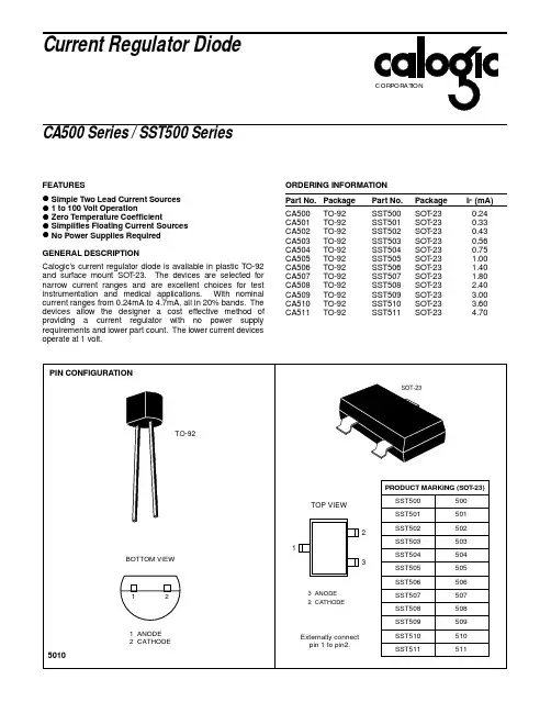
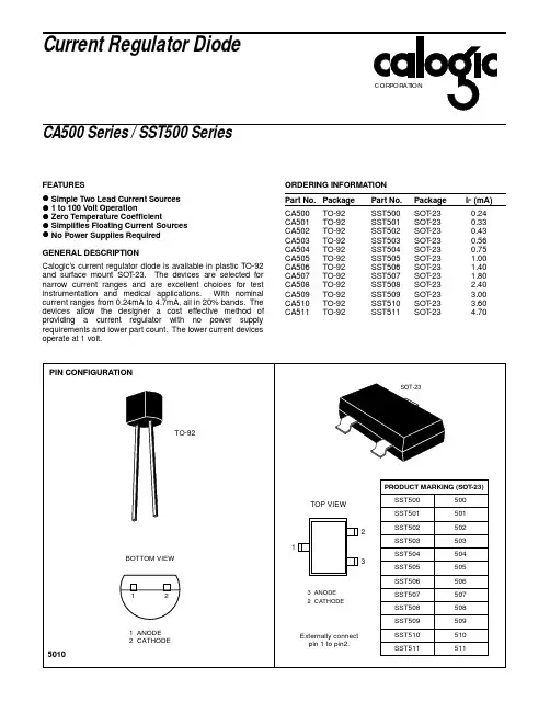
Features
• Black Surface and ColorTinted Epoxy• Industry Standard Size• Industry Standard Pinout• Choice of Character Size7.6 mm (0.30 in.), 10 mm(0.40in.), 14.2 mm (0.56 in.)• Choice of ColorsAlGaAs Red, High EfficiencyRed (HER), Green, Orange• Excellent AppearanceEvenly Lighted Segments±50° Viewing Angle• Design FlexibilityCommon Anode or CommonCathodeSingle and Two Digit• Categorized for LuminousIntensityCategorized for Color: GreenUse of Like Categories Yields aUniform Display• Excellent for Long DigitString Multiplexing
Description
These devices use industrystandard size package and pinout.Available with black surfaceHDSP-AX11/-AX13 SeriesHDSP-FX11/-FX13 SeriesHDSP-GX11/-GX13 SeriesHDSP-HX11/-HX13 SeriesHDSP-KX11/-KX13 Series
finish. All devices are available aseither common anode or commoncathode.
Typical applications includeappliances, channel indicators ofTV, CATV converters, gamemachines, and point of saleterminals.元器件交易网www.cecb2b.com2
Part Numbering System
Notes:1. For codes not listed in the figure above, please refer to the respective datasheet or contact your nearestAgilent representative for details.2. Bin options refer to shippable bins for a part number. Color and Intensity Bins are typically restricted to 1bin per tube (exceptions may apply). Please refer to respective datasheet for specific bin limit information.5082 -X X X X-X X X X XHDSP-X X X X-X X X X X
Mechanical Options[1]00: No Mechanical Option
Color Bin Options[1,2]0: No Color Bin Limitation
Maximum Intensity Bin[1,2]0: No Maximum Intensity Bin Limitation
Minimum Intensity Bin[1,2]0: No Minimum Intensity Bin Limitation
Device Configuration/Color[1]1: Common Anode3: Common Cathode
Device Specific Configuration[1]Refer to Respective Datasheet
Package[1]A: 7.6 mm (0.3 inch) Single Digit Seven Segment DisplayF: 10 mm (0.4 inch) Single Digit Seven Segment DisplayG: 10 mm (0.4 inch) Dual Digit Seven Segment DisplayH: 14.2 mm (0.56 inch) Single Digit Seven Segment DisplayK: 14.2 mm (0.56 inch) Dual Digit Seven Segment Display元器件交易网www.cecb2b.com3
Package Dimensions (7.6 mm Series)Internal Circuit Diagram
Package Dimensions (10 mm Series: Single)Internal Circuit Diagram元器件交易网www.cecb2b.com4
Package Dimensions (10 mm Series: Two Digit)Internal Circuit Diagram元器件交易网www.cecb2b.com5
Package Dimensions (14.2 mm Series: Single)Internal Circuit Diagram
Package Dimensions (14.2 mm Series: Two Digit)Internal Circuit Diagram
2
1DIGIT NO. 1 CATHODE元器件交易网www.cecb2b.com6AlGaAs Red
Device SeriesHDSP-ParameterSymbolMin.Typ.Max.Units Test Conditions
A11XLuminous Intensity/Segment[1,2]IV315600µcdIF = 1 mA(Digit Average)3600IF = 5 mA
F11X, G11X330650IF = 1 mA
3900IF = 5 mA
H11X, K11X400700IF = 1 mA
4200IF = 5 mA
All DevicesForward Voltage/Segment or DPVF1.62.0VIF = 1 mA
1.7IF = 5 mA
1.822IF = 20 mA Peak
Peak WavelengthλPEAK645nm
Dominant Wavelength[3]λd637nm
Reverse Voltage/Segment or DP[4]VR3.015V
IR = 100 µA
Temperature Coefficient of∆VF/°C-2mV/°CVF/Segment or DP
A11XThermal Resistance LEDRθJ-PIN255°C/W/Junction-to-PinSeg.F11X, G11X320
H11X, K12X400Electrical/Optical Characteristics at TA = 25°CAbsolute Maximum Ratings
AlGaAs RedHER/OrangeGreenHDSP-X11XHDSP-X21X/X41XHDSP-X51X DescriptionSeriesSeriesSeriesUnits
Average Power per Segment37105105mWor DP
Peak Forward Current per4590[1]90[3]mASegment or DP
DC Forward Current per15[5]30[2]30[4]mASegment or DP
Operating Temperature Range–20 to +100 –40 to +100°C
Storage Temperature Range–55 to +100°C
Reverse Voltage per3.0VSegment or DP
Wave Soldering Temperature for250°C3 Seconds (1.60 mm [0.063 in.]below Body)
Notes:1. See Figure 5 to establish pulsed conditions.2. Derate above 53°C at 0.45 mA/°C (see Figure 7).3. See Figure 6 to establish pulsed conditions.4. Derate above 39°C at 0.37 mA/°C (see Figure 7).5. Derate above 91°C at 0.53 mA/°C (see Figure 1).元器件交易网www.cecb2b.com