
LM8资料
- 格式:pdf
- 大小:2.72 MB
- 文档页数:2
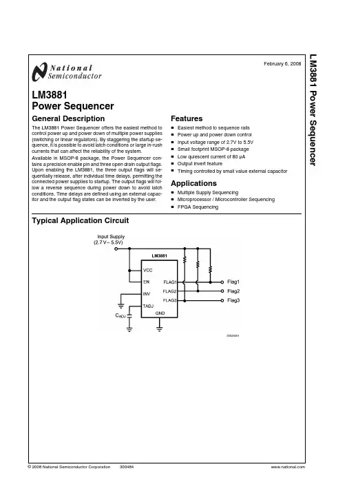
February 6, 2008 LM3881Power SequencerGeneral DescriptionThe LM3881 Power Sequencer offers the easiest method to control power up and power down of multiple power supplies (switching or linear regulators). By staggering the startup se-quence, it is possible to avoid latch conditions or large in-rush currents that can affect the reliability of the system. Available in MSOP-8 package, the Power Sequencer con-tains a precision enable pin and three open drain output flags. Upon enabling the LM3881, the three output flags will se-quentially release, after individual time delays, permitting the connected power supplies to startup. The output flags will fol-low a reverse sequence during power down to avoid latch conditions. Time delays are defined using an external capac-itor and the output flag states can be inverted by the user.Features■Easiest method to sequence rails■Power up and power down control■Input voltage range of 2.7V to 5.5V■Small footprint MSOP-8 package■Low quiescent current of 80 µA■Output invert feature■Timing controlled by small value external capacitor Applications■Multiple Supply Sequencing■Microprocessor / Microcontroller Sequencing■FPGA SequencingTypical Application Circuit30048401© 2008 National Semiconductor LM3881 Power SequencerConnection Diagram30048402Top View MSOP-8 PackageOrdering InformationOrder Number Package Type NSC Package DrawingSupplied AsLM3881MM MSOP-8MUA08A1000 Units on Tape and Reel LM3881MMX3500 Units on Tape and ReelPin DescriptionsPin #Name Function 1VCC Input Supply 2EN Precision Enable3GND Ground 4INV Output Logic Invert 5TADJ Timer Adjust 6FLAG3Open Drain Output #37FLAG2Open Drain Output #28FLAG1Open Drain Output #1 2L M 3881Absolute Maximum Ratings (Note 1)If Military/Aerospace specified devices are required, please contact the National Semiconductor Sales Office/ Distributors for availability and specifications.VCC, EN, INV, TADJ, FLAG1,FLAG2, FLAG3 to GND-0.3V to +6.0V Storage Temperature Range-65°C to +150°C Junction Temperature150°C Lead Temperature (Soldering, 5sec.)260°C Minimum ESD Rating (Note 2) 2 kV Operating Ratings(Note 1)VCC to GND 2.7V to 5.5V EN, INV, TADJ, FLAG1, FLAG2,FLAG3 to GND-0.3V to VCC + 0.3V Junction Temperature-40°C to +125°CElectrical Characteristics Specifications with standard typeface are for TJ= 25°C, and those in bold face typeapply over the full Operating Temperature Range (TJ= -40°C to +125°C). Minimum and Maximum limits are guaranteed throughtest, design or statistical correlation. Typical values represent the most likely parametric norm at TJ= 25°C and are provided forreference purposes only. VCC= 3.3V, unless otherwise specified.Symbol Parameter Conditions Min(Note 3)Typ(Note 4)Max(Note 3)UnitIQOperating Quiescent Current80110µA Open Drain FlagsI FLAG FLAGx Leakage Current VFLAGx= 3.3V0.0011µAV OL FLAGx Output Voltage Low IFLAGx= 1.2 mA0.4VTime DelaysITADJ_SRCTADJ Source Current41220µAITADJ_SNKTADJ Sink Current41220µAVHTHHigh Threshold Level 1.0 1.22 1.4VVLTHLow Threshold Level0.30.50.7VT CLK Clock Cycle CADJ= 10 nF 1.2msT D1, TD4Flag Time Delay910ClockCyclesT D2, TD3, TD5, TD6Flag Time Delay8ClockCyclesENABLE PinVENEN Pin Threshold 1.0 1.22 1.5VI EN EN Pin Pull-up Current VEN= 0V7µAINV PinVIH_INV Invert Pin VIH90%VCCVVIL_INV Invert Pin VIL10%VCCVNote 1:Absolute Maximum Ratings indicate limits beyond which damage to the device may occur. Operating Ratings indicate conditions for which the device isintended to be functional, but does not guarantee specific performance limits. For guaranteed specifications and conditions, see the Electrical Characteristics.Note 2:The human body model is a 100 pF capacitor discharged through a 1.5 kΩ resistor into each pin.Note 3:Limits are 100% production tested at 25°C. Limits over the operating temperature range are guaranteed through correlation using Statistical QualityControl (SQC) methods. The limits are used to calculate National's Average Outgoing Quality Level (AOQL).Note 4:Typical numbers are at 25°C and represent the most likely parametric norm.LM3881Typical Performance CharacteristicsV CC = 3.3V unless otherwise specified.Quiescent Current vs V CC30048414Quiescent Current vs Temperature30048415Enable Threshold vs Temperature30048416Time Delay vs V IN (C ADJ = 10 nF Nominal)30048417Time Delay vs Temperature (C ADJ = 10 nF Nominal)30048418V FLAG vs V IN(INV Low, R FLAG = 100 k Ω)30048419 4L M 3881FLAG Voltage vs Current30048420 LM3881Block Diagram30048403 6L M 3881Application InformationOVERVIEWThe LM3881 Power Sequencer provides a simple solution for sequencing multiple rails in a controlled manner. A clock sig-nal is established that facilitates control of the power up and power down of three open drain FET output flags. These flags permit connection to shutdown or enable pins of linear regu-lators and/or switching regulators to control the power sup-plies’ operation. This allows a complete power system to be designed without worrying about large in-rush currents or latch-up conditions that can occur during an uncontrolled startup. An invert (INV) pin is provided that reverses the logic of the output flags. This pin should be tied to a logic outputhigh or low and not allowed to remain open circuit. The fol-lowing discussion assumes the INV pin is held low such that the flag output is active high.A small external timing capacitor is connected to the TADJ pin that establishes the clock waveform. This capacitor is lin-early charged/discharged by a fixed current source/sink, de-noted ITADJ_SRC/ ITADJ_SNK, of magnitude 12 µA between pre-defined voltage threshold levels, denoted VLTHand VHTH, to generate the timing waveform as shown in the following dia-gram.30048409FIGURE 1. TADJ Pin Timing Waveform Thus, the clock cycle duration is directly proportional to thetiming capacitor value. Considering the TADJ voltage thresh-old levels and the charge/discharge current magnitude, it canbe shown that the timing capacitor-clock period relationshipis typically 120 µs/nF. For example, a 10 nF capacitor sets upa clock period of 1.2 ms.The timing sequence of the LM3881 is controlled by the en-able (EN) pin. Upon power up, all the flags are held low untilthe precision enable pin exceeds its threshold. After the ENpin is asserted, the power up sequence will commence andthe open-drain flags will be sequentially released.An internal counter will delay the first flag (FLAG1) from risinguntil a fixed time period, denoted by TD1 in the following timingdiagram, elapses. This corresponds to at least nine, maxi-mum ten, clock cycles depending on where EN is asserted relative to the clock signal. Upon release of the first flag, an-other timer will begin to delay the release of the second flag(FLAG2). This time delay, denoted TD2, corresponds to ex-actly eight clock periods. Similarly, FLAG3 is released aftertime delay TD3, again eight clock cycles, has expired. Accord-ingly, a TADJ capacitor of 10 nF generates typical time delaysTD2and TD3of 9.6 ms and TD1of between 10.8 ms and 12.0 ms.The power down sequence is the same as power up, but inreverse order. When the EN pin is de-asserted, a timer willbegin that delays the third flag (FLAG3) from pulling low. Thesecond and first flag will then follow in a sequential mannerafter their appropriate time delays. These time delays, denot-ed TD4, TD5, TD6, are equal to TD1, TD2, TD3, respectively.For robustness, the pull down FET associated with each flagis designed such that it can sustain a short circuit to VCC.LM388130048425FIGURE 2. Power Up Sequence, INV Low30048405FIGURE 3. Power Up Sequence, INV High 8L M 388130048406FIGURE 4. Power Down Sequence, INV Low30048424FIGURE 5. Power Down Sequence, INV High LM3881ENABLE CIRCUITThe enable circuit is designed with an internal comparator,referenced to a bandgap voltage (1.22V), to provide a preci-sion threshold. This allows the timing to be set externallyusing a capacitor as shown in the diagram below. Alterna-tively, sequencing can be based on a certain event such as aline voltage reaching 90% of its nominal value by employinga resistor divider from VCC to Enable.30048407FIGURE 6. Precision Enable CircuitUsing the internal pull-up current source to charge the exter-nal capacitor CEN, the time delay while the enable voltagereaches the required threshold, assuming EN is chargingfrom 0V, can be calculated by the equation as follows.30048404FIGURE 7. Enable Delay TimingA resistor divider can also be used to enable the LM3881based on exceeding a certain VCC supply voltage threshold.Care needs to be taken when sizing the resistor divider toinclude the effects of the internal EN pull-up current source.The supply voltage for which EN is asserted is given by30048410FIGURE 8. Enable Based On Input Supply LevelOne of the features of the enable pin is that it provides glitchfree operation. The timer will start counting at a rising thresh-old, but will always reset if the enable pin is de-assertedbefore the first output flag is released. This is illustrated in thetiming diagram below, assuming INV is low.30048411FIGURE 9. Enable Glitch Timing, INV LowIf the EN pin remains high for the entire power up sequence,then the part will operate as shown in the standard timing di-agrams. However, if the EN signal is de-asserted before thepower-up sequence is completed, the part will enter a con-trolled shutdown. This allows the system to initiate a con-trolled power sequence, preventing any latch conditions tooccur. The following timing diagrams describe the flag se-quence if the EN pin is de-asserted after FLAG1 releases, butbefore the entire power-up sequence is completed. INV is as-sumed low.10LM38813004841230048413FIGURE 10. Incomplete Sequence Timing, INV Low LM3881Physical Dimensions inches (millimeters) unless otherwise notedMSOP-8 PackageNS Package Number MUA08A 12L M 3881LM3881 NotesNotesL M 3881 P o w e r S e q u e n c e rFor more National Semiconductor product information and proven design tools, visit the following Web sites at:ProductsDesign SupportAmplifiers /amplifiers WEBENCH /webench Audio/audio Analog University /AU Clock Conditioners /timing App Notes /appnotes Data Converters /adc Distributors /contacts Displays /displays Green Compliance /quality/green Ethernet /ethernet Packaging/packaging Interface /interface Quality and Reliability /quality LVDS/lvds Reference Designs /refdesigns Power Management /power Feedback /feedback Switching Regulators /switchers LDOs /ldo LED Lighting /led PowerWise/powerwise Serial Digital Interface (SDI)/sdiTemperature Sensors /tempsensors Wireless (PLL/VCO)/wirelessTHE CONTENTS OF THIS DOCUMENT ARE PROVIDED IN CONNECTION WITH NATIONAL SEMICONDUCTOR CORPORATION (“NATIONAL”) PRODUCTS. NATIONAL MAKES NO REPRESENTATIONS OR WARRANTIES WITH RESPECT TO THE ACCURACY OR COMPLETENESS OF THE CONTENTS OF THI S PUBLI CATI ON AND RESERVES THE RI GHT TO MAKE CHANGES TO SPECI FI CATI ONS AND PRODUCT DESCRI PTI ONS AT ANY TI ME WI THOUT NOTI CE. NO LI CENSE, WHETHER EXPRESS,MPLI ED, ARI SI NG BY ESTOPPEL OR OTHERWI SE, TO ANY I NTELLECTUAL PROPERTY RI GHTS I S GRANTED BY THI S DOCUMENT.TESTI NG AND OTHER QUALI TY CONTROLS ARE USED TO THE EXTENT NATI ONAL DEEMS NECESSARY TO SUPPORT NATI ONAL’S PRODUCT WARRANTY. EXCEPT WHERE MANDATED BY GOVERNMENT REQUI REMENTS, TESTI NG OF ALL PARAMETERS OF EACH PRODUCT IS NOT NECESSAR ILY PERFORMED. NAT IONAL ASSUMES NO L IAB I L ITY FOR APPLI CATI ONS ASSI STANCE OR BUYER PRODUCT DESI GN. BUYERS ARE RESPONSI BLE FOR THEI R PRODUCTS AND APPLI CATI ONS USI NG NATI ONAL COMPONENTS. PRI OR TO USI NG OR DI STRI BUTI NG ANY PRODUCTS THAT I NCLUDE NATIONAL COMPONENTS, BUYERS SHOULD PROVIDE ADEQUATE DESIGN, TESTING AND OPERATING SAFEGUARDS.EXCEPT AS PROVIDED IN NATIONAL’S TERMS AND CONDITIONS OF SALE FOR SUCH PRODUCTS, NATIONAL ASSUMES NO LI ABI LI TY WHATSOEVER, AND NATI ONAL DI SCLAI MS ANY EXPRESS OR I MPLI ED WARRANTY RELATI NG TO THE SALE AND/OR USE OF NATIONAL PRODUCTS INCLUDING LIABILITY OR WARRANTIES RELATING TO FITNESS FOR A PARTICULAR PURPOSE, MERCHANTABI LI TY, OR I NFRI NGEMENT OF ANY PATENT, COPYRI GHT OR OTHER I NTELLECTUAL PROPERTY RIGHT.LIFE SUPPORT POLICYNATIONAL ’S PRODUCTS ARE NOT AUTHORIZED FOR USE AS CRITICAL COMPONENTS IN L IFE SUPPORT DEVICES OR SYSTEMS WITHOUT THE EXPRESS PRIOR WRITTEN APPROVAL OF THE CHIEF EXECUTIVE OFFICER AND GENERAL COUNSEL OF NATIONAL SEMICONDUCTOR CORPORATION. As used herein:Life support devices or systems are devices which (a) are intended for surgical implant into the body, or (b) support or sustain life and whose failure to perform when properly used in accordance with instructions for use provided in the labeling can be reasonably expected to result in a significant injury to the user. A critical component is any component in a life support device or system whose failure to perform can be reasonably expected to cause the failure of the life support device or system or to affect its safety or effectiveness.National Semiconductor and the National Semiconductor logo are registered trademarks of National Semiconductor Corporation. All other brand or product names may be trademarks or registered trademarks of their respective holders.Copyright© 2008 National Semiconductor CorporationFor the most current product information visit us at National Semiconductor Americas Technical Support Center Email:new.feedback@ Tel: 1-800-272-9959National Semiconductor Europe Technical Support CenterEmail: europe.support@ German Tel: +49 (0) 180 5010 771English Tel: +44 (0) 870 850 4288National Semiconductor Asia Pacific Technical Support Center Email: ap.support@National Semiconductor Japan Technical Support Center Email: jpn.feedback@。

LM358工作原理分析LM358是一种常用的双运算放大器,广泛应用于模拟电路中。
它由两个独立的运算放大器组成,具有高增益、宽带宽、低输入偏置电流和低输入偏置电压等特点。
本文将详细分析LM358的工作原理。
一、LM358的引脚功能及连接方式LM358一共有8个引脚,分别为:正电源(VCC+)、负电源(VCC-)、输入端1(IN1-)、输入端2(IN1+)、输出端1(OUT1)、输入端3(IN2-)、输入端4(IN2+)和输出端2(OUT2)。
在典型的应用中,LM358的引脚连接方式如下:1. 正电源(VCC+)和负电源(VCC-)引脚连接至电源电压,通常为+5V和-5V。
2. 输入端1(IN1-)和输入端2(IN1+)分别连接至输入信号源。
3. 输出端1(OUT1)连接至负载电阻。
4. 输入端3(IN2-)和输入端4(IN2+)连接至输入信号源。
5. 输出端2(OUT2)连接至负载电阻。
二、LM358的工作原理LM358是一种差分放大器,其工作原理可以分为输入级、差分放大级和输出级三个部分。
1. 输入级:输入级由差分放大器的输入端1(IN1-)和输入端2(IN1+)组成。
当输入信号加在IN1+引脚上,通过IN1-引脚反馈至负电源端,形成一个反相输入。
当输入信号加在IN1-引脚上,通过IN1+引脚反馈至正电源端,形成一个非反相输入。
通过输入级的差分放大作用,输入信号的微小变化可以被放大。
2. 差分放大级:差分放大级由输入级输出信号经过放大得到。
输入级的输出信号经过放大后,通过输出级的驱动,输出到OUT1引脚。
差分放大级的放大倍数可以通过调整输入级的电流和负载电阻来控制。
3. 输出级:输出级由输出端1(OUT1)和负载电阻组成。
输出级的作用是将差分放大级的输出信号经过电流放大和电压放大后,输出到负载电阻上。
LM358的输出电压可以通过调整输入级的电流和负载电阻来控制。
当输入信号的幅值较大时,输出电压会饱和,即达到正电源或负电源的电压。
