
MSK5232-2.5TD中文资料
- 格式:pdf
- 大小:254.40 KB
- 文档页数:6

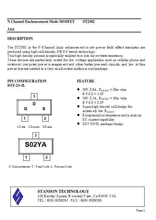
N Channel Enchancement Mode MOSFET ST2302 3.6A DESCRIPTION The ST2302 is the N-Channel logic enhancement mode power field effect transistor are produced using high cell density, DMOS trench technology. This high density process is especially tailored to minimize on-state resistance. These devices are particularly suited for low voltage application such as cellular phone and notebook computer power management and other batter powered circuits, and low in-line power loss are needed in a very small outine surface mount package. PIN CONFIGURATION SOT-23-3L
1.Gate 2.Source 3.Drain
S: Subcontractor Y: Year Code A: Process Code Page 1
STANSON TECHNOLOGY 120 Bentley Square, Mountain View, Ca 94040 USA TEL: (650) 9389294 FAX: (650) 9389295 FEATURE z 20V/3.6A, RDS(ON) = 80m-ohm @VGS = 4.5V z 20V/2.4A, RDS(ON) = 95m-ohm @VGS = 2.5V z Super high density cell design for extremely low RDS(ON) z Exceptional on-resistance and maximumDC current capability z SOT-23-3L package design 3

1. CONFIGURATION & DIMENSIONS :
3. ELECTRICAL CHARACTERISTICS ( @ 25°C ) :
SUPERWORLD ELECTRONICS (S) PTE LTD2. SCHEMATIC :DST5-24 (F) SERIESPOWER TRANSFORMER
PG. 1NOTE : Specifications subject to change without notice. Please check our website for latest information.15.01.2008gram317.5C35.81(1.410)BA7.62(.300)10.16(.400)101.6-1016.0 x 34.93Optional mtg.screw & nut*UNIT : mm (inch)36.80H(1.45)LVA48.50(1.91)W40.30(1.59)SIZE51231.75ML(1.250)PCB PatternABA35.31(1.390)78651.041(0.041)4321LHABA7.11(0.28)
6CWML
8 PINTYPE DST115/230V57843Clearance hole for optional mtg screw and nut
PC terminal
" " indicates polarity(4-40 x 1.375)
2150/60Hz
a. Primary VoltageAC 115/230 V 50/60 Hz .b. No Load Primary CurrentInput AC 115V 60Hz .Less Than 20mA .Input AC 230V 50Hz .Less Than 25mA .c. Secondary Voltage (±5%)Series AC 27.80V .Parallel AC 13.90V .d. Secondary Load CurrentSeries 0.5A .Parallel 1.0A .e. Full Load Primary CurrentInput AC 115V 60Hz .Less Than 75mA .Input AC 230V 50Hz .Less Than 145mA .f. Full Load Secondary Voltage (±5%)Series 24.00V .Pin 3-4Pin 1-2g. DC Resistance = 134.50 Ohm .Primary = 112.70 Ohm .Parallel 12.00V .Pin 5-6Pin 7-8h. Insulation Resistancei. Withstand Voltage (Hi-Pot)Secondary = 1.98 Ohm .= 2.27 Ohm .AC 2500V 60Hz 1 Minutes .Less Than 60 Deg C .EI-48 x 20.00 m/m .j. Temperature Risek. Core SizeDC 500V 100Meg Ohm Of More .元器件交易网
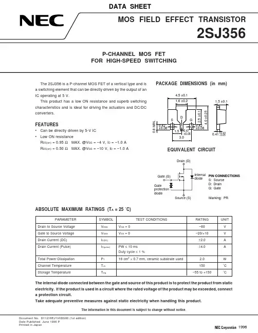
1996DATA SHEET
MOS FIELD EFFECT TRANSISTOR
2SJ356
P-CHANNEL MOS FETFOR HIGH-SPEED SWITCHING
Document No. D11218EJ1V0DS00 (1st edition)Date Published June 1996 PPrinted in JapanPACKAGE DIMENSIONS (in mm)
1.6 ±0.24.5 ±0.1
0.42 ±0.060.8 MIN.1.50.42 ±0.060.47 ±0.063.02.5 ±0.1
4.0 ±0.25
0.41+0.03–0.051.5 ±0.1
SDG
EQUIVALENT CIRCUIT
Source (S)Internal diodeGate protection diodeGate (G)Drain (D)
PIN CONNECTIONSS:D:G:SourceDrainGate
Marking: PRThe 2SJ356 is a P-channel MOS FET of a vertical type and isa switching element that can be directly driven by the output of anIC operating at 5 V.This product has a low ON resistance and superb switchingcharacteristics and is ideal for driving the actuators and DC/DCconverters.
FEATURES•Can be directly driven by 5-V IC•Low ON resistanceRDS(on) = 0.95 Ω MAX. @VGS = –4 V, ID = –1.0 ARDS(on) = 0.50 Ω MAX. @VGS = –10 V, ID = –1.0 A

AD8232
Rev. 0 Information furnished by Analog Devices is believed to be accurate and reliable. However, no responsibility is assumed by Analog Devices for its use, nor for any infringements of patents or other rights of third parties that may result from its use. Specications subject to change without notice. No license is granted by implication or otherwise under any patent or patent rights of Analog Devices. Trademarks and registered trademarks are the property of their respective owners. One Technology Way, P.O. Box 9106, Norwood, MA 02062-9106, U.S.A. Tel: 781.329.4700 Fax: 781.461.3113 ©2012 Analog Devices, Inc. All rights reserved. 功能框图
图1.
LOD–LOD+AD8232+VSGND
OUTOPAMP–REFOUTOPAMP+SWREFINIAOUTHPSENSEHPDRIVE+IN–IN
RLDRLDFBFR
SDNAC/DC
LEADS-OFFDETECTION10kΩ
10kΩ150kΩS1
S220
21341918171615IAA3