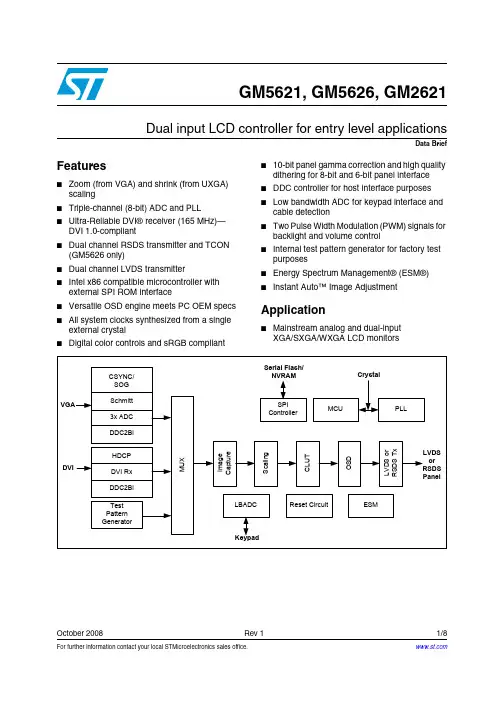
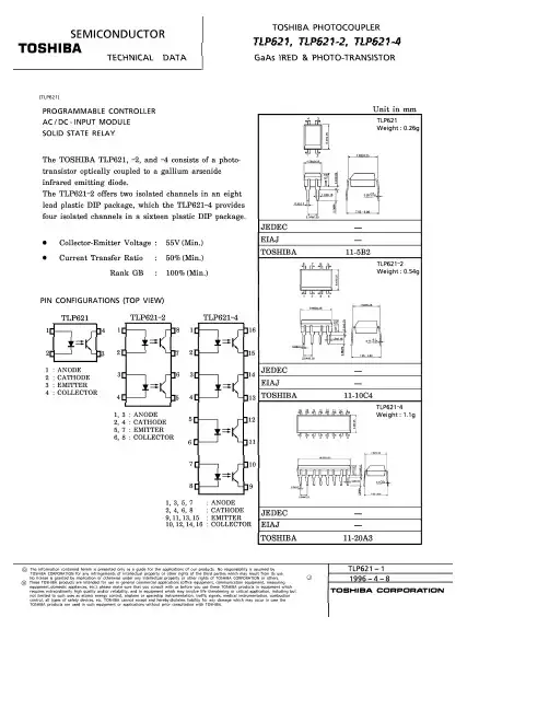
TLP621中文资料
- 格式:pdf
- 大小:423.97 KB
- 文档页数:8
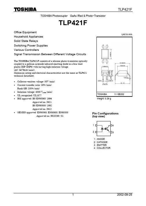
TOSHIBA Photocoupler GaAs IRed & Photo −TransistorTLP421FOffice EquipmentHousehold Appliances Solid State RelaysSwitching Power Supplies Various ControllersSignal Transmission Between Different Voltage CircuitsThe TOSHIBA TLP421F consists of a silicone photo −transistor optically coupled to a gallium arsenide infrared emitting diode in a four lead plastic DIP (DIP4) with having high isolation voltage (AC: 5kV RMS (min)).Maximum rating and electrical characteristics are the same as TLP421 technical datasheet.· Collector −emitter voltage: 80V (min) · Current transfer ratio: 50% (min)Rank GB: 100% (min)· Isolation voltage: 5000 V rms (min) · UL recognized: UL1577· BSI approved: BS EN60065: 1994Approved no. 8411 BS EN60950: 1992 Approved no. 8412 · SEMKO approved: EN60065, EN60950, EN60335Approved no. 9910249 / 01Pin Configurations(top view)121 : ANODE2 : CATHODE3 : EMITTER4 : COLLECTORUnit in mmTOSHIBA 11−5B202 Weight: 0.26 g· Option (D4) typeTUV approved: DIN VDE0884Approved no. R9950202Maximum operating insulation voltage: 1130V PKMaximum permissible over voltage: 8000V PK(Note): When a VDE0884 approved type is needed, please designate the “ Option (D4) ”Making VDE application: DIN VDE0884· Construction mehanical rating10.16mm pichTLP421F typeCreepage distance Clearance Insulation thickness 8.0 mm (min) 8.0 mm (min) 0.4 mm (min)· TOSHIBA is continually working to improve the quality and reliability of its products. Nevertheless, semiconductor devices in general can malfunction or fail due to their inherent electrical sensitivity and vulnerability to physical stress. It is the responsibility of the buyer, when utilizing TOSHIBA products, to comply with the standards of safety in making a safe design for the entire system, and to avoid situations in which a malfunction or failure of such TOSHIBA products could cause loss of human life, bodily injury or damage to property.In developing your designs, please ensure that TOSHIBA products are used within specified operating ranges as set forth in the most recent TOSHIBA products specifications. Also, please keep in mind the precautions and conditions set forth in the “Handling Guide for Semiconductor Devices,” or “TOSHIBA Semiconductor Reliability Handbook” etc.. · The TOSHIBA products listed in this document are intended for usage in general electronics applications (computer, personal equipment, office equipment, measuring equipment, industrial robotics, domestic appliances, etc.). These TOSHIBA products are neither intended nor warranted for usage in equipment that requires extraordinarily high quality and/or reliability or a malfunction or failure of which may cause loss of human life or bodily injury (“Unintended Usage”). Unintended Usage include atomic energy control instruments, airplane or spaceship instruments, transportation instruments, traffic signal instruments, combustion control instruments, medical instruments, all types of safety devices, etc.. Unintended Usage of TOSHIBA products listed in this document shall be made at the customer’s own risk. · Gallium arsenide (GaAs) is a substance used in the products described in this document. GaAs dust and fumes are toxic. Do not break, cut or pulverize the product, or use chemicals to dissolve them. When disposing of the products, follow the appropriate regulations. Do not dispose of the products with other industrial waste or with domestic garbage. · The products described in this document are subject to the foreign exchange and foreign trade laws.· The information contained herein is presented only as a guide for the applications of our products. No responsibility is assumed by TOSHIBA CORPORATION for any infringements of intellectual property or other rights of the third parties which may result from its use. No license is granted by implication or otherwise under any intellectual property or other rights of TOSHIBA CORPORATION or others. · The information contained herein is subject to change without notice.000707EBCRESTRICTIONS ON PRODUCT USE。