
AX3007-V1.2
- 格式:pdf
- 大小:613.65 KB
- 文档页数:12

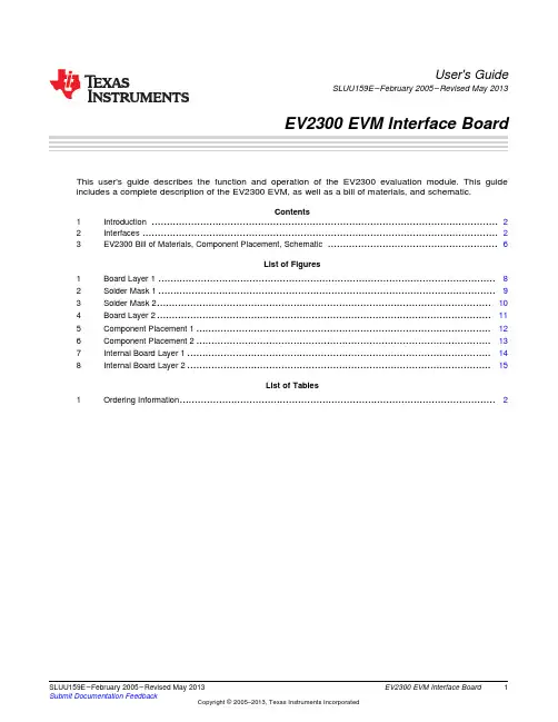
User's GuideSLUU159E–February2005–Revised May2013EV2300EVM Interface Board This user's guide describes the function and operation of the EV2300evaluation module.This guide includes a complete description of the EV2300EVM,as well as a bill of materials,and schematic.Contents1Introduction (2)2Interfaces (2)3EV2300Bill of Materials,Component Placement,Schematic (6)List of Figures1Board Layer1 (8)2Solder Mask1 (9)3Solder Mask2 (10)4Board Layer2 (11)5Component Placement1 (12)6Component Placement2 (13)7Internal Board Layer1 (14)8Internal Board Layer2 (15)List of Tables1Ordering Information (2)1 SLUU159E–February2005–Revised May2013EV2300EVM Interface Board Submit Documentation FeedbackCopyright©2005–2013,Texas Instruments IncorporatedIntroduction 1IntroductionThis EVM interface board enables an IBM-compatible or other type(with required driver for the particular platform)PC to communicate with Texas Instruments SMBus,HDQ,or DQ interface gas gauges via aUniversal Serial Bus(USB)port.In addition to this board,PC software is required to interpret the gasgauge data to complete the evaluation system.1.1Features•Fully powered from the USB port•Capable of providing a25-mA3.3-V source•Complete interface between USB and SMBus,I2C,and HDQ(8/16)interfaces using a simple API1.2Kit Contents•EV2300circuit module•Standard USB cable1.3Ordering InformationTable1.Ordering InformationEVM Part NumberEV23001.4FCC/IC Regulatory Compliance•FCC–FEDERAL COMMUNICATIONS COMMISSION Part15,Class A Compliant•IC–INDUSTRY CANADA Compliant2InterfacesThe EV2300interfaces are described in the following table.The reference designators on the circuit board and the functions are also listed.Reference Function FunctionDesignatorHDQ and SMB SMBus,HDQ,and DQ Interface ports Terminal block for connecting to a target deviceI2C E2PROM I2C Interface Terminal for connecting to a target E2PROM or I2C interfacebattery monitorUSB USB Interface Interface to host computer2EV2300EVM Interface Board SLUU159E–February2005–Revised May2013Submit Documentation FeedbackCopyright©2005–2013,Texas Instruments Incorporated Interfaces2.1OverviewThe EV2300is enclosed and is provided as shown.2.2EV2300ControllerThe EV2300controller is a bq8012running at 4MHz.The controller firmware is stored in flash memory and is executed by the core at power-up after the boot ROM code verifies the integrity words.The controller communicates with target device(s)through either:a 2-wire SMBus communication port,a 1-wire HDQ port,or a 2-wire E 2PROM I 2C port.The 2-wire SMBus communication port supports both SMBus and I 2C protocols.2.3USB Interface (USB)The interface board connects to a USB port (version 1.1)on a host computer and is powered from the port.All communication over the USB is proprietary and does not fit any USB-defined device classes.Therefore,communication with the device requires a loader and driver from Texas Instruments.The loader enumerates the device (determines it is present on the USB),then loads the EV2300controller firmware for the USB interface.Once the firmware load is complete,the loader sends a command to the USB interface IC to execute the new program and the loader driver exits.A new driver takes control and enumerates the EV2300and makes the device present to programs running on the host.The installer for the USB EVB installs:1.A loader driver2.A binary to load onto the USB interface IC3.An EV2300controller driver for direct access to the device4.An EV2300DLL for application access to the device3SLUU159E–February 2005–Revised May 2013EV2300EVM Interface Board Submit Documentation FeedbackCopyright ©2005–2013,Texas Instruments IncorporatedInterfaces 2.4HDQ Interface(HDQ)This interface allows a host computer to interact with a slave or target device through the two-wire SMBus or the one-wire HDQ interfaces.The ports are labeled with the corresponding signal names above each port connector.Connect the signal and a ground reference(GND),and optionally VOUT,to a targetdevice.The two-wire interface supports SMBus version1.1byte,word,block transactions with and without PEC.The SMBus limits the capacitance on each line(Data and Clock)to100pF.The EV2300places8pF on each line,so a device may place up to92pF total.If the capacitive load approaches or exceeds100pF, SMBus communication may not be reliable.Pin Name Description1GND Ground return/reference for HDQ interface2VOUT Controlled EEPROM power.Supplies5VDC to a target EEPROM IC3HDQ HDQ one-wire interface.Pulled up to3.3-V rail with a10-kΩresistor4VCC Supplies3.3VDC to a target.Current load should be limited to30mA2.5I2C/EEPROM Interface(I2C)This interface allows a host computer to interact with a target E2PROM or other I2C interface device such as a battery monitor device through a two-wire I2C interface.The interface contains a controlled power pin, the I2C clock and data lines,and a ground reference.Pin Name Description1GND Ground return.Connected to the SMD and HDQ GND2SCL I2C clock.This line must be pulled up by the target.3SDA I2C data.This line must be pulled up by the target.4VOUT Controlled EEPROM power.Supplies5VDC to a target EEPROM IC4EV2300EVM Interface Board SLUU159E–February2005–Revised May2013Submit Documentation FeedbackCopyright©2005–2013,Texas Instruments Incorporated Interfaces 2.6SMBus Interface(SMBus)Pin Name Description1GND Ground reference2SMBC SMB clock pin.This pin is pulled to3.3VDC through a10-kΩresistor.Do not exceed5.6VDC onthis pin.3SMBD SMB data pin.This pin is pulled to3.3VDC through a10-kΩresistor.Do not exceed5.6VDC onthis pin.4NC Not connected on this board.This pin is floating.5 SLUU159E–February2005–Revised May2013EV2300EVM Interface Board Submit Documentation FeedbackCopyright©2005–2013,Texas Instruments Incorporated3EV2300Bill of Materials,Component Placement,SchematicThis chapter includes the schematic,component placement on the circuit board,and a listing of the bill of materials for the EV2300EVM.3.1Bill of Materials(BOM)Qty Ref Des(1)Description(2)(3)(4)Size MFR Part Number10C1-C7,C10-Capacitor,ceramic,0.1µF,25V,X7R,10%603TDK C1608X7R1E104KT C12,C15,C200C13Open6032C16,C21Capacitor,POSCAP4.7µF,35V,20%6032©)AVX TAJC475K035R1C18Capacitor,ceramic,2200pF,50V,C0G,10%603TDK C1608C0G1H222KT1C19Capacitor,ceramic,150pF,50V,C0G,10%603TDK C1608C0G1H151KT2C8,C9Capacitor,ceramic,22pF,50V,C0G,10%603TDK C1608C0G1H220KT0D1-D7,D9,Open0.068×0.049D13-D15,D172D12,D19Diode,LED,green,20mA,0.9mcd0.068×0.049Panasonic LN1371G-(TR)1D20Diode,LED,red,20mA,0.9mcd0.068×0.049Panasonic LN1271R-(TR)3D21-D23Diode,dual,250mA,70V SOT23Vishay-Liteon BAW56GS085D8,D10,Diode,low capacitance,TVS SOT23General Semi GL05T D11,D16,D181J1Connector,USB upstream(Type B)0.47"×0.67"Molex67068-10003J13-J15Header,friction lock assembly,4-pin right angle0.400x0.500Molex22-05-30411J2Header,11pin,100mil spacing,(36-pin strip)121100Sullins PTC36SAAN0J3-J5,J8-Open0.038"J111J7Header,2pin,100mil spacing,(36-pin strip)0.100×2"Sullins PTC36SAAN1Q1Transistor,NPN,high-performance,500mA SOT23Fairchild MMBT2222A1Q2MOSFET,P-ch,–12V,4A,51mΩSOT23Vishay Si2335DS4R1,R14,Resistor,chip,10kΩ,1/16W,5%603Std StdR16,R1912R13,R15,Resistor,chip,100Ω,1/16W,5%603Std StdR21–R24,R26,R27,R45,R46,R49,R503R18,R42,Resistor,chip,1MΩ,1/16W,1%603Std StdR431R2Resistor,chip,15kΩ,1/16W,5%603Std Std7R3–R5,Resistor,chip,100kΩ,1/16W,5%603Std StdR32–R34,R393R30,R51,Resistor,chip,620Ω,1/16W,5%603Std StdR522R31,R41Resistor,chip,10Ω,1/16W,5%603Std Std1R35Resistor,chip,61.9kΩ,1/16W,1%603Std Std1R53Resistor,chip,0Ω,1/16W,5%603Std Std(1)Reference designators marked with an asterisk(*)cannot be substituted.All other components can be substituted withequivalent manufacturers components.(2)These assemblies are ESD sensitive,ESD precautions should be observed.(3)These assemblies must be clean and free from flux and all e of no clean flux is not acceptable.(4)These assemblies must comply with workmanship standards IPC-A-610Class2.6EV2300EVM Interface Board SLUU159E–February2005–Revised May2013Submit Documentation FeedbackCopyright©2005–2013,Texas Instruments IncorporatedQty Ref Des(1)Description(2)(3)(4)Size MFR Part Number1R54Resistor,chip,113kΩ,1/16W,0.1%603Vishay TNPW06031133BT9RT1 1R6Resistor,chip,1.5kΩ,1/16W,5%603Std Std0R7,R10-Open603R12,R17,R20,R25,R28,R36-R38,R402R8,R9Resistor,chip,33Ω,1/16W,5%603Std Std0SW1Open5mm×5mm2U1,U2IC,Single bus buffer gate with3-state output,with DCK TI SN74LVC1G125DCK negative enable1U3IC,Single bus buffer gate with3-state output,with DCK TI SN74LVC1G126DCK positive enable1U4IC,USB,general purpose,device controller0.480×TI TUSB3210PM0.480"1U5IC,ultra low-power LDO regulator,3.3V,50mA SOT23-5TI TPS77033DBV1U6IC,Advance gas gauge DBT38TI bq8015DBT1Y1or Y4Crystal,high performance,12.00MHz,SMT0.126×0.126Citizen or CSA-309-12.000MABJDaishinku or DSX630G-12.00MHz 0Y2or Y3Crystal,32.768MHz,7-12pF capacitance1,9mm×5Daishinku or DST520G-32.768kHzmm ECS or ECS-0.327-8-14 1N/A Plastic enclosure,bone,Texas Instruments PacTec84107-501-039silkscreenWire Cable Assembly(5)1Mate Connector,female,0.100centers22-01-3047Molex4N/A Terminals,crimp,tin08-50-0114Molex N/A Wire,insulated22Awg,red,18inches(±3inches)Any Any(VOUT)N/A Wire,insulated22Awg,white,18inches(±3inches)Any Any(SCL)N/A Wire,insulated22Awg,black,18inches(±3inches)Any Any(GND)N/A Wire,insulated22Awg,brown,18inches(±3Any Anyinches)(SDA)1N/A Heatshrink1"Any Any(5)Make one EEPROM connector wire assembly for each assembly produced,from J15mate,4-22AWG wires and crimpterminals.Wire colors for pin numbers are listed below.Strip and tin flying leads0.25inches from end of wire.Red-pin#4(signal VOUT)Brown-pin#3(signal SDA)White-pin#2(signal SCL)Black-pin#1(GND)7 SLUU159E–February2005–Revised May2013EV2300EVM Interface Board Submit Documentation FeedbackCopyright©2005–2013,Texas Instruments Incorporated3.2EV23008EV2300EVM Interface Board SLUU159E–February2005–Revised May2013Submit Documentation FeedbackCopyright©2005–2013,Texas Instruments IncorporatedFigure2.Solder Mask19 SLUU159E–February2005–Revised May2013EV2300EVM Interface Board Submit Documentation FeedbackCopyright©2005–2013,Texas Instruments IncorporatedFigure3.Solder Mask210EV2300EVM Interface Board SLUU159E–February2005–Revised May2013Submit Documentation FeedbackCopyright©2005–2013,Texas Instruments IncorporatedFigure4.Board Layer211 SLUU159E–February2005–Revised May2013EV2300EVM Interface Board Submit Documentation FeedbackCopyright©2005–2013,Texas Instruments Incorporatedponent Placement112EV2300EVM Interface Board SLUU159E–February2005–Revised May2013Submit Documentation FeedbackCopyright©2005–2013,Texas Instruments Incorporatedponent Placement213 SLUU159E–February2005–Revised May2013EV2300EVM Interface Board Submit Documentation FeedbackCopyright©2005–2013,Texas Instruments IncorporatedFigure7.Internal Board Layer114EV2300EVM Interface Board SLUU159E–February2005–Revised May2013Submit Documentation FeedbackCopyright©2005–2013,Texas Instruments Incorporated15 SLUU159E–February2005–Revised May2013EV2300EVM Interface Board Submit Documentation FeedbackCopyright©2005–2013,Texas Instruments Incorporated3.3EV2300Schematic16EV2300EVM Interface Board SLUU159E–February2005–Revised May2013Submit Documentation FeedbackCopyright©2005–2013,Texas Instruments IncorporatedEVALUATION BOARD/KIT/MODULE(EVM)ADDITIONAL TERMSTexas Instruments(TI)provides the enclosed Evaluation Board/Kit/Module(EVM)under the following conditions:The user assumes all responsibility and liability for proper and safe handling of the goods.Further,the user indemnifies TI from all claims arising from the handling or use of the goods.Should this evaluation board/kit not meet the specifications indicated in the User’s Guide,the board/kit may be returned within30days from the date of delivery for a full refund.THE FOREGOING LIMITED WARRANTY IS THE EXCLUSIVE WARRANTY MADE BY SELLER TO BUYER AND IS IN LIEU OF ALL OTHER WARRANTIES,EXPRESSED,IMPLIED,OR STATUTORY,INCLUDING ANY WARRANTY OF MERCHANTABILITY OR FITNESS FOR ANY PARTICULAR PURPOSE.EXCEPT TO THE EXTENT OF THE INDEMNITY SET FORTH ABOVE,NEITHER PARTY SHALL BE LIABLE TO THE OTHER FOR ANY INDIRECT,SPECIAL,INCIDENTAL,OR CONSEQUENTIAL DAMAGES.Please read the User's Guide and,specifically,the Warnings and Restrictions notice in the User's Guide prior to handling the product.This notice contains important safety information about temperatures and voltages.For additional information on TI's environmental and/or safety programs,please visit /esh or contact TI.No license is granted under any patent right or other intellectual property right of TI covering or relating to any machine,process,or combination in which such TI products or services might be or are used.TI currently deals with a variety of customers for products,and therefore our arrangement with the user is not exclusive.TI assumes no liability for applications assistance,customer product design, software performance,or infringement of patents or services described herein.REGULATORY COMPLIANCE INFORMATIONAs noted in the EVM User’s Guide and/or EVM itself,this EVM and/or accompanying hardware may or may not be subject to the Federal Communications Commission(FCC)and Industry Canada(IC)rules.For EVMs not subject to the above rules,this evaluation board/kit/module is intended for use for ENGINEERING DEVELOPMENT, DEMONSTRATION OR EVALUATION PURPOSES ONLY and is not considered by TI to be a finished end product fit for general consumer use.It generates,uses,and can radiate radio frequency energy and has not been tested for compliance with the limits of computing devices pursuant to part15of FCC or ICES-003rules,which are designed to provide reasonable protection against radio frequency interference.Operation of the equipment may cause interference with radio communications,in which case the user at his own expense will be required to take whatever measures may be required to correct this interference.General Statement for EVMs including a radioUser Power/Frequency Use Obligations:This radio is intended for development/professional use only in legally allocated frequency and power limits.Any use of radio frequencies and/or power availability of this EVM and its development application(s)must comply with local laws governing radio spectrum allocation and power limits for this evaluation module.It is the user’s sole responsibility to only operate this radio in legally acceptable frequency space and within legally mandated power limitations.Any exceptions to this are strictly prohibited and unauthorized by Texas Instruments unless user has obtained appropriate experimental/development licenses from local regulatory authorities,which is responsibility of user including its acceptable authorization.For EVMs annotated as FCC–FEDERAL COMMUNICATIONS COMMISSION Part15CompliantCautionThis device complies with part15of the FCC Rules.Operation is subject to the following two conditions:(1)This device may not cause harmful interference,and(2)this device must accept any interference received,including interference that may cause undesired operation. Changes or modifications not expressly approved by the party responsible for compliance could void the user's authority to operate the equipment.FCC Interference Statement for Class A EVM devicesThis equipment has been tested and found to comply with the limits for a Class A digital device,pursuant to part15of the FCC Rules. These limits are designed to provide reasonable protection against harmful interference when the equipment is operated in a commercial environment.This equipment generates,uses,and can radiate radio frequency energy and,if not installed and used in accordance with the instruction manual,may cause harmful interference to radio communications.Operation of this equipment in a residential area is likely to cause harmful interference in which case the user will be required to correct the interference at his own expense.FCC Interference Statement for Class B EVM devicesThis equipment has been tested and found to comply with the limits for a Class B digital device,pursuant to part15of the FCC Rules. These limits are designed to provide reasonable protection against harmful interference in a residential installation.This equipment generates,uses and can radiate radio frequency energy and,if not installed and used in accordance with the instructions,may cause harmful interference to radio communications.However,there is no guarantee that interference will not occur in a particular installation.If this equipment does cause harmful interference to radio or television reception,which can be determined by turning the equipment off and on,the user is encouraged to try to correct the interference by one or more of the following measures:•Reorient or relocate the receiving antenna.•Increase the separation between the equipment and receiver.•Connect the equipment into an outlet on a circuit different from that to which the receiver is connected.•Consult the dealer or an experienced radio/TV technician for help.For EVMs annotated as IC–INDUSTRY CANADA CompliantThis Class A or B digital apparatus complies with Canadian ICES-003.Changes or modifications not expressly approved by the party responsible for compliance could void the user’s authority to operate the equipment.Concerning EVMs including radio transmittersThis device complies with Industry Canada licence-exempt RSS standard(s).Operation is subject to the following two conditions:(1)this device may not cause interference,and(2)this device must accept any interference,including interference that may cause undesired operation of the device.Concerning EVMs including detachable antennasUnder Industry Canada regulations,this radio transmitter may only operate using an antenna of a type and maximum(or lesser)gain approved for the transmitter by Industry Canada.To reduce potential radio interference to other users,the antenna type and its gain should be so chosen that the equivalent isotropically radiated power(e.i.r.p.)is not more than that necessary for successful communication.This radio transmitter has been approved by Industry Canada to operate with the antenna types listed in the user guide with the maximum permissible gain and required antenna impedance for each antenna type indicated.Antenna types not included in this list,having a gain greater than the maximum gain indicated for that type,are strictly prohibited for use with this device.Cet appareil numérique de la classe A ou B est conformeàla norme NMB-003du Canada.Les changements ou les modifications pas expressément approuvés par la partie responsable de la conformitéont pu vider l’autoritédel'utilisateur pour actionner l'équipement.Concernant les EVMs avec appareils radioLe présent appareil est conforme aux CNR d'Industrie Canada applicables aux appareils radio exempts de licence.L'exploitation est autorisée aux deux conditions suivantes:(1)l'appareil ne doit pas produire de brouillage,et(2)l'utilisateur de l'appareil doit accepter tout brouillage radioélectrique subi,même si le brouillage est susceptible d'en compromettre le fonctionnement.Concernant les EVMs avec antennes détachablesConformémentàla réglementation d'Industrie Canada,le présentémetteur radio peut fonctionner avec une antenne d'un type et d'un gain maximal(ou inférieur)approuvépour l'émetteur par Industrie Canada.Dans le but de réduire les risques de brouillage radioélectriqueàl'intention des autres utilisateurs,il faut choisir le type d'antenne et son gain de sorte que la puissance isotrope rayonnéeéquivalente (p.i.r.e.)ne dépasse pas l'intensiténécessaireàl'établissement d'une communication satisfaisante.Le présentémetteur radio aétéapprouvépar Industrie Canada pour fonctionner avec les types d'antenneénumérés dans le manueld’usage et ayant un gain admissible maximal et l'impédance requise pour chaque type d'antenne.Les types d'antenne non inclus dans cette liste,ou dont le gain est supérieur au gain maximal indiqué,sont strictement interdits pour l'exploitation de l'émetteur.【Important Notice for Users of this Product in Japan】This development kit is NOT certified as Confirming to Technical Regulations of Radio Law of JapanIf you use this product in Japan,you are required by Radio Law of Japan to follow the instructions below with respect to this product:e this product in a shielded room or any other test facility as defined in the notification#173issued by Ministry of Internal Affairs andCommunications on March28,2006,based on Sub-section1.1of Article6of the Ministry’s Rule for Enforcement of Radio Law of Japan,e this product only after you obtained the license of Test Radio Station as provided in Radio Law of Japan with respect to thisproduct,ore of this product only after you obtained the Technical Regulations Conformity Certification as provided in Radio Law of Japan withrespect to this product.Also,please do not transfer this product,unless you give the same notice above to the transferee.Please note that if you could not follow the instructions above,you will be subject to penalties of Radio Law of Japan.Texas Instruments Japan Limited(address)24-1,Nishi-Shinjuku6chome,Shinjuku-ku,Tokyo,Japanhttp://www.tij.co.jp【ご使用にあたっての注】本開発キットは技術基準適合証明を受けておりません。

软件升级步骤!重要提示更新软件必须从雅马哈官方网站下载;谨遵说明操作,不要试图操作其他没有具体说明的雅马哈软件程序;如果不通过雅马哈官网下载的更新软件或者没有按照更新说明操作而造成的功放不能正常使用,雅马哈将不提供售后服务保障。
您可以从以下两种方法中选择一种方法,更新至最新版本的软件。
(需要连接至互联网)(需要USB闪存)通过互联网升级软件要求:连接互联网使您的功放连接至互联网并能接收网络电台。
(详情请参考说明书)1、关闭收音扩音机(待机状态)2、进入ADV ANCED SETUP模式按下MAIN ZONE按钮,同时按住STRAIGHT不放直到前面板显示“ADV ANCED SETUP”。
*“ADV ANCED SETUP”仅显示几秒钟。
3、从菜单中选择“FIRM UPDATE”a. 按住PROGRAM按钮直至“FIRM UPDATE USB”字样显示。
b. 接着,按住STRAIGHT按钮直至“NETWORK”字样显示。
4、开始软件升级a. 按下INFO按钮开始升级。
(升级过程可能需要15分钟)* 如果出现“UPDATE UNA V AIL”,表明您的收音扩音机准备好可以升级了。
此时,关闭电源从ADV ANCED SETUP中退出。
您的收音扩音机可以正常使用了。
软件升级过程中!警告升级过程中请不要中断电源。
万一升级过程中突然断电,致使无法恢复正常操作,请参考最后页的故障指南(案例2)。
b. 升级完成,“UPDATE SUCCESS”字样显示。
RX-V3067/2067/1067c. 按下MAIN ZONE按钮,关闭电源。
5、检查更新后的软件版本a.打开收音扩音机,按下遥控器上的ON SCREEN按钮。
b.选择“Information” > “System”。
c.确认软件版本已经升级至最新版。
恭喜!您已经完成了软件升级。
您的收音扩音机现在可以正常使用了。
通过USB 闪存升级软件要求:USB 闪存,可存储25MB 容量以上的内存。

General DescriptionThe MAX3050/MAX3057 interface between the CAN protocol controller and the physical wires of the bus lines in a controller area network (CAN). They are pri-marily intended for automotive systems requiring data rates up to 2Mbps and feature ±80V fault protection against short circuits in high-voltage power buses. They provide differential transmit capability to the bus and differential receive capability to the CAN controller. The MAX3050/MAX3057 have four modes of operation:high speed, slope control, standby, and shutdown.High-speed mode allows data rates up to 2Mbps. In slope-control mode, data rates are 40kbps to 500kbps,so the effects of EMI are reduced, and unshielded twisted or parallel cable can be used. In standby mode,the transmitters are shut off and the receivers are put into low-current mode. In shutdown mode, the transmit-ter and receiver are switched off.The MAX3050 has an AutoShutdown™ function that puts the device into a 15µA shutdown mode when the bus or CAN controller is inactive for 4ms or longer.The MAX3050/MAX3057 are available in an 8-pin SO package and are specified for operation from -40°C to +125°C.ApplicationsAutomotive Systems HVAC Controls Telecom 72V systemsFeatureso ±80V Fault Protection for 42V Systems o Four Operating ModesHigh-Speed Operation Up to 2Mbps Slope-Control Mode to Reduce EMI (40kbps to 500kbps)Standby ModeLow-Current Shutdown Mode o AutoShutdown when Device Is Inactive (MAX3050)o Automatic Wake-Up from Shutdown (MAX3050)o Thermal Shutdown o Current Limitingo Fully Compatible with the ISO 11898 Standard*MAX3050/MAX3057±80V Fault-Protected, 2Mbps, Low SupplyCurrent CAN Transceivers________________________________________________________________Maxim Integrated Products 1Ordering InformationTypical Operating Circuit19-2670; Rev 0; 10/02For pricing, delivery, and ordering information,please contact Maxim/Dallas Direct!at1-888-629-4642, or visit Maxim’s website at .Pin ConfigurationAutoShutdown is a trademark of Maxim Integrated Products, Inc.*Pending completion of testing.M A X 3050/M A X 3057±80V Fault-Protected, 2Mbps, Low Supply Current CAN Transceivers 2_______________________________________________________________________________________ABSOLUTE MAXIMUM RATINGSDC ELECTRICAL CHARACTERISTICS(V CC = +5V ±10%, R L = 60Ω, RS = GND, T A = T MIN to T MAX . Typical values are at V CC = +5V and T A = +25°C.)Stresses beyond those listed under “Absolute Maximum Ratings” may cause permanent damage to the device. These are stress ratings only, and functional operation of the device at these or any other conditions beyond those indicated in the operational sections of the specifications is not implied. Exposure to absolute maximum rating conditions for extended periods may affect device reliability.V CC to GND ............................................................-0.3V to +6V TXD, RS, RXD, SHDN to GND....................-0.3V to (V CC + 0.3V)CANH, CANL to GND..............................................-80V to +80V RXD Shorted to GND.................................................Continuous Continuous Power Dissipation (T A = +70°C)8-Pin SO (derate 5.9mW/°C above +70°C) .................470mWOperating Temperature Range .........................-40°C to +125°C Junction Temperature......................................................+150°C Storage Temperature Range.............................-65°C to +150°C Lead Temperature (soldering, 10s) ................................+300°CMAX3050/MAX3057±80V Fault-Protected, 2Mbps, Low SupplyCurrent CAN Transceivers_______________________________________________________________________________________3DC ELECTRICAL CHARACTERISTICS (continued)M A X 3050/M A X 3057±80V Fault-Protected, 2Mbps, Low Supply Current CAN Transceivers 4_______________________________________________________________________________________Note 1:As defined by ISO, bus value is one of two complementary logical values: dominant or recessive. The dominant value repre-sents the logical 1 and the recessive represents the logical 0. During the simultaneous transmission of the dominant and recessive bits, the resulting bus value is dominant. For MAX3050 and MAX3057 values, see the truth table in the Transmitter and Receiver sections.TIMING CHARACTERISTICSMAX3050/MAX3057±80V Fault-Protected, 2Mbps, Low SupplyCurrent CAN Transceivers_______________________________________________________________________________________5Figure 1. AC Test CircuitFigure 2. Timing Diagram for Dynamic Characteristics Figure 3. Time to Wake Up (t WAKE ) (MAX3050)M A X 3050/M A X 3057±80V Fault-Protected, 2Mbps, Low Supply Current CAN Transceivers 6_______________________________________________________________________________________Typical Operating Characteristics(V CC = 5V, R L = 60Ω, C L = 100pF, T A = +25°C, unless otherwise specified.)MAX3057SLEW RATE vs. R RSR RS (k Ω)S L E W R A T E (V /µs )1621248648510152025010200M A X 50 t o c 02S L E E P T I M E (m s )3002001002040608010000400MAX3050AutoShutdown vs. C SHDNC SHDN (nF)SUPPLY CURRENT vs. DATA RATEDATA RATE (kbps)S U P P L Y C U R R E N T (m A )160012008004002729313335252000RECEIVER PROPAGATION DELAY vs. TEMPERATURE, R RS = GNDTEMPERATURE (°C)R E C E I V E R P R O P A G A T I O N D E L A Y (n s )905520-15253545556515-50125DRIVER PROPAGATION DELAY vs. TEMPERATURE, R RS = GNDTEMPERATURE (°C)D R I VE R P R O P A G A T I O N D E L A Y (n s )925926-72025303515-40125RECEIVER OUTPUT LOW vs. OUTPUT CURRENTOUTPUT CURRENT (mA)V O L T A G E R X D (m V )2015105400800120016000025RECEIVER OUTPUT HIGH vs. OUTPUT CURRENTOUTPUT CURRENT (mA)V O L T A G E (V C C - R X D ) (m V )201510560012001800300024000025DIFFERENTIAL VOLTAGE vs. DIFFERENTIAL LOAD R LDIFFERENTIAL LOAD R L (Ω)D I F FE R E N T I A L V O L T A G E (V )25020015010050123400300SUPPLY CURRENTvs. TEMPERATURE IN STANDBY MODEM A X 3050 t o c 09TEMPERATURE (°C)S U P P L Y C U R R E N T (µA )905520-157510012515017520050-50125MAX3050/MAX3057±80V Fault-Protected, 2Mbps, Low SupplyCurrent CAN TransceiversLOOPBACK PROPAGATION DELAY vs. R RSM A X 350 t o c 10R RS (k Ω)L O O P B A C K P R O P A G A T I O N D E L A Y (n s )1501005020040060080010001200140000200RECEIVER PROPAGATION DELAYMAX3050 toc1140ns/divRXD 2V/divCANH - CANLDRIVER PROPAGATION DELAYMAX3050 toc131µs/divTXD 5V/divR RS = 24k ΩR RS = 100k ΩR RS = 180k ΩDRIVER PROPAGATION DELAY40ns/divTXD 2V/div CANH - CANLTypical Operating Characteristics (continued)(V CC = 5V, R L = 60Ω, C L = 100pF, T A = +25°C, unless otherwise specified.)Pin DescriptionM A X 3050/M A X 3057Detailed DescriptionThe MAX3050/MAX3057 interface between the protocol controller and the physical wires of the bus lines in a CAN. They are primarily intended for automotive appli-cations requiring data rates up to 2Mbps and feature ±80V fault protection against shorts in high-voltage sys-tems. This fault protection allows the devices to with-stand up to ±80V with respect to ground with no damage to the device. The built-in fault tolerance allows the device to survive in industrial and automotive environments with no external protection devices. The devices provide differential transmit capability to the bus and differential receive capability to the CAN con-troller (Figure 4).The device has four modes of operation: high speed,slope control, standby, and shutdown. In high-speed mode, slew rates are not limited, making 2Mbps transmis-sion speeds possible. Slew rates are controlled in slope-control mode, minimizing EMI and allowing use of unshielded twisted or parallel cable. In standby mode,receivers are active and transmitters are in high imped-ance. In shutdown mode, transmitters and receivers are turned off.The transceivers are designed to operate from a single +5V supply and draw 56mA of supply current in domi-nant state and 3.6mA in recessive state. In standby mode, supply current is reduced to 125µA. In shutdown mode, supply current is 15µA.CANH and CANL are output short-circuit current limited and are protected against excessive power dissipation by thermal-shutdown circuitry that places the driver outputs into a high-impedance state.Fault ProtectionThe MAX3050/MAX3057 feature ±80V fault protection.This extended voltage range of CANH and CANL bus lines allows use in high-voltage systems and communi-cation with high-voltage buses. If data is transmitting at 2Mbps, the fault protection is reduced to ±70V.TransmitterThe transmitter converts a single-ended input (TXD)from the CAN controller to differential outputs for the bus lines (CANH, CANL). The truth table for the trans-mitter and receiver is given in Table 1.±80V Fault-Protected, 2Mbps, Low Supply Current CAN Transceivers 8_______________________________________________________________________________________Figure 4. Functional DiagramHigh SpeedConnect RS to ground to set the MAX3050/MAX3057 to high-speed mode. When operating in high-speed mode, the MAX3050/MAX3057 can achieve transmis-sion rates of up to 2Mbps. Line drivers are switched on and off as quickly as possible. However, in this mode,no measures are taken to limit the rise and fall slope of the data signal, allowing for potential EMI emissions. If using the MAX3050/MAX3057 in high-speed mode, use shielded twisted-pair cable to avoid EMI problems.Slope ControlConnect a resistor from RS to ground to select slope-control mode (Table 2). In slope-control mode, the gates of the line drivers are charged with a controlled current, proportional to the resistor connected to the RS pin. Transmission speed ranges from 40kbps to 500kbps. Controlling the rise and fall slope reduces EMI and allows the use of an unshielded twisted pair or a parallel pair of wires as bus lines. The transfer func-tion for selecting the resistor value is given by:R RS (k Ω) = 12000/speed (in kbps)See the Slew Rate vs. R RS graph in the Typical Operating Characteristics section.ReceiverThe receiver reads differential input from the bus lines (CANH, CANL) and transfers this data as a single-ended output (RXD) to the CAN controller. It consists of a comparator that senses the difference ∆V = (CANH -CANL) with respect to an internal threshold of 0.7V. If this difference is positive (i.e., ∆V > 0.7V), a logic low ispresent at the RXD pin. If negative (i.e., ∆V < 0.7V), a logic high is present.The receiver always echoes the transmitted data.The CANH and CANL common-mode range is -7V to +12V. RXD is logic high when CANH and CANL are shorted or terminated and undriven. If the differential receiver input voltage (CANH - CANL) is less than or equal to 0.5V, RXD is logic high. If (CANH - CANL) is greater than or equal to 0.9V, RXD is logic low.StandbyIf a logic high level is applied to RS, the MAX3050/MAX3057 enter a low-current standby mode. In this mode, the transmitter is switched off and the receiver is switched to a low-current state. If dominant bits are detected, RXD switches to a low level. The microcon-troller should react to this condition by switching the transceiver back to normal operation (through RS). Due to the reduced power mode, the receiver is slower in standby mode, and the first message may be lost at higher bit rates.Thermal ShutdownIf the junction temperature exceeds +160°C, the device is switched off. The hysteresis is approximately 20°C,disabling thermal shutdown once the temperature reaches +140°C.Shutdown (MAX3057)Drive SHDN low to enter shutdown mode. In shutdown mode, the device is switched off. The outputs are high impedance to ±80V. The MAX3057 features a pullup at SHDN . If shutdown is forced low and then left floating,the device switches back to normal operating mode.MAX3050/MAX3057±80V Fault-Protected, 2Mbps, Low SupplyCurrent CAN TransceiversTable 1. Transmitter and Receiver Truth Tablelogical 0 and the recessive represents the logical 1. During the simultaneous transmission of the dominant and recessive bits, the result-ing bus value is dominant.Table 2. Mode Selection Truth TableM A X 3050/M A X 3057AutoShutdown (MAX3050)To manage power consumption, AutoShutdown puts the device into shutdown mode after the device has been inactive for a period of time. The value of an external capacitor (C SHDN ) connected to SHDN deter-mines the threshold of inactivity time, after which the AutoShutdown triggers. F loating SHDN allows the MAX3050 to automatically change from active mode to shutdown.Use a 100nF capacitor as C SHDN for a typical thresh-old of 20ms. Change the capacitor value according to the following equation to change the threshold time period.V SHDN is the threshold of SHDN guaranteed to be less than 2V in the Electrical Characteristics table. Drive SHDN high to turn the MAX3050 on and disable AutoShutdown.When the MAX3050 is in shutdown mode, only the wake-up comparator is active, and normal bus commu-nication is ignored. The remote master of the CAN sys-tem wakes up the MAX3050 with a signal greater than 9V on CANH. Internal circuitry in the MAX3050 puts the device in normal operation by driving SHDN high. The MAX3057 does not have the AutoShutdown feature.Driver Output ProtectionThe MAX3050/MAX3057 have several features that pro-tect them from damage. Thermal shutdown switches off the device and puts CANH and CANL into high imped-ance if the junction temperature exceeds +160°C.Thermal protection is needed particularly when a bus line is short circuited. The hysteresis for the thermal shutdown is approximately 20°C.Additionally, a current-limiting circuit protects the trans-mitter output stage against short-circuits to positive and negative battery voltage. Although the power dissipa-tion increases during this fault condition, this featureprevents destruction of the transmitter output stage.±80V Fault-Protected, 2Mbps, Low Supply Current CAN Transceivers 10______________________________________________________________________________________Figure 5. FFT Dominant Bus at 2MbpsFigure 6. FFT Recessive Bus at 2MbpsFigure 7. FFT Dominant Bus at 500kbpsApplications InformationReduced EMI and ReflectionsIn slope-control mode, the CANH and CANL outputs are slew-rate limited, minimizing EMI and reducing reflections caused by improperly terminated cables. In general, a transmitter ’s rise time relates directly to the length of an unterminated stub, which can be driven with only minor waveform reflections. The following equation expresses this relationship conservatively:Length = t RISE / (15ns/ft)where t RISE is the transmitter ’s rise time.The MAX3050 and MAX3057 require no special layout considerations beyond common practices. Bypass V CC to GND with a 0.1µF ceramic capacitor mounted close to the IC with short lead lengths and wide trace widths.Chip InformationTRANSISTOR COUNT: 1214PROCESS: BiCMOSMAX3050/MAX3057±80V Fault-Protected, 2Mbps, Low SupplyCurrent CAN Transceivers______________________________________________________________________________________11Figure 8. FFT Recessive Bus at 500kbpsFigure 9. FFT Dominant Bus at 62.5kbpsFigure 10. FFT Recessive Bus at 62.5kbpsM A X 3050/M A X 3057±80V Fault-Protected, 2Mbps, Low Supply Current CAN Transceivers Maxim cannot assume responsibility for use of any circuitry other than circuitry entirely embodied in a Maxim product. No circuit patent licenses are implied. Maxim reserves the right to change the circuitry and specifications without notice at any time.12____________________Maxim Integrated Products, 120 San Gabriel Drive, Sunnyvale, CA 94086 408-737-7600©2002 Maxim Integrated ProductsPrinted USAis a registered trademark of Maxim Integrated Products.Package Information(The package drawing(s) in this data sheet may not reflect the most current specifications. For the latest package outline information,go to /packages .)。