ULN2803A_06
- 格式:pdf
- 大小:485.52 KB
- 文档页数:12
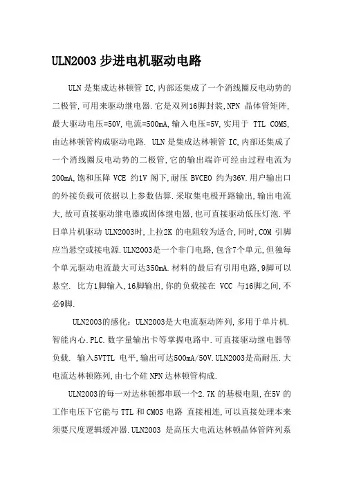
ULN2803A
DARLINGTON TRANSISTOR ARRAY
SLRS049E − FEBRUARY1997 − REVISED JULY 2006
1POST OFFICE BOX 655303 • DALLAS, TEXAS 75265D500-mA Rated Collector Current (Single
Output)
DHigh-Voltage Outputs...50V
DOutput Clamp Diodes
DInputs Compatible With Various Types of
Logic
DRelay Driver Applications
DCompatible with ULN2800A Series
description/ordering information
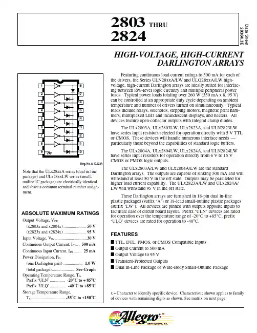
The ULN2803A is a high-voltage, high-current
Darlington transistor array. The device consists of
eight npn Darlington pairs that feature
high-voltage outputs with common-cathode
clamp diodes for switching inductive loads. The
collector-current rating of each Darlington pair is
500 mA. The Darlington pairs may be connected
in parallel for higher current capability.
Applications include relay drivers, hammer drivers, lamp drivers, display drivers (LED and gas discharge), line
drivers, and logic buffers. The ULN2803A has a 2.7-kΩ series base resistor for each Darlington pair for operation
directly with TTL or 5-V CMOS devices.
ORDERING INFORMATION
TAPACKAGE†ORDERABLE
PART NUMBERTOP-SIDE
MARKING
PDIP (N)Tube of 20ULN2803ANULN2803AN
°°Tube of 40ULN2803ADW−40C to 85CSOIC (DW)Reel of 2000ULN2803ADWRULN2803A
†Package drawings, standard packing quantities, thermal data, symbolization, and PCB design guidelines are
available at www.ti.com/sc/package.
Copyright 2006, Texas Instruments IncorporatedPlease be aware that an important notice concerning availability, standard warranty, and use in critical applications of
TexasInstruments semiconductor products and disclaimers thereto appears at the end of this data sheet.1
2
3
4
5
6
7
8
918
17
16
15
14
13
12
11
101B
2B
3B
4B
5B
6B
7B
8B
GND1C
2C
3C
4C
5C
6C
7C
8C
COMDW OR N PACKAGE
(TOP VIEW)
PRODUCTION DATA information is current as of publication date.Products conform to specifications per the terms of Texas Instrumentsstandard warranty. Production processing does not necessarily includetesting of all parameters.ULN2803A
DARLINGTON TRANSISTOR ARRAY
SLRS049E − FEBRUARY1997 − REVISED JULY 2006
2POST OFFICE BOX 655303 • DALLAS, TEXAS 75265logic diagram
8C7C6C5C4C3C2C
7654321
7B6B5B4B3B2B1B
11121314151617
COM88B
101C18
schematic (each Darlington pair)
2.7 kΩ
7.2 kΩ3 kΩCOM
Output C
EInput BULN2803A
DARLINGTON TRANSISTOR ARRAY
SLRS049E − FEBRUARY1997 − REVISED JULY 2006
3POST OFFICE BOX 655303 • DALLAS, TEXAS 75265absolute maximum ratings at 25°C free-air temperature (unless otherwise noted)†
Collector-emitter voltage 50 V. . . . . . . . . . . . . . . . . . . . . . . . . . . . . . . . . . . . . . . . . . . . . . . . . . . . . . . . . . . . . . . . . . .
Input voltage (see Note 1) 30 V. . . . . . . . . . . . . . . . . . . . . . . . . . . . . . . . . . . . . . . . . . . . . . . . . . . . . . . . . . . . . . . . . . .
Continuous collector current 500 mA. . . . . . . . . . . . . . . . . . . . . . . . . . . . . . . . . . . . . . . . . . . . . . . . . . . . . . . . . . . . . .
Output clamp diode current 500 mA. . . . . . . . . . . . . . . . . . . . . . . . . . . . . . . . . . . . . . . . . . . . . . . . . . . . . . . . . . . . . .
Total substrate-terminal current −2.5 A. . . . . . . . . . . . . . . . . . . . . . . . . . . . . . . . . . . . . . . . . . . . . . . . . . . . . . . . . . .
Package thermal impedance, θJA (see Notes 2 and 3):DW package 73.14°C/W. . . . . . . . . . . . . . . . . . . . . . .
N package 62.66°C/W. . . . . . . . . . . . . . . . . . . . . . . . .
Operating virtual junction temperature, TJ 150°C. . . . . . . . . . . . . . . . . . . . . . . . . . . . . . . . . . . . . . . . . . . . . . . . . . .
Storage temperature range, Tstg −65°C to 150°C. . . . . . . . . . . . . . . . . . . . . . . . . . . . . . . . . . . . . . . . . . . . . . . . . . .
†Stresses beyond those listed under “absolute maximum ratings” may cause permanent damage to the device. These are stress ratings only, and
functional operation of the device at these or any other conditions beyond those indicated under “recommended operating conditions” is not
implied. Exposure to absolute-maximum-rated conditions for extended periods may affect device reliability.
NOTES:1.All voltage values, unless otherwise noted, are with respect to the emitter/substrate terminal GND.
2.Maximum power dissipation is a function of TJ(max), θJA, and TA. The maximum allowable power dissipation at any allowable
ambient temperature is PD = (TJ(max) − TA)/θJA. Operating at the absolute maximum TJ of 150°C can affect reliability.
3.The package thermal impedance is calculated in accordance with JESD 51-7.
electrical characteristics at 25°C free-air temperature (unless otherwise noted)
PARAMETERTEST CONDITIONSMINTYPMAXUNIT
ICEXCollector cutoff currentVCE = 50 V,
See Figure 1II = 0,50µA