
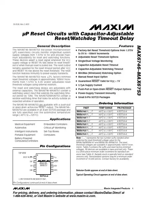
MAX6746KA46中文资料
- 格式:pdf
- 大小:186.51 KB
- 文档页数:14
Zowie Technology Corporation
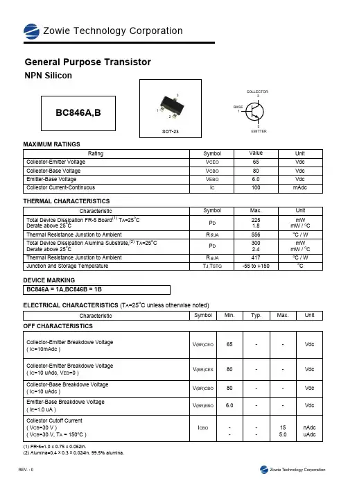
General Purpose TransistorNPN Silicon
BC846A,B1
21233
SOT-23
RatingSymbolValueUnit
CharacteristicCollector-Emitter VoltageVCEO65VdcCollector-Base VoltageVCBO80VdcEmitter-Base VoltageVEBO6.0VdcCollector Current-ContinuousIC100mAdc
CharacteristicSymbolMax.UnitTotal Device Dissipation FR-5 Board(1) TA=25oCDerate above 25oCPD2251.8mWmW / oC
Total Device Dissipation Alumina Substrate,(2) TA=25oCDerate above 25oCPD3002.4mWmW / oCThermal Resistance Junction to Ambient556oC / WMAXIMUM RATINGS
THERMAL CHARACTERISTICS
DEVICE MARKING
ELECTRICAL CHARACTERISTICS (TA=25oC unless otherwise noted)
OFF CHARACTERISTICSR JA
Thermal Resistance Junction to Ambient417oC / WR JAJunction and Storage Temperature
Collector-Emitter Breakdowe Voltage( IC=10 uAdc, VEB=0 )Collector-Base Breakdowe Voltage( IC=10 uAdc )Collector-Emitter Breakdowe Voltage( IC=10mAdc )
1 CD4046中文资料
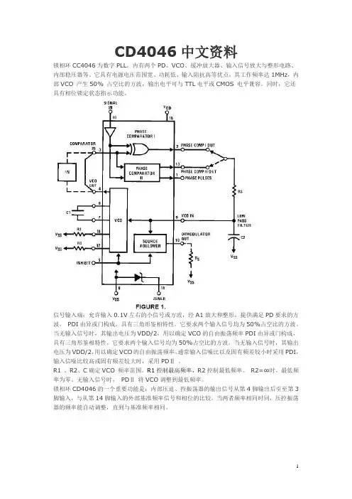
锁相环CC4046为数字PLL,内有两个PD、VCO、缓冲放大器、输入信号放大与整形电路、内部稳压器等。它具有电源电压范围宽、功耗低、输入阻抗高等优点,其工作频率达1MHz,内部VCO 产生50% 占空比的方波,输出电平可与TTL电平或CMOS 电平兼容。同时,它还具有相位锁定状态指示功能。
信号输入端:允许输入0.1V左右的小信号或方波,经A1放大和整形,提供满足PD要求的方波。 PDI由异或门构成,具有三角形鉴相特性。它要求两个输入信号均为50%占空比的方波。当无输入信号时,其输出电压为VDD/2,用以确定VCO的自由振荡频率PDI由异或门构成,具有三角形鉴相特性。它要求两个输入信号均为50%占空比的方波。当无输入信号时,其输出电压为VDD/2,用以确定VCO的自由振荡频率。通常输入信噪比以及固有频差较小时采用PDI,输入信噪比较高或固有频差较大时,采用PDⅡ 。
R1 、R2、C确定VCO 频率范围。R1控制最高频率,R2控制最低频率。 R2=∞时,最低频率为零。无输入信号时, PDⅡ 将VCO调整到最低频率。
锁相环CD4046的一个重要功能是:内部压迫、控振荡器的输出信号从第4脚输出后引至第3脚输入,与从第14脚输入的外部基准频率信号和相位的比较。当两者频率相同时同,压控振荡器的频率能自动调整,直到与基准频率相同。 2
CD4046引脚图
Absolute Maximum Ratings 绝对最大额定值:
DC Supply Voltage 直流供电电压 (VDD) −0.5 to +18 VDC
Input Voltage输入电压 (VIN) −0.5 to VDD +0.5 VDC
Storage Temperature Range储存温度范围 (TS) −65℃ to +150℃
Power Dissipation功耗 (PD)
SN54HCT645, SN74HCT645
OCTAL BUS TRANSCEIVERS
WITH 3ĆSTATE OUTPUTS
SCLS019D − MARCH 1984 − REVISED AUGUST 2003
1POST OFFICE BOX 655303 • DALLAS, TEXAS 75265DOperating Voltage Range of 4.5 V to 5.5 V
DHigh-Current 3-State Outputs Can Drive Up
To 15 LSTTL Loads
DLow Power Consumption, 80-µA Max ICCDTypical tpd = 14 nsD±6-mA Output Drive at 5 V
DLow Input Current of 1 µA Max
DInputs Are TTL-Voltage Compatible
DTrue Logic
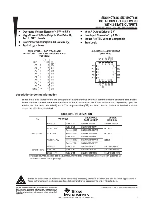
SN54HCT645...J OR W PACKAGE
SN74HCT645...DW, N, NS, OR PW PACKAGE
(TOP VIEW)SN54HCT645...FK PACKAGE
(TOP VIEW)
1
2
3
4
5
6
7
8
9
1020
19
18
17
16
15
14
13
12
11DIR
A1
A2
A3
A4
A5
A6
A7
A8
GNDVCC
OE
B1
B2
B3
B4
B5
B6
B7
B83212019
9101112134
5
6
7
818
17
16
15
14B1
B2
B3
B4
B5A3
A4
A5
A6
A7A2A1DIR
B7B6OE
A8
GNDB8VCC
description/ordering information
These octal bus transceivers are designed for asynchronous two-way communication between data buses.
These devices transmit data from the A bus to the B bus or from the B bus to the A bus, depending upon the

OBSOLETE
User'sGuide
SNVA116A–June2005–RevisedApril2013
AN-1385LM2746EvaluationBoard
1Introduction
Thisuser'sguidedescribestheTexasInstrumentsLM2746printedcircuitboard(PCB)designand
providesanexampletypicalapplicationcircuit.Thedemoboardallowscomponentdesignflexibilityin
ordertodemonstratetheversatilityoftheLM2746IC.
Thedemoboardcontainsavoltage-mode,high-speedsynchronousbuckregulatorcontroller.Thoughthe
controlsectionsoftheICareratedfor3to6V(VCC),thedriversectionsaredesignedtoacceptinput
supplyrails(VIN)ashighas16V.
Thedemoboarddesignregulatestoanoutputvoltageof1.2Vat3.5Awithaswitchingfrequencyof
1MHz.Note,thedemoboardisoptimizedfora1MHz,16Vinputvoltagecompensationdesign,ifaslower
switchingfrequencyandinputvoltageisdesired,pleaseconsultthedevicedatasheetforcontrolloop
compensationprocedures.Foradditionaldesignmodifications,refertotheDesignConsiderationsection