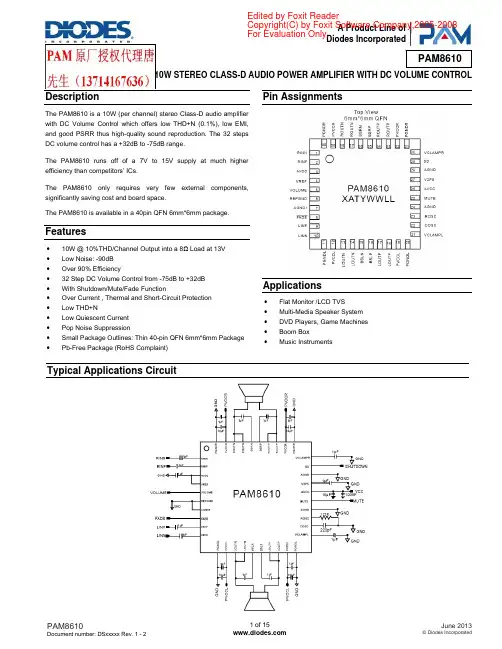
A Product Line ofDiodes Incorporated10W STEREO CLASS-D AUDIO POWER AMPLIFIER WITH DC VOLUME CONTROLDescriptionThe PAM8610 is a 10W (per channel) stereo Class-D audio amplifier with DC Volume Control which offers low THD+N (0.1%), low EMI, and good PSRR thus high-quality sound reproduction. The 32 steps DC volume control has a +32dB to -75dB range.The PAM8610 runs off of a 7V to 15V supply at much higher efficiency than competitors’ ICs.The PAM8610 only requires very few external components, significantly saving cost and board space.The PAM8610 is available in a 40pin QFN 6mm*6mm package.Features∙ 10W @ 10%THD/Channel Output into a 8Ω Load at 13V ∙ Low Noise: -90dB ∙ Over 90% Efficiency∙ 32 Step DC Volume Control from -75dB to +32dB ∙ With Shutdown/Mute/Fade Function ∙ Over Current , Thermal and Short-Circuit Protection ∙ Low THD+N∙ Low Quiescent Current ∙ Pop Noise Suppression∙ Small Package Outlines: Thin 40-pin QFN 6mm*6mm Package ∙Pb-Free Package (RoHS Complaint)Pin AssignmentsApplications∙ Flat Monitor /LCD TVS ∙ Multi-Media Speaker System ∙DVD Players, Game Machines∙ Boom Box ∙ Music InstrumentsTypical Applications CircuitEdited by Foxit ReaderCopyright(C) by Foxit Software Company,2005-2008For Evaluation Only.Pin DescriptionsFunctional Block DiagramAbsolute Maximum Ratings (@T A = +25°C, unless otherwise specified.)These are stress ratings only and functional operation is not implied. Exposure to absolute maximum ratings for prolonged time periods may affect device reliability. All voltages are with respect to ground.Recommended Operating Conditions(@T A = +25°C, unless otherwise specified.)Thermal InformationParameter PackageSymbolMaxUnitThermal Resistance (Junction to Ambient) QFN6mm*6mm θJA18.1°C/WThermal Resistance (Junction to Case) QFN6mm*6mm θJC7.6The Exposed PAD must be soldered to a thermal land on the PCB.Electrical Characteristics (@T A = +25°C, V DD = 12V, R L = 8Ω, unless otherwise specified.)Parameter Symbol TestConditions MinTypMaxUnits Supply Voltage V DD7.0 12 15 VContinuous Output Power P O THD+N = 0.1%, f = 1kHz, R L = 8Ω 5W THD+N = 1.0%, f = 1kHz, R L = 8Ω 8 THD+N = 10%, f = 1kHz, R L = 8Ω,V DD = 13V10 THD+N = 0.1%, f = 1kHz, R L = 4Ω (Note 3) 15Total Harmonic Distortion plus Noise THD+N P O = 5W, f = 1kHz, R L = 8Ω 0.1 % Quiescent Current I DD No Load 20 30 mA Supply Quiescent Current inShutdown Mode I SDShutdown = 0V 4 10 µADrain-Source On-State Resistance R DS(ON)V CC = 12VI O = 1AT J = +25°CHigh Side 200mΩLow Side 200Total 400Power Supply Ripple Rejection PSRR 1V PP Ripple, f = 1kHz,Inputs AC-Coupled to Ground-60 dBOscillator Frequency f OSC R OSC = 120kΩ, C OSC = 220pF 250 kHz Output Integrated Noise Floor VN 20Hz to 22kHz, A-Weighting -90 dB Crosstalk CS P O = 3W, R L = 8Ω, f = 1kHz -80 dBSignal to Noise Ratio SNR Maximum output at THD+N < 0.5%,f = 1kHz80 dBOutput Offset Voltage(measured differentially)|V OS| INN and INP connected together 30 mV 2.5V Bias Voltage V2P5 No Load 2.5 V Internal Analog Supply Voltage AV DD V DD = 7V to 15V 5.0 5.5 V Over Temperature Shutdown OTS 150 °C Thermal Hysteresis OTH 40 °CTypical Performance Characteristics (@T A = +25°C, V DD = 12V, R L = 8Ω, G V = 24dB, unless otherwise specified.)Typical Performance Characteristics (cont.) (@T A = +25°C, V DD = 12V, R L = 4Ω, G V = 24dB, unless otherwise specified.)Typical Performance Characteristics (cont.) (@T A = +25°C, V DD = 12V, R L = 8Ω, G V = 24dB, unless otherwise specified.)Typical Performance Characteristics (cont.) (@T A = +25°C, V DD = 12V, R L = 8Ω, G V = 24dB, unless otherwise specified.)Notes: PCB information for power dissipation measurement.1. The PCB size is 74mm 68mm with 1.2mm thickness, two layers and Fr4.2. 16 vias at the thermal land on the PCB with 0.5mm diameter.3. The size of exposed copper is 10mm*10mm with 3oz thickness.Application InformationTest Setup for Performance TestingNotes: 4. The AP AUX-0025 low pass filter is necessary for class-D amplifier measurement with AP analyzer.5. Two 22μH inductors are used in series with load resistor to emulate the small speaker for efficiency measurement.Power and Heat DissipationChoose speakers that are able to stand large output power from the PAM8610. Otherwise, speaker may suffer damage.Heat dissipation is very important when the device works in full power operation. Two factors affect the heat dissipation, the efficiency of the device that determines the dissipation power, and the thermal resistance of the package that determines the heat dissipation capability.In operation, some of power is dissipated to the resistors.Power Dissipation: P LOSS = (P O*(1-η/η)*2The PAM8610’s efficiency is 90% with 10W ouput and 8Ω load. The dissipation power is 2.22W.Thermal resistance of junction to ambient of the QFN package is 18.1°C/W and the junction temperature T J = P LOSS * θJA+T A, where T A is ambient temperature. If the ambient temperature is +85°C, the QFN’s junction temperatureT J = 2.22*18.1 + 85 = +125°Cwhich is lower than +150°C rated junction temperature.If the rated workable junction temperature is 150°C, the relat ionship between ambient temperature and permitted P LOSS is shown in below diagram.From the diagram, it can be found that when the device works at 10W/8Ω load the dissipation power is 1.1W per channel, 2.2W total, the permitted ambient temperature is over 100°C. This is proven by actual test. The PAM8610 can work in full output power under +85°C ambient temperature.Application Information (cont.)Heat Dissipation in PCB DesignGenerally, class-D amplifiers are high efficiency and need no heat sink. For high power ones that has high dissipation power, the heat sink may also not necessary if the PCB is carefully designed to achieve good heat by the PCB itself.Dual-Side PCBTo achieve good heat, the PCB’s copper plate should be thicker than 0.035mm and both sides of the PCB should be utilized for heat sink.The thermal pad on the bottom of the device should be soldered to the plate of the PCB, and via holes, usually 9 to 16, should be drilled in the PCB area under the device and deposited copper on the vias should be thick enough so that the heat can be dissipated to the other side of the plate. There should be no insulation mask on the other side of the copper plate. It is better to drill more vias around the device if possible.4-Layer PCBIf it is 4-layer PCB, the two middle layers of grounding and power can be employed for heat dissipation, isolating them into serval islands to avoid short between ground and power.Consideration for EMIFilters are not required if the traces from the amplifier to the speakers are short (<20cm). But most applications require a ferrite bead filter as shown in below figure. The ferrite bead filter reduces EMI of around 1MHz and higher to meet the FCC and CE's requirements. It is recommended to use a ferrite bead with very low impedances at low f requenc ies and high impedance at high frequencies (above 1MHz).The EMI characteristics are as follows after employing the ferrite bead.Application Information (cont.)Volume ControlA DC volume control section is integrated in PAM8610, controlling via V REF, VOLUME and V REFGND terminals. The voltage on VOLUME pin, without exceeding V REF, determines internal amplifier gain as listed in Table 1.If a resistor divider is used to fix gain of the amplifier, the V REF terminal can be directly connected to AV DD and the resistor divider connected across V REF and REFGND. For fixed gain, the resistor divider values are to center the voltage given in the Table 1.FADE OperationThe FADE terminal is a logic input that controls the operation of the volume control circuitry during transitions to and from the shutdown state and during power-up.A logic low on this terminal will set the amplifier in fade mode. During power-up or recovery from the shutdown state (a logic high is applied to the SD terminal), the volume is smoothly ramped up from the mute state, -75dB, to the desired volume set by the voltage on the volume control terminal. Conversely, the volume is smoothly ramped down from the current state to the mute state when a logic low is applied to the SD terminal. A logic high on this pin disables the volume fade effect during transitions to and from the shutdown state and during power-up. During power-up or recovery from the shutdown state (a logic high is applied to the SD terminal), the transition from the mute state, -75dB, to the desired volume setting is less than 1ms. Conversely, the volume ramps down from current state to the mute state within 1ms when a logic low is applied to the SD terminal.MUTE OperationThe MUTE pin is an input for controlling the output state of the PAM8610. A logic high on this pin disables the outputs and low enables the outputs. This pin may be used as a quick disable or enable of the outputs without a volume fade.For power saving, the SD pin should be used to reduce the quiescent current to the absolute minimum level. The volume will fade, increasing or decreasing slowly, when leaving or entering the shutdown state if the FADE terminal is held low. If the FADE terminal is held high, the outputs will transit very quickly. Refer to the FADE operation section.Shutdown OperationThe PAM8610 employs a shutdown operation mode to reduce supply current to the absolute minimum level during periods of non-use to save power. The SD input terminal should be held high during normal operation when the amplifier is in use. Pulling SD low causes the outputs to mute and the amplifier to enter a low-current state. SD should never be left unconnected to prevent the amplifier from unpredictable operation.For the best power-off pop performance, the amplifier should be set in shutdown mode prior to removing the power supply voltage.Internal 2.5V Bias Generator Capacitor SelectionThe internal 2.5V bias generator (V2P5) provides the internal bias for the preamplifier stage. The external input capacitors and this internal reference allow the inputs to be biased within the optimal common-mode range of the input preamplifiers.The selection of the capacitor value on the V2P5 terminal is critical for achieving the best device performance. During startup or recovery from shutdown state, the V2P5 capacitor determines the rate at which the amplifier starts up. When the voltage on the V2P5 capacitor equals 0.75 x V2P5, or 75% of its final value, the device turns on and the Class-D outputs start switching. The startup time is not critical for the best de-pop performance since any heard pop sound is the result of the Class-D output switching-on other than that of the startup time. However, at least a 0.47μF capacitor is recommended for the V2P5 capacitor.Another function of the V2P5 capacitor is to filter high frequency noise on the internal 2.5V bias generator.Power Supply Decoupling, C SThe PAM8610 is a high-performance CMOS audio amplifier that requires adequate power supply decoupling to ensure the output total harmonic distortion (THD) as low as possible. Power supply decoupling also prevents oscillations caused by long lead between the amplifier and the speaker. The optimum decoupling is achieved by using two capacitors of different types that target different types of noise on the power supply leads. For higher frequency transients, spikes, or digital hash on the line, a good low equivalent-seriesresistance(ESR) ceramic capacitor, typically 1μF, is recommended, placing as close as possible to the device’s V CC lead. To filter lower-frequency noises, a large aluminum electrolytic capacitor of 10μF or greater is recommended, placing near the audio power amplifier. The 10μF capacitor also serves as a local storage capacitor for supplying current during large signal transients on the amplifier outputs.Application Information (cont.)Selection of COSC and ROSCThe switching frequency is determined by the values of components connected to R OSC (pin 23) and C OSC (pin 22) and calculated as follows:f OSC = 2π/ (R OSC * C OSC)The frequency may varies from 225kHz to 275kHz by adjusting the values of R OSC and C OSC. The recommended values are C OSC = 220pF, R OSC = 120kΩ for a switching frequency of 250kHz.BSN and BSP CapacitorsThe full H-bridge output stages use NMOS transistors only. They therefore require bootstrap capacitors for the high side of each output to turn on correctly. At least 220nF ceramic capacitor, rated for at least 25V, must be connected from each output to its corresponding bootstrap input. Specifically, one 220nF capacitor must be connected from xOUTP to xBSP, and another 220nF capacitor from xOUTN to xBSN. It is recommended to use 1µF BST capacitor to replace 220nF (pin15, pin 16, pin 35 and pin 36) for lower than 100Hz applications.VCLAMP CapacitorsTo ensure that the maximum gate-to-source voltage for the NMOS output transistors not exceeded, two internal regulators are used to clamp the gate voltage. Two 1μF capacitors must be connected from VCLAMPL and VCLAMPR to ground and must be rated for at least 25V. The voltagesat the VCLAMP terminals vary with V CC and may not be used to power any other circuitry.Internal Regulated 5-V Supply (AVDD)The AVDD terminal is the output of an internally generated 5V supply, used for the oscillator, preamplifier, and volume control circuitry. It requires a 0.1μF to 1μF capacitor, placed very close to the pin to ground to keep the regulator stable. The regulator may not be used to power any external circuitry.Differential InputThe differential input stage of the amplifier eliminates noises that appear on the two input lines of the channel. To use the PAM8610 with a differential source, connect the positive lead of the audio source to the INP input and the negative lead from the audio source to the INN input. To use the PAM8610 with a single-ended source, acground the INP input through a capacitor equal in value to the input capacitor on INN and apply the audio source to the INN input. In a single-ended input application, the INP input should be acgrounded at the audio source other than at the device input for best noise performance.Using Low-ESR CapacitorsLow- ESR capacitors are recommended throughout this application section. A real (with respect to ideal) capacitor can be modeled simply as a resistor in series with an ideal capacitor. The voltage drop across this resistor minimizes the beneficial effects of the capacitor in the circuit. The lower the equivalent value of this resistance the more the real capacitor behaves as an ideal capacitor.Short-Circuit ProtectionThe PAM8610 has short circuit protection circuitry on the outputs to prevent damage to the device when output-to-output shorts, output-to-GND shorts, or output-to-V CC shorts occur. Once a short-circuit is detected on the outputs, the output drive is immediately disabled. This is a latched fault and must be reset by cycling the voltage on SD the pin to a logic low and back to the logic high state for normal operation. This will clear the short-circuit flag and allow for normal operation if the short was removed. If the short was not removed, the protection circuitry will again activate.Thermal ProtectionThermal protection on the PAM8610 prevents damage to the device when the internal die temperature exceeds +150°C. There is a ±15 degree tolerance on this trip point from device to device. Once the die temperature exceeds the set thermal point, the device enters into the shutdown state and the outputs are disabled. This is not a latched fault. The thermal fault is cleared once the temperature of the die is reduced by 40°C. The device begins normal operation at this point without external system intervention.Ordering InformationPart Number Part Marking Package TypeStandard PackagePAM8610TRPAM8610XATYWWLLQFN6x6-40 2500 Units/Tape&ReelMarking InformationPackage Outline Dimensions (All dimensions in mm.) QFN6x6-40IMPORTANT NOTICEDIODES INCORPORATED MAKES NO WARRANTY OF ANY KIND, EXPRESS OR IMPLIED, WITH REGARDS TO THIS DOCUMENT, INCLUDING, BUT NOT LIMITED TO, THE IMPLIED WARRANTIES OF MERCHANTABILITY AND FITNESS FOR A PARTICULAR PURPOSE (AND THEIR EQUIVALENTS UNDER THE LAWS OF ANY JURISDICTION).Diodes Incorporated and its subsidiaries reserve the right to make modifications, enhancements, improvements, corrections or other changes without further notice to this document and any product described herein. Diodes Incorporated does not assume any liability arising out of the application or use of this document or any product described herein; neither does Diodes Incorporated convey any license under its patent or trademark rights, nor the rights of others. Any Customer or user of this document or products described herein in such applications shall assume all risks of such use and will agree to hold Diodes Incorporated and all the companies whose products are represented on Diodes Incorporated website, harmless against all damages.Diodes Incorporated does not warrant or accept any liability whatsoever in respect of any products purchased through unauthorized sales channel. Should Customers purchase or use Diodes Incorporated products for any unintended or unauthorized application, Customers shall indemnify and hold Diodes Incorporated and its representatives harmless against all claims, damages, expenses, and attorney fees arising out of, directly or indirectly, any claim of personal injury or death associated with such unintended or unauthorized application.Products described herein may be covered by one or more United States, international or foreign patents pending. Product names and markings noted herein may also be covered by one or more United States, international or foreign trademarks.This document is written in English but may be translated into multiple languages for reference. Only the English version of this document is the final and determinative format released by Diodes Incorporated.LIFE SUPPORTDiodes Incorporated products are specifically not authorized for use as critical components in life support devices or systems without the express written approval of the Chief Executive Officer of Diodes Incorporated. As used herein:A. Life support devices or systems are devices or systems which:1. are intended to implant into the body, or2. support or sustain life and whose failure to perform when properly used in accordance with instructions for use provided in thelabeling can be reasonably expected to result in significant injury to the user.B. A critical component is any component in a life support device or system whose failure to perform can be reasonably expected to cause thefailure of the life support device or to affect its safety or effectiveness.Customers represent that they have all necessary expertise in the safety and regulatory ramifications of their life support devices or systems, and acknowledge and agree that they are solely responsible for all legal, regulatory and safety-related requirements concerning their products and any use of Diodes Incorporated products in such safety-critical, life support devices or systems, notwithstanding any devices- or systems-related information or support that may be provided by Diodes Incorporated. Further, Customers must fully indemnify Diodes Incorporated and its representatives against any damages arising out of the use of Diodes Incorporated products in such safety-critical, life support devices or systems.Copyright © 2012, Diodes Incorporated。