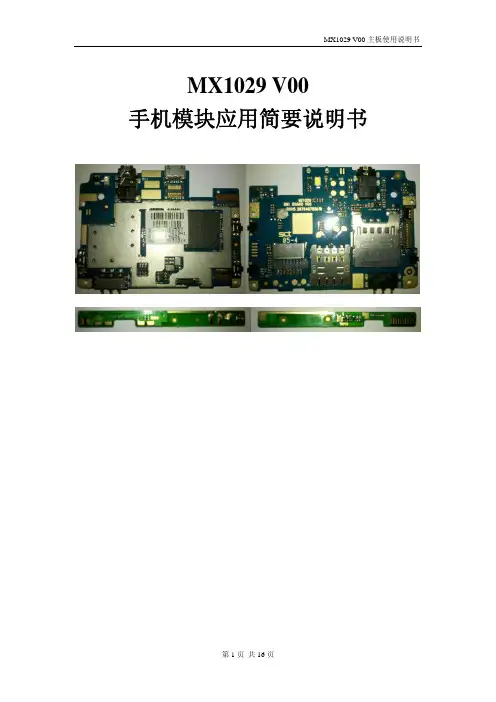
LY1029规格书 输出可调
- 格式:pdf
- 大小:2.10 MB
- 文档页数:13
ULTRA-SMALL PACKAGE PWM/PFM SWITCHING CONTROL
ULTRA-SMALL PACKAGE PWM/PFM SWITCHING CONTROL STEP-UP SWITCHING REGULATOR
Description:
The LY1029 series is a CMOS step-up switching regulator which mainly consists of a reference voltage source, an oscillation circuit, an error amplifier, a phase compensation circuit, a PWM/PFM switching control circuit. With an external low-ON-resistance Nch Power MOS, this product is applicable to applications requiring high efficiency and high output current. The LY1029 series switches its operation to the PFM control circuit whose duty ratio is 15 % with to the PWM/PFM switching control circuit under a light load and to prevent decline in the efficiency by IC operation current.
Pin Name
FB VDD CE GND
5
EXT
Function
Feed Back voltage pin IC power supply pin Shutdown pin GND pin External transistor connection pin
Tel:(86)0755-82985079
-
-
Operation holding voltage
VHLD
IOUT=1mA,Measured by decreasing VIN voltage gradually
0.7
-
Current consumption 1 ISS1 VFB=VFB(S)× 0.95-
-
100
Current consumption 2 ISS2 VFB=1.5V
SYMBOL VDD EXT VOUT VCE IEXT Pd TOpr Tstg
RATINGS -0.3~6.5 -0.3~VDD+0.3 -0.3~6.5 -0.3~Vin+0.3
±1000 250
-25~+85 -40~+125
UNITS V V V V mA
mW
℃
℃
Tel:(86)0755-82985079 13530003715
Ta=-25—85℃
-
±50
Oscillation frequency
fosc
-
255
300
Max. duty ratio
MAXDUTY VFB=VFB(S)× 0.95
-
78
PWM/PFM switching duty ratio
PFMDUTY VFB=VFB(S)× 1.5, no load
-
15
ISS1 VOUT=VOUT(S)× 0.95
-
200
-
uA
2
Current consumption 2
ISS2 VOUT=VOUT(S)+0.5V
-20ຫໍສະໝຸດ -uA2Current consumption during shutdown
ISSS VCE=0V
-
0.1
0.5
uA
2
EXT pin output current
CE FUNCTION
Yes
Yes
VDD FUNCTION
Yes
Yes
FB FUNCTION
No
Yes
FEATURES
Ext + CE Ext +FB
Pin Configuration:
Pin information:
SOT-23-5
LY1029Dxx :
Pin Number SOT-23-5 1 2 3 4
13530003715
2/13
Block Diagram:
Absolute Maximum Rang:
PARAMETER VDD Pin Voltage EXT Pin Voltage VOUT Pin Voltage CE Pin Voltage EXT Pin Voltage Power Dissipation (SOT-23-5) OperatingTemperature Range StorageTemperature Range
Tel:(86)0755-82985079 13530003715
4/13
LY1029F
Measuring conditions:VDD=VVCE=3.3V,Topt=25℃。Unless otherwise specified。
Parameter Feed back voltage
-
15
Current consumption during shutdown
ISSS VCE=0V
-
0.01
EXT pin output current
IEXTH VEXT=VOUT-0.4V IEXTL VEXT=0.4V
-
-25
-
40
Feed back voltage temperature coefficient
1.8V≦VDD<6V is recommended to stabilize the output voltage and oscillation frequency.
VST2
No external parts, voltage applied to VOUT
-
-
0.7
V
1
Operation holding voltage
VHLD
IOUT=1mA , Measured by decreasing VIN voltage gradually
0.7
-
-
V
2
Current consumption 1
Pin Name
VOUT VDD CE GND
5
EXT
Function
Output voltage pin IC power supply pin
Shutdown pin GND pin
External transistor connection pin
LY1029F :
Pin Number SOT-23-5 1 2 3 4
VSH Measured the oscillation at EXT pin
0.75
-
Shutdown pin input voltage
VSL1 Judged the stop of VOUT≥1.5V
-
-
oscillation at EXT
VSL2 pin
VOUT<1.5V
-
-
Shutdown pin input voltage
SYMBOL VOUT
CONDITIONS -
MIN TYP
MAX UNITS CIRCUIT
VOUT(S)X 0.98
VOUT(S)
VOUT(S)X 1.02
V
2
Input voltage
VIN
-
-
-
6
V
2
Operation start voltage
VST1 IOUT=1mA
-
-
0.9
V
2
Oscillation start voltage
ISH VCE=VFB(S)×0.95 ISL VCE=0V
-0.1
-
-0.1
-
Soft start time
tss
-
-
2
Efficiency
EFFI
-
-
85
1. VOUT(S) is the set output voltage value,and VOUT is the typital value of the output voltage. 2. VOUT(S) can be set by using the rate of VFB and output voltage setting resisitors(R1,R2). 3. VFB(S) is the set output voltage value. 4. VDD/VOUT separate type:
IEXTH IEXTL
VEXT=VOUT-0.4V VEXT=0.4V
-
-35
-
mA
2
-
55
-
mA
2
Line regulation
△VOUT1 VIN=VOUT(S)×0.4~×0.6
-
30
-
mV
2
Load regulation
△VOUT2 IOUT=10uA~VOUT/50×1.25
-
35
-
mV
2
VSL2
VOUT<1.5V
-
-
-
V
1
0.3
ULTRA-SMALL PACKAGE PWM/PFM SWITCHING CONTROL STEP-UP SWITCHING REGULATOR
Description:
The LY1029 series is a CMOS step-up switching regulator which mainly consists of a reference voltage source, an oscillation circuit, an error amplifier, a phase compensation circuit, a PWM/PFM switching control circuit. With an external low-ON-resistance Nch Power MOS, this product is applicable to applications requiring high efficiency and high output current. The LY1029 series switches its operation to the PFM control circuit whose duty ratio is 15 % with to the PWM/PFM switching control circuit under a light load and to prevent decline in the efficiency by IC operation current.
Pin Name
FB VDD CE GND
5
EXT
Function
Feed Back voltage pin IC power supply pin Shutdown pin GND pin External transistor connection pin
Tel:(86)0755-82985079
-
-
Operation holding voltage
VHLD
IOUT=1mA,Measured by decreasing VIN voltage gradually
0.7
-
Current consumption 1 ISS1 VFB=VFB(S)× 0.95-
-
100
Current consumption 2 ISS2 VFB=1.5V
SYMBOL VDD EXT VOUT VCE IEXT Pd TOpr Tstg
RATINGS -0.3~6.5 -0.3~VDD+0.3 -0.3~6.5 -0.3~Vin+0.3
±1000 250
-25~+85 -40~+125
UNITS V V V V mA
mW
℃
℃
Tel:(86)0755-82985079 13530003715
Ta=-25—85℃
-
±50
Oscillation frequency
fosc
-
255
300
Max. duty ratio
MAXDUTY VFB=VFB(S)× 0.95
-
78
PWM/PFM switching duty ratio
PFMDUTY VFB=VFB(S)× 1.5, no load
-
15
ISS1 VOUT=VOUT(S)× 0.95
-
200
-
uA
2
Current consumption 2
ISS2 VOUT=VOUT(S)+0.5V
-20ຫໍສະໝຸດ -uA2Current consumption during shutdown
ISSS VCE=0V
-
0.1
0.5
uA
2
EXT pin output current
CE FUNCTION
Yes
Yes
VDD FUNCTION
Yes
Yes
FB FUNCTION
No
Yes
FEATURES
Ext + CE Ext +FB
Pin Configuration:
Pin information:
SOT-23-5
LY1029Dxx :
Pin Number SOT-23-5 1 2 3 4
13530003715
2/13
Block Diagram:
Absolute Maximum Rang:
PARAMETER VDD Pin Voltage EXT Pin Voltage VOUT Pin Voltage CE Pin Voltage EXT Pin Voltage Power Dissipation (SOT-23-5) OperatingTemperature Range StorageTemperature Range
Tel:(86)0755-82985079 13530003715
4/13
LY1029F
Measuring conditions:VDD=VVCE=3.3V,Topt=25℃。Unless otherwise specified。
Parameter Feed back voltage
-
15
Current consumption during shutdown
ISSS VCE=0V
-
0.01
EXT pin output current
IEXTH VEXT=VOUT-0.4V IEXTL VEXT=0.4V
-
-25
-
40
Feed back voltage temperature coefficient
1.8V≦VDD<6V is recommended to stabilize the output voltage and oscillation frequency.
VST2
No external parts, voltage applied to VOUT
-
-
0.7
V
1
Operation holding voltage
VHLD
IOUT=1mA , Measured by decreasing VIN voltage gradually
0.7
-
-
V
2
Current consumption 1
Pin Name
VOUT VDD CE GND
5
EXT
Function
Output voltage pin IC power supply pin
Shutdown pin GND pin
External transistor connection pin
LY1029F :
Pin Number SOT-23-5 1 2 3 4
VSH Measured the oscillation at EXT pin
0.75
-
Shutdown pin input voltage
VSL1 Judged the stop of VOUT≥1.5V
-
-
oscillation at EXT
VSL2 pin
VOUT<1.5V
-
-
Shutdown pin input voltage
SYMBOL VOUT
CONDITIONS -
MIN TYP
MAX UNITS CIRCUIT
VOUT(S)X 0.98
VOUT(S)
VOUT(S)X 1.02
V
2
Input voltage
VIN
-
-
-
6
V
2
Operation start voltage
VST1 IOUT=1mA
-
-
0.9
V
2
Oscillation start voltage
ISH VCE=VFB(S)×0.95 ISL VCE=0V
-0.1
-
-0.1
-
Soft start time
tss
-
-
2
Efficiency
EFFI
-
-
85
1. VOUT(S) is the set output voltage value,and VOUT is the typital value of the output voltage. 2. VOUT(S) can be set by using the rate of VFB and output voltage setting resisitors(R1,R2). 3. VFB(S) is the set output voltage value. 4. VDD/VOUT separate type:
IEXTH IEXTL
VEXT=VOUT-0.4V VEXT=0.4V
-
-35
-
mA
2
-
55
-
mA
2
Line regulation
△VOUT1 VIN=VOUT(S)×0.4~×0.6
-
30
-
mV
2
Load regulation
△VOUT2 IOUT=10uA~VOUT/50×1.25
-
35
-
mV
2
VSL2
VOUT<1.5V
-
-
-
V
1
0.3