Electroplating Solder Bumping Flip Chip Technology
- 格式:ppt
- 大小:3.74 MB
- 文档页数:21

系统级封装技术(SiP)引领封测 产业的 混搭 潮 产业的“混搭”潮2010年6月25号混搭英文原词为Mix and Match。
混搭是一个时尚界专用名词,指将不同 风格,不同材质,不同身价的东西按照个人口味拼凑在 起,从而混合 风格,不同材质,不同身价的东西按照个人口味拼凑在一起,从而混合 搭配出完全个人化的风格,就是不要规规矩矩,是一种时髦,但决不能 等同于胡穿乱配的毫无章法。
混搭最典型的莫过于韩式混搭,韩国街头流行起一种更实用,更有味道 的混搭新哲学。
穿出层次,叠穿法则是混搭哲学中最基础课程,其中最 奏 重要的是搭配的节奏感,这也正是混搭风能在当今流行的重要原因。
系统级封装技术的特点非常符合和“混搭”的精髓,有一 脉相承 异曲同工之处 脉相承、异曲同工之处内容1、系统级封装的发展背景 2、系统级封装的定义 系统级封装的定义 3、系统级封装的优势 系统级封装的优势 4、系统级封装的成本 5、长电科技系统级封装技术及服务的介绍 6、长电科技系统级封装产品及应用 长电科技系统级封装产品及应用 7、总结1、系统级封装的发展背景¾当今社会,电子系统的发展趋势是小型化、高性能、多功能、高 可靠性和低成本,在这些需求的强力驱动下,电子产品的演进速度 超乎寻常 ¾在物联网、移动支付、移动电视、移动互联网、3G通讯等新生应 用的引导下,一大批新型电子产品孕育而生 ¾目前系统级封装产品在计算机、汽车电子、医疗电子、军事电子、 消费类电子(手机 蓝牙 消费类电子(手机、蓝牙、Wi-Fi、交换机等)等领域内都有巨大 交换机等)等领域内都有巨大 的市场 ¾系统级芯片(System 系统级芯片(S t on Chip, Chi SoC)的发展随着摩尔定律的脚 S C)的发展随着摩尔定律的脚 步不断演进,然而随着SoC发展至深次微米以下先进制程世代后, 已经面临极大的技术发展瓶颈,SoC已难面面俱到。

Available Flip Chip TutorialsTutorial 1. Introduction to Flip ChipTutorial 2. Solder Bump Flip ChipTutorial 3. Stud Bump Flip ChipTutorial 4. Polymer Bump Flip ChipTutorial 5. Anisotropic Conductive Film (ACF)Flip ChipTutorial 6. A Brief History of Flipped ChipsTutorial 7. Electroless Nickel-Gold Flip ChipTutorial 8. Reworking Underfilled Flip ChipTutorial 9. Thermosonic Flip Chip AssemblyTutorial 10. Flip Chip Interconnection for Detector ArraysTutorial 11. Under Bump Metallization (UBM)Tutorial 12. Solder Bumping Step by StepTutorial 14. Bonding Edge Emitting Laser Diodes Using Gold/Tin Preforms Tutorial 15. Substrates for Flip ChipTutorial 16. Packaging, Handling, and Storing of Solder SpheresTutorial 17. SOC, SOP, and WLSCPTutorial 18. Fluxing for Flip ChipTutorial 20. Causes of MisalignmentTutorial 21. Probing Bumped Flip ChipsTutorial 22. Controlling Stress in Thin FilmsTutorial 23. Reworking Anisotropic Conductive Film (ACF) Flip Chip AssembliesTutorial 24. Gold Stud Bump ApplicationsTutorial 25. Low Temperature Flip Chip for Flexible DisplaysTutorial 26. The Coming of Copper UBMTutorial 27. Shaping Gold Ball BumpsTutorial 28. Copper Bumps for Flip Chip AssemblyTutorial 29. Micro-Posts: Tall, Slender, Stud Bumps.Tutorial 30. Measuring thin films by spectral reflectance, Part 1Tutorial 31. Wafer level hermetic cavity chip scale packages for RFTutorial 32. Gold Stud Bumping - the Other Flip-Chip ProcessTutorial 33. Conductive Polymer Assembly of High Pin Count Flip Chip Tutorial 34. Sputtered nickel UBM for lead-free solder bumpingTutorial 35. Measuring thin films by spectral reflectance, Part 2Tutorial 36. MEMS Special Packaging NeedsTutorial 37. Too much gold can be a bad thing.Tutorial 38. Evaporated Indium Bumps for Flip ChipTutorial 39. Electromigration and Thermomigration in Flip Chip Solder Joints Tutorial 40. Nano-embossing reaches production.Tutorial 41. Hermeticity: much to do about nothing.Tutorial 42. Evaluating Wafer Level Solder Reflow Options to Maximize Yield Tutorial 43. Wafer-level Hermetic Cavity Packaging.Tutorial 44. Advanced Wafer-level Cleaning Method.Tutorial 45. Lead-Free Facts and Myths.Tutorial 46. Alloy Electroplating: The best solution for Au-Sn solder?Tutorial 47. Flip Chip Bonder for Assembling 3D MEMSTutorial 48. Drop-in Lead-free solderTutorial 49. Wafer-level Nano-opticsTutorial 50. Gold Stud Bump UpdateTutorial 51. Solder Bumping Single DieTutorial 52. New Generation Nano-Imprint Lithography System Tutorial 53. Probe testing differences in lead-free bumpsTutorial 54. Nano Particle AdhesivesTutorial 55. The Promise of C4NPTutorial 56. Injection Molding Solder BumpsTutorial 57. Thermosonic Bonding of 1,000-bump Flip ChipsTutorial 58. Nanosoldering electronic components at room temperature Tutorial 59. Lower temperature lead-free flip chipTutorial 60. Nanotube Heat SinksTutorial 61. Lead-Free Solder Bumping MethodsTutorial 62. Vapor Jet Deposition of Multi-Metal FilmsTutorial 63. C4NP Test DataTutorial 64. Silver Nano-platelet Precursors for Ultra-Thin Conductors Tutorial 65. Cleaning microelectronic devices by Vacuum Cavitational StreamingTutorial 66. The Folly of RoHSTutorial 67. Underfilling ProcessesTutorial 68. Plasma pretreatment of Flip Chip and CSP assemblies Tutorial 69. Resonance Sensor Technology for Bump InspectionTutorial 70. Controlled-expansion substrates for WLP Tutorial 71. Nailing ICs TogetherTutorial 72. Redistribution LayersTutorial 73. Advanced ReworkTutorial 74. High Conductivity Nickel-Fiber ACF Tutorial 75. Unique Polished Polyimide Substrate Tutorial 76. Jet Dispensing of UnderfillsTutorial 77. Solderless Copper AssemblyTutorial 78. Quilt PackagingTutorial 79. Bump CoolingTutorial 80. Nano-particle Solder PasteTutorial 81. Wafer-level CSP with Integrated Passives Tutorial 82. Putting Photons on the ChipTutorial 83. Soldering Stud BumpsTutorial 84. Avoiding Lead-Free Brittle Fractures Tutorial 85. Chip to Wafer Hermetic Cavity Sealing Tutorial 86. 3D Silicon ChipsTutorial 87. Laminated Chip PackagesTutorial 88. ElectroChemical Pattern Replication。
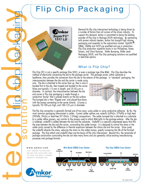
ologyDemand for flip chip interconnect technology is being driven bya number of factors from all corners of the silicon industry. Tosupport this demand, Amkor is committed to being the leadingprovider of Flip Chip in Package (FCiP) technology. By partneringwith proven industry leaders, Amkor has brought high volumepackaging and assembly to the subcontract market.fc BGA,Flip Chip production capability exists in our Philippines, Korea,Taiwan, and China factories. Wafer Bumping, Wafer LevelPackaging (WLP), and Flip Chip packaging solutions are qualifiedin lead-free options.What is Flip Chip?Flip Chip (FC) is not a specific package (like SOIC), or even a package type (like BGA). Flip Chip describes thebonded first to the die, then looped and bonded to the carrier.tReduced signal inductance - because the interconnect is MUCH shorter in length (0.1 mm vs 1-5 mm),the inductance of the signal path is greatly reduced. This is a key factor in high speed communicationReduced power/ground inductance - by using flip chip interconnect, power can be brought directly intothe core of the die, rather than having to be routed to the edges. This greatly decreases the noise of theHigher signal density - the entire surface of the die can be used for interconnect, rather than just theedges. This is similar to the comparison between QFP and BGA packages. Because flip chipReduced package footprint - in some cases, the total package size can be reduced usingflip chip. This can be achieved by either reducing the die to package edge requirements, sinceno extra space is required for wires, or in utilizing higher density substrate technology, which allows for reducedfocused on specific benefits that serve a given market. Amkor offers the widest possible range of flip chip packaging solutions to meet the diverse needs of customers and end users. Combining their extensive manufacturing knowledge with all types of packaging interposers and further leveraging their leadership role in flip chip interconnect technology, Amkor continues to pursue new package solutions. This kind of focus is essential to insure that as new market needs emerge requiring flip chip interconnect, Amkor is ready with the optimumCurrent Package Options:Super FC®Package:Amkor Technology is now offering Super FC® packaging, the super performance flip chip solution. Flip chip interconnect utilizes array interconnect of die to substrate as a replacement for conventional wire bonding. This allows the entire die surface to be used for electrical connections to the substrate, exponentially increasing the I/O per unit area vs. perimeter interconnect technologies. Implementing process technology licensed from industry leader LSI Logic, Amkor’s Supe rFC package uses solder bump flip chip interconnect, and can route over 1000 signal traces from a single die out to a 1.0 mm pitch BGA footprint.Supe rFC packages are assembled around state-of-the-art laminate substrates. Utilizing multi-layer, blind and buried vias, laser drilled build-up structures, and ultra fine line/space metallization, Supe rFC has the highest routing density BGA available. Using flip chip interconnect automatically improves package electrical performance by removing the high inductance wires and replacing them with low inductance solder connections. By combining flip chip with ultra advanced substrate technology, packages can be electrically tuned for maximum electrical performance.Features:•4-10 layer build up substrates using epoxy laminate•Target Market - Internet Workstation Processors, High Bandwidth System Communications Devices•Variety of heatspreader options, passive attach•175 µm minimum bump pitch•Die sizes up to 16.7 mm, extending to 21 mm•Package sizes from 27 mm to 50 mm, passive attach•JEDEC MS-034 compliant, 1.0 mm pitch BGA footprint•Package solutions up to 2400 ballsfc Ceramic CBGA/CLGA/CLLGA/Solder Column Interposer:Flip chip packaging solution for most of flip chip's history.Features:•5-20 layers, Alumina and HiTCE•Target Market - Internet Workstation Processors, High Bandwidth System Communications Devices, Printer Applications•Lidded and unlidded versions, LGA and BGA, Solder Column Interposer, Passive Attach•200 µm minimum bump pitch•Die sizes up to 21 mm•Package sizes from 27 mm to 50 mm•1.0 mm and 1.27 mm pitch footprintfc BGA/LGA (Bare Die):Flip chip packaging solution for most graphics, PC chipset, and low end ASIC applications.Features:•4-8 layer build up substrates using epoxy laminate•Bare die, Passive Attach•200 µm minimum bump pitch•Die sizes up to 16.7 mm•Package sizes from 27 mm to 37.5 mm•JEDEC MS-034 compliant, 1.0 mm pitch BGA footprint•Stacked vias•MRT•Motherboard TCE match (HITCE)•Low warpage•Solid ground planes•Close substrate to silicon TCE match reduces stress on die surface•Thermal dissipation (Al2O3)Minimum package thickness of 0.80 mm for LGA interconnect, 1.0 mm for 0.5 mm BGA pitch and 1.2 mm for 0.8 mm BGA pitch Proven reliability; exceeds all current handset mechanical reliability tests including: drop, bend and key punch。
倒装焊芯片(Flip-Chip)是什么意思作者:佚名来源: 发布时间:2010-3-4 14:08:08 [收藏] [评论]倒装焊芯片(Flip-Chip)是什么意思Flip Chip既是一种芯片互连技术,又是一种理想的芯片粘接技术.早在30年前IBM公司已研发使用了这项技术。
但直到近几年来,Flip-Chip已成为高端器件及高密度封装领域中经常采用的封装形式。
今天,Flip-Chip封装技术的应用范围日益广泛,封装形式更趋多样化,对Flip-Chip封装技术的要求也随之提高。
同时,Flip-Chip也向制造者提出了一系列新的严峻挑战,为这项复杂的技术提供封装,组装及测试的可靠支持。
以往的一级封闭技术都是将芯片的有源区面朝上,背对基板和贴后键合,如引线健合和载带自动健全(TAB)。
FC则将芯片有源区面对基板,通过芯片上呈阵列排列的焊料凸点实现芯片与衬底的互连.硅片直接以倒扣方式安装到PCB从硅片向四周引出I/O,互联的长度大大缩短,减小了RC延迟,有效地提高了电性能.显然,这种芯片互连方式能提供更高的I/O密度.倒装占有面积几乎与芯片大小一致.在所有表面安装技术中,倒装芯片可以达到最小、最薄的封装。
而FC-BGA(Flip Chip Ball Grid Array:倒装芯片球栅格阵列)是一种较新的支持表明安装板的封装形式,采用C4可控塌陷芯片法焊接,大幅度改善电器性能,据称能提高封装成品率(没有查到具体数据是多少)。
这种封装允许直接连接到底层,具体来说由倒装在元件底部上的硅核组成,使用金属球代替原先的针脚来连接处理器,如果把焊接比喻成缝衣的话,那么这种焊接方式可以让针脚均匀一致,连接距离更短引脚间距增大,避免了虚焊和针脚弯曲弯曲现象。
FC-BGA封装共使用了479个直径仅为0.78毫米的封装球使得封装高度大为减小,怎么样,“针脚”的确够小吧?采用这种工艺带来的好处也是很明显的:那就是可以大大减小芯片封装后的尺寸(核心/封装比可做到1:1.5)令核心外露,热传导效率增加,毫无疑问,这种工艺非常适合高速芯片的封装。
Lead-Free Solder Bump Technologies for Flip-Chip Packaging ApplicationsZaheed S. Karim1 and Jim Martin21Advanced Interconnect Technology Ltd.1901 Sunley Centre, 9 Wing Yin Street, Tsuen Wan, Hong KongTel: (852) 2719-5440, Fax: (852) 2358-4766, E-mail: zsk@2Shipley LLC455 Forest Street, Marlborough, MA 01752, USATel: (516) 868-8800, Fax: (516) 868-4781, E-mail: jmartin@AbstractWe describe the fabrication and characterization of five different types of lead-free solder bump interconnections for use in flip-chip electronic packaging applications. Lead-free solder bumps were fabricated from pure-tin (Sn), tin-bismuth (Sn:Bi), eutectic tin-copper (Sn:Cu), eutectic tin-silver (Sn:Ag), and ternary tin-silver-copper (Sn:Ag:Cu) alloys.The fabrication process consists of the electrolytic plating, using a fountain (cup) plater, of a 5 µm thick copper under-bump-metal (UBM) onto which is plated the lead-free solder. The as-plated bumps were subsequently re-flowed in a 5-zone re-flow oven. Due to the characteristic high-tin compositions of the lead-free solder alloys, which can cause the rapid and uneven formation of tin-copper intermetallics at the bump-UBM interface upon re-flow, a unique proprietary nickel “cap” using a single photolithography process that completely encapsulates the copper UBM was developed.Two different test structures, one with perimeter- and a second with area-distributed solder bumps, each with bumps of average size 125 µm diameter (post-re-flow) were fabricated onto “daisy-chain” wafers to characterize the lead-free solder bumping and bonding process and to conduct a series of reliability tests. Tests conducted to characterize the properties of the lead-free bumps included Scanning Electron Microscopy (SEM), Energy Dispersive X-ray (EDX), Auger Electron Spectroscopy (AES), micro-sectioning, and ball shear measurements for which the bumps were re-flowed multiple times and subjected to ball shear tests in-between re-flows to study the formation of intermetallic compounds.Lead-free solder bumped “daisy-chain” test die were also flip-chip bonded onto BT-epoxy substrates with patterned copper traces overplated with nickel/gold. The bonded die were underfilled and subjected to environmental tests consisting high-temperature storage, thermal cycling, and accelerated aging.Details of the lead-free solder bump fabrication process together with the performance results including their electrical, mechanical, and reliability characteristics will be presented for all five lead-free alloys chosen in this study.Key words: lead-free, solder bumps, flip-chip, under-bump-metalIntroductionRestrictions on the use of lead-containing solders in electronic products are currently under consideration because it is believed that the lead from such products, which are typically disposed of in landfills, have the potential to leach out and contaminate the drinking water system. The electronics industry has been targeted to go “lead-free” despite the fact that less than 0.5% of all the lead produced annually in the world is used for electronic solders [1]. Laws banning the use of lead in electronics products are due to be enacted in the European Community in January 2008 and similar legislation to restrict the use of lead is pending in both the United States and in Japan [2].Efforts to identify suitable lead-free finishes for electronic components has thus far been focused mainly on printed circuit boards, leadframe packages, and in the selection of solder pastes. Little attention has being paid to the fabrication of lead-free bumpinterconnections which are required when packaging integrated circuits (ICs) by flip-chip bonding despite industry predictions that approximately 2.5% of all ICs manufactured in the year 2004 will have to be bumped and packaged using flip-chip [3].Five different types of lead-free alloy bump materials, with tin constituting a major fraction of the solder, were selected as possible lead-free replacements on the basis of: i) worldwide resources and availability of tin; ii) the comparable cost of the lead-free alloys to lead-tin solder; iii) the bumps can be fabricated using conventional low-cost electroplating techniques; iv) the compatibility of tin-based solders with current re-flow processes, materials, and surface mount equipment, and; v) the familiarity of the electronics manufacturing and assembly industry in handling tin alloys. Tin-bismuth bumps with a composition of 90wt%Sn:10wt%Bi and a melting point (MP) of 200°C were fabricated as a potential replacement for eutectic lead-tin solder bumps which have a MP of 183°C. Lead-free bumps made of pure-tin with a MP of 232°C, eutectic tin-copper with a composition of 99.3wt%Sn:0.7wt%Cu with a MP of 227°C, and tin-silver with a eutectic composition of 96.5wt%Sn:3.5wt%Ag and a MP of 221°C were fabrcated as lead-free replacements for both eutectic and high melting point high-lead solder bumps. Ternary composition tin-silver-copper bumps with an alloy composition of 95.8wt%Sn:3.5wt%Ag:0.7wt%Cu and a MP of 216°C were also fabricated by electroplating using a unique process of sequential plating from two separate binary Sn:Cu and Sn:Ag plating solutions.Lead-Free Solder Bump Fabrication ProcessLead-free bumps of average size 125 µm in diameter (post-re-flow) were plated onto silicon wafers patterned with perimeter- and area-distributed “daisy-chain” test structures (Figs. 1 and 2). Primary steps used in the fabrication of the lead-free bumps consisted of:a) A sputter cleaning step to remove the naturallyformed oxide layer on the aluminum bond pads followed by sputter deposition of chrome (thickness of 500 Å) and copper (thickness of 5,000 Å). These two sputtered metals effectively form the adhesion, barrier to indiffusion, and electrical buss layers for plating.b) Patterning of the wafer with an 80 µm thickpositive-tone liquid photoresist, positive chrome photomask, UV exposure (using a mask aligner), and developing the thick photoresist to define the areas to be plated. c) Mounting of the wafer in a cup plater andapplication of current (using contacts at the edges of the wafer) to the underlying copper layer for plating of a 5 µm thick copper under-bump-metal (UBM) layer which acts as a "wettable" foundation to the lead-free solder bump upon re-flow.d) Electroplating of lead-free solder bumps using theappropriate plating solution, anodes, and direct current (DC) or pulse-plating in a fountain (cup) plater system.e) Removal of the thick photoresist and chemicaletching of the sputtered copper and chrome layers.f) Application of flux and re-flow of the as-platedbumps in a 5-zone re-flow oven to form the characteristic spherical solder bump shape. Experimental ResultsDifficulties encountered in the fabrication of the lead-free solder bumps consisted mainly in the control and measurement of the copper composition in the eutectic tin-copper plating bath and the plated deposit since the target value for the copper concentration was only 0.7%. Control of the copper concentration was achieved by continuosly adjusting and measuring the copper in the plating bath solution (provided by Shipley) and the plated deposit and by using pulse plating instead of direct current. Plating solutions were analysed for their copper content using Atomic Absorption Spectroscopy (AAS). Measurement of the composition in the plated deposit was achieved by using Auger Electron Spectroscopy (AES) on cross-sectioned re-flowed bumps. Additional techniques such as Differential Scanning Calorimetry (DSC) were also used to determine the melting point and the concentration of the copper in the bumps. Similar methods were used to control and measure the composition of the silver in the tin-silver plating bath (from Shipley) to achieve a eutectic tin-silver bump with approximately 3.5% silver. Accurate control of the percentage of the copper and silver in the eutectic tin-copper and tin-silver bumps is critical due to the rapid change in the melting point of alloys with only a small increase (~1%) in the composition of these two elements.Examples of the as-plated and post re-flowed lead-free pure-tin, tin-bismuth, eutectic tin-copper, eutectic tin-silver, and tin-silver-copper bumps using the fabrication process steps described previously are shown in Scanning Electron Micrographs in Figs. 3-7 respectively. For the ternary tin-silver-copper bumps the fabrication process consisted of a unique method of sequentially plating tin-silver followed by tin-copper (Fig. 7a) and re-flowing the bump to completely mixthe solders. This was made possible in part due to therelatively close melting points of the tin-copper and tin-silver alloys.Due to the higher melting point values for the lead-free pure-tin, tin-copper, tin-silver, and tin-silver-copper bumps, the peak re-flow temperatures used were between 250°C to 265°C.During the fabrication and characterization of the lead-free solder bumps Scanning Electron Microscopy (SEM) and Scanning Auger Miroscopy (SAM) measurements on cross-sections of re-flowed tin-silver (3.5% silver) bumps indicated the rapid and uneven formation of tin-copper intermetallics at the interface between the copper UBM and the tin-rich lead-free solder bumps (Figs. 8a - 8d) [4]. This phenomenon was also observed in SAM analyses of the cross-sections of all the other lead-free solder bumps. In order to limit the excessive formation of the tin-copper intermetallic compound which is brittle and prone to failure particularly when the layer is too thick, a unique process which completely encapsulates the copper UBM using a single mask step was developed. SAM analysis on a nickel “capped” copper UBM indicates the effectiveness of this method (Figs. 9a – 9d). The advantage of using nickel is its relatively low dissolution rate in tin at 250°C compared to copper (~0.02 microinches per second for nickel compared to ~5.3 microinches per second for copper).All five lead-free solder bumps were subjected to ball shear tests after single and multiple re-flows (JESD22-B117). Preliminary results after single (1X) re-flow show average shear values in excess of 2.5 grams/mil2 (Table 1) for 100 µm diameter solder balls with all breakages occurring within the bulk of the solders and not at the solder to copper UBM interface. The sample size for the 1X re-flow test was 40 bumps for each solder type. Cross-sections of the bumps showed no detectable voids in the as-plated or post-re-flowed bumps and there was no formation of any tin-copper intermetallic due to the use of the nickel “cap”. Lead-free bumped perimeter and area-array daisy-chain test die were also flip-chip bonded onto BT-epoxy substrates, underfilled, and subjected to die shear and environmental tests to determine their suitability for flip-chip-on-board and flip-chip-in-package applications. Environmental tests consist of high-temperature storage (+150°C for 1,000 hours - JESD22-A103-A), thermal cycling (-40°C to +125°C for 1,000 cycles, 1 cycle/hour, 15 minutes dwell and 15 minutes ramp - JESD22-A104-A Level G), and accelerated aging (100% RH, 15 psig, +121°C for 96 hours - JESD22-A102-B Level C). Tests are on-going and results on the reliability studies will be presented at the conference. ConclusionsWe have demonstrated the successfulfabrication of five different types of lead-free solderbumps consisting of pure-tin, tin-bismuth, tin-copper,tin-silver, and tin-silver-copper. The method offabrication for all lead-free alloys was by electroplatingusing a plated copper under-bump-metal. Resultsindicate that the application of a suitable barrierdiffusion layer such as nickel is necessary to limit theexcessive formation of tin-copper intermetallic compounds. Preliminary bump shear results haveshown that all the lead-free bumps chosen in this studymay be suitable replacements for eutectic and high-lead solders for use in various flip-chip electronicpackaging applications.References[1] Ning-Cheng Lee, “Lead-Free Soldering – Wherethe World is Going”, Advancing Microelectronics,September/October 1999, pp. 29-35, 1999.[2] Greg Jones, “A Period of Adjustment: The Effectof Lead-Free Assembly on the SeminsiductorIidustry”, Chip Scale Review, March/April 2000, pp.48o TD 0 Tc -0.0529 29 Tc (-) 0 94.8 0 5 0.Scal316 Tw3plated copp35[2]-Fig. 1. Perimeter-distributed daisy-chain test Fig. 2. Area-distributed daisy-chain test structurestructure with total 36 bumps each of with total 400 bumps (array of 20 x 20) each size 150 µm diameter on a 350 µm pitch. of size 100 µm diameter on a 250 µm pitch.Sn:(37%)PbPure Sn Sn:(10%)Bi Sn:(0.8%)Cu Sn:(3.5%)Ag Average Value (grams)134.9 103.4 236.9 110.7 147.6 SD (grams) 19.2 6.79 11.17 3.97 18.62 Min Value (grams) 112.8 92.1 216.9 104.5 114.1 Max Value (grams) 165.5 111.6 250.1 115.2 178.2 Shear Height (microns)4040303030Table 1: Bump shear values after 1X re-flow on lead-free solder bumps of average size 100 microns diameter.Fig. 3a. SEM of as-plated pure-tin bumps Fig. 3b. SEM of re-flowed pure-tin bumpsFig. 4a. SEM of as-plated tin-bismuth solder bumps Fig. 4b. SEM of re-flowed tin-bismuth solder bumpsFig. 5a. SEM of as-plated tin-copper solder bumps Fig. 5b. SEM of re-flowed tin-copper solder bumpsFig. 6a. SEM of as-plated tin-silver solder bumps Fig. 6b. SEM of re-flowed tin-silver solder bumpsFig. 7a. SEM of as-plated tin-silver-copper solder bumps(fabricated by sequential plating of tin-silver and tin-copper)Fig. 7b. SEM of re-flowed tin-silver-copper solder bumpsFig. 8a. SEM of re-flowed cross-sectioned tin-silverbump at the interface between the copper UBM andsolder bumpFig. 8b. SAM of re-flowed cross-sectioned tin-silverbump showing the distribution of copper at the interfacebetween the copper UBM and solder bumpFig. 8c. SAM of re-flowed cross-sectioned tin-silver bump showing the distribution of tin at the interface between the copper UBM and solder bumpFig. 8d. SAM of re-flowed cross-sectioned tin-silver bump showing the distribution of silver at the interface between the copper UBM and solder bumpFig. 9a. SEM of cross-sectioned eutectic lead-tin solder bump (after re-flow) showing the interface between the copper UBM, nickel “cap”, and solder bump Fig. 9b. SAM of cross-sectioned eutectic lead-tin solder bump (after re-flow) showing the distribution of copper at the interface between the copper UBM, nickel “cap”,and solder bumpFig. 9c. SAM of cross-sectioned eutectic lead-tin solderbump (after re-flow) showing the distribution of nickelat the interface between the copper UBM, nickel “cap”,and solder bumpFig. 9d. SAM of cross-sectioned eutectic lead-tin solderbump (after re-flow) showing the distribution of tin atthe interface between the copper UBM, nickel “cap”,and solder bump。
1Institute of Microelectronics新型封装技术蔡坚清华大学微电子学研究所jamescai@2Institute of Microelectronics概要芯片到封装互连技术的发展 目前迅速增长的封装型式¾BGA和CSP圆片级及三维封装的发展 MEMS器件的封装SOC和SIP3Institute of Microelectronics芯片到封装互连技术的发展4Institute of Microelectronics 芯片到封装的互连技术在这里不讨论铜互连技术,事实上由于芯片上铜互连的实现,将给芯片到下一级的互连带来新的技术和热点。
针对目前和可以预见的将来新型封装的发展,倒装焊技术(Flip ChipTechnology)将成为非常重要的互连技术。
新型的倒装焊凸点技术(Bumping Method)不断推出。
5Institute of Microelectronics常用的凸点方法蒸发,Evaporation, (IBM C4 Process)SBB (Stud Bump Bonding) 电镀,Electrical plating (Solder/Au) 印刷,Stencil Printing 化学镀UBM结合印刷,Electroless Nickel UBM Paired with Stencil PrintingS2B (Single Solder Ball Placement & Laser Reflow Bumping) ……6Institute of MicroelectronicsSBB技术¾Matsushita and Fujitsu¾应用已有的引线键合设备和技术实现单个键合区的凸点,(微处理器和存储器)¾以金凸点为主(Solder bumps available as well)¾效率相对比较低(8bumps/s)7Institute of Microelectronics凸点电镀技术Electroplating Bumping作为一类成熟的工业技术,电镀在封装(微电子工业)中有非常广泛的应用,凸点技术是其中的一种。