
philips_rf_manual_4th_edition_appendix_chinese
- 格式:pdf
- 大小:4.72 MB
- 文档页数:91


Table 19: Test Methods for Timing Measurement at I/OsSignal Standard (IOSTANDARD)Inputs OutputsInputs andOutputs V REF (V)V L (V)V H (V)R T (Ω)V T (V)V M (V)Single-EndedLVTTL-0 3.31M0 1.4 LVCMOS33-0 3.31M0 1.65 LVCMOS25-0 2.51M0 1.25 LVCMOS18-0 1.81M00.9 LVCMOS15-0 1.51M00.75 LVCMOS12-0 1.21M00.6 PCI33_3Rising-Note 3 Note 3 2500.94 Falling25 3.3 2.03 HSTL_I_180.9V REF – 0.5V REF + 0.5500.9V REF HSTL_III_18 1.1V REF – 0.5V REF + 0.550 1.8V REF SSTL18_I0.9V REF – 0.5V REF + 0.5500.9V REF SSTL2_I 1.25V REF – 0.75V REF + 0.7550 1.25V REF DifferentialLVDS_25-V ICM – 0.125V ICM + 0.12550 1.2V ICM BLVDS_25-V ICM – 0.125V ICM + 0.1251M 0V ICM MINI_LVDS_25-V ICM – 0.125V ICM + 0.12550 1.2V ICM LVPECL_25-V ICM – 0.3V ICM + 0.31M0V ICM RSDS_25-V ICM – 0.1V ICM + 0.150 1.2V ICM DIFF_HSTL_I_18-V REF – 0.5V REF + 0.5500.9V ICM DIFF_HSTL_III_18-V REF – 0.5V REF + 0.550 1.8V ICM DIFF_SSTL18_I-V REF – 0.5V REF + 0.5500.9V ICM DIFF_SSTL2_I-V REF – 0.5V REF + 0.550 1.25V ICM Notes:1.Descriptions of the relevant symbols are as follows:V REF – The reference voltage for setting the input switching thresholdV ICM – The common mode input voltageV M – Voltage of measurement point on signal transitionV L – Low-level test voltage at Input pinV H – High-level test voltage at Input pinR T – Effective termination resistance, which takes on a value of 1MΩ when no parallel termination is requiredV T – Termination voltage2.The load capacitance (C L) at the Output pin is 0 pF for all signal standards.3.According to the PCI specification.Table 21: CLB Distributed RAM Switching CharacteristicsSymbol Description-4Units Min MaxClock-to-Output TimesT SHCKO Time from the active edge at the CLK input to data appearing on thedistributed RAM output- 2.35ns Setup TimesT DS Setup time of data at the BX or BY input before the active transition at theCLK input of the distributed RAM0.46-nsT AS Setup time of the F/G address inputs before the active transition at the CLKinput of the distributed RAM0.52-nsT WS Setup time of the write enable input before the active transition at the CLKinput of the distributed RAM0.40-ns Hold TimesT DH Hold time of the BX, BY data inputs after the active transition at the CLKinput of the distributed RAM0.15-nsT AH, T WH Hold time of the F/G address inputs or the write enable input after the activetransition at the CLK input of the distributed RAM0-ns Clock Pulse WidthT WPH, T WPL Minimum High or Low pulse width at CLK input 1.01-ns Table 22: CLB Shift Register Switching CharacteristicsSymbol Description-4Units Min MaxClock-to-Output TimesT REG Time from the active edge at the CLK input to data appearing on the shiftregister output- 4.16ns Setup TimesT SRLDS Setup time of data at the BX or BY input before the active transition at theCLK input of the shift register0.46-ns Hold TimesT SRLDH Hold time of the BX or BY data input after the active transition at the CLKinput of the shift register0.16-ns Clock Pulse WidthT WPH, T WPL Minimum High or Low pulse width at CLK input 1.01-ns。
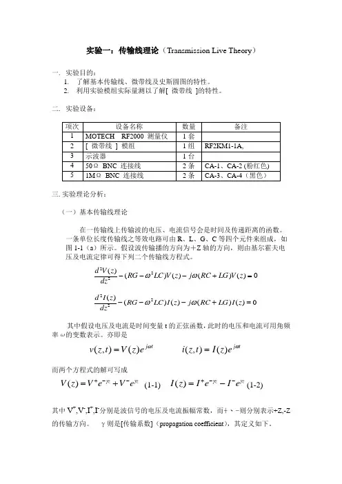
实验一:传输线理论(Transmission Live Theory )一. 实验目的:1. 了解基本传输线、微带线及史斯圆图的特性。
2. 利用实验模组实际量测以了解[ 微带线 ]的特性。
二. 实验设备:三. 实验理论分析:(一)基本传输线理论在一传输线上传输波的电压、电流信号会是时间及传递距离的函数。
一条单位长度传输线之等效电路可由R 、L 、G 、C 等四个元件来组成,如 图1-1(a )所示。
假设波传输播的方向为+Z 轴的方向,则由基尔霍夫电 压及电流定律可得下列二个传输线方程式。
其中假设电压及电流是时间变量t 的正弦函数,此时的电压和电流可用角频率ω的变数表示。
亦即是而两个方程式的解可写成z ze V eV z V γγ--++=)( (1-1) zze I eI z I γγ--+-=)((1-2)其中V +,V -,I +,I -分别是波信号的电压及电流振幅常数,而+、-则分别表示+Z,-Z 的传输方向。
γ则是[传输系数](propagation coefficient ),其定义如下。
)()()()()(222=+---z V LG RC j z V LC RG dzz V d ωω0)()()()()(222=+---z I LG RC j z I LC RG dzz I d ωωtj ez V t z v ω)(),(=tj ez I t z i ω)(),(=0 ))((C j G L j R ωωγ++=(1-3)))((C j G L j R ωωγ++=而波在z 上任一点的总电压及电流的关系则可由下列方程式表示。
I L j R dzdV ⋅+-=)(ωV C j G d zd I ⋅+-=)(ω (1-4)将式(1-1)及(1-2)代入式(1-3)可得Cj G IVωγ+=++一般将上式定义为传输线的[特性阻抗](Characteristic Impedance ),Z O 。
目录第一章射频传输理论简介 (4)1.1.1 带宽 (4)1.2 射频线的结构和功能 (5)1.2.1射频传输线的种类 (5)1.2.2典型的射频线 (6)1.2.3射频线的电磁场 (6)1.2.4射频传输线中的电阻和电抗 (7)1.2.5当介质为空气时,能量波的传播速度为光速C: (8)1.2.6截止频率 (9)1.2.7波长和频率 (10)1.2.8传输速率 (10)1.3 反射 (11)1.3.1反射波 (12)1.3.2不同中断的反射 (12)1.3.3失配的定义 (13)1.3.4 RL,VSWR,Γ之间关系 (15)1.3.5两次以上的中断产生的确反射 (16)1.4 RF线的损耗、(射频传输线=RF线) (17)1.4.1损耗=10log(Power out)/(Power in) |dB| (17)1.4.2内、外导体、介质材料对损耗的影响。
(17)1.4.3护套 (18)1.5 趋肤效应 (19)1.6 无源互调(PIMI) (20)1.6.1说明 (21)第二章材料 (22)2.1 接触材料和表面处理 (22)2.1.1要求与设计 (22)2.2 基础材料 (26)2.2.1 紫铜 (26)2.2.2铍青铜 (26)2.2.3锡磷青铜 (27)2.2.4黄铜 (27)2.2.5不锈钢 (27)2.2.6铝合金 (27)2.3 镀层材料 (28)2.3.1 金 (28)2.3.2 银 (29)2.3.3 镍 (30)2.3.4 锡铅合金 (30)2.3.5 三元合金(铜—锡—锌合金) (30)12.4 塑料和橡胶 (31)2.4.1 PE(聚乙烯) (31)2.4.2 PTFE(聚四氟乙烯) (31)2.4.3 PFA (31)2.4.4 PEEK (Polyether-Etherketone) (32)2.4.5 PPO (32)2.4.6硅树脂橡胶 (32)第三章射频连接器设计 (33)3.1 功能和性能 (33)3.1.1电气性能 (33)3.2.2机械性能 (34)3.1.3环境性能 (35)3.2 同轴连接器设计 (35)3.2.1连接的种类 (35)3.2.2同轴连接器的组成 (36)3.2.3接触力 (40)3.3 连接机构 (43)3.3.1螺纹连接机构 (44)3.2.2卡口式连接机构 (44)3.3.3推入式连接 (44)3.3.4滑入式连接机构 (45)3.3.5推入自锁式连接 (45)3.4 固定 (45)3.4.1电缆内导体的固定 (46)3.4.2与电缆外导体的固定 (46)3.4.3面板固定 (48)3.3.4固定到印制板上 (49)3.4.5安装工具和指南 (49)3.5 同轴连接器的系列及电缆 (50)3.5.1同轴连接器的系列 (50)3.5.2同轴电缆 (50)3.5.3电缆的电气性能 (54)3.5.4电缆的类型和特征 (55)3.5.5微型连接器 (55)3.5.6超小型连接器 (56)3.5.7微型连接器 (59)3.5.8中等连接器 (60)3.5.9大型连接器 (62)3.5.10精度连接器 (62)3.5.11一体式和连接式适配器 (63)3.6 标准 (64)第四章测试和测量 (65)4.1 测量理论和方法..............................................................................错误!未定义书签。