TIL191中文资料
- 格式:pdf
- 大小:86.39 KB
- 文档页数:6
TIL191, TIL192, TIL193, TIL191A, TIL192A, TIL193A
TIL191B, TIL192B, TIL193B
OPTOCOUPLERS
SOES026B – APRIL 1989 – REVISED APRIL 1998
1
POST OFFICE BOX 655303 •
DALLAS, TEXAS 75265D
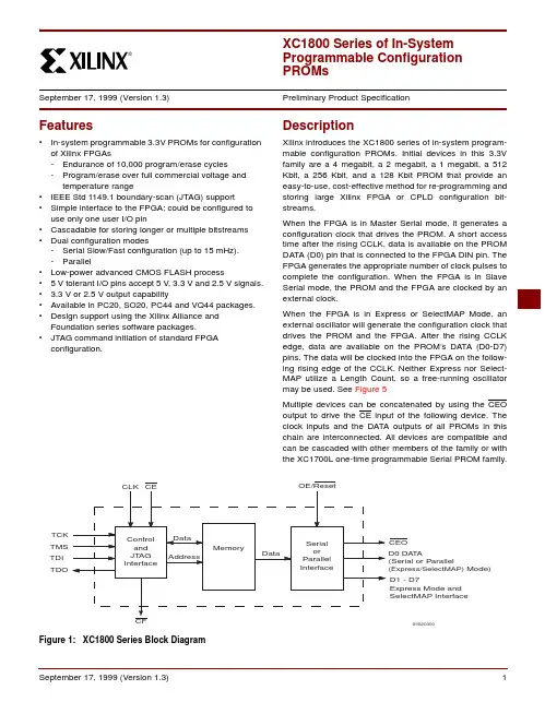
Gallium-Arsenide-Diode Infrared Source
D
Source Is Optically Coupled to Silicon npn
Phototransistor
D
Choice of One, Two, or Four Channels
D
Choice of Three Current-Transfer RatiosD
High-Voltage Electrical Isolation 3.535 kV
Peak (2.5 kV rms)
D
Plastic Dual-In-Line Packages
D
UL Listed — File #E65085
description
These optocouplers consist of one gallium-arsenide light-emitting diode and one silicon npn phototransistor per
channel. The TIL191 has a single channel in a 4-pin package, the TIL192 has two channels in an 8-package,
and the TIL193 has four channels in a 16-pin package. The standard devices, TIL191, TIL192, and TIL193, are
tested for a current-transfer ratio of 20% minimum. Devices selected for a current-transfer ratio of 50% and
100% minimum are designated with the suffix A and B respectively.
schematic diagrams
TIL192
1
2
3
48
7
6
51ANODE
1CATHODE
2ANODE
2CATHODE1COLLECTOR
1EMITTER
2COLLECTOR
2EMITTERTIL191
1
24
3ANODE
CATHODECOLLECTOR
EMITTERTIL193
1
2
3
416
15
14
131ANODE
1CATHODE
2ANODE
2CATHODE1COLLECTOR
1EMITTER
2COLLECTOR
2EMITTER
5
6
7
812
11
10
93ANODE
3CATHODE
4ANODE
4CATHODE3COLLECTOR
3EMITTER
3COLLECTOR
3EMITTER
absolute maximum ratings at 25°C free-air (unless otherwise noted)†
Input-to-output voltage (see Note 1) ±3.535 kV peak or dc (±2.5 kV rms). . . . . . . . . . . . . . . . . . . . . . . . . . . . . .
Collector-emitter voltage (see Note 2) 35 V. . . . . . . . . . . . . . . . . . . . . . . . . . . . . . . . . . . . . . . . . . . . . . . . . . . . . . . .
Emitter-collector voltage 7 V. . . . . . . . . . . . . . . . . . . . . . . . . . . . . . . . . . . . . . . . . . . . . . . . . . . . . . . . . . . . . . . . . . . . .
Input diode reverse voltage 5 V. . . . . . . . . . . . . . . . . . . . . . . . . . . . . . . . . . . . . . . . . . . . . . . . . . . . . . . . . . . . . . . . . .
Input diode continuous forward current at (or below) 25°C free-air temperature (see Note 3) 50 mA. . . . . . .
Continuous total power dissipation at (or below) 25°C free-air temperature:
Phototransistor (see Note 4) 150 mW. . . . . . . . . . . . . . . . . . . . . . . . . . . . . . . . . . . . . . . . . . . . . . . . . . . . . . . . . .
Input diode plus phototransistor per channel (see Note 5) 200 mW. . . . . . . . . . . . . . . . . . . . . . . . . . . . . . . .
Storage temperature range, T
stg –55°C to 125°C. . . . . . . . . . . . . . . . . . . . . . . . . . . . . . . . . . . . . . . . . . . . . . . . . . .
Lead temperature 1,6 mm (1/16 inch) from case for 10 seconds 260°C. . . . . . . . . . . . . . . . . . . . . . . . . . . . . . .
†
Stresses beyond those listed under “absolute maximum ratings” may cause permanent damage to the device. These are stress ratings only, and
functional operation of the device at these or any other conditions beyond those indicated under “recommended operating conditions” is not
implied. Exposure to absolute-maximum-rated conditions for extended periods may affect device reliability.
NOTES:1.This rating applies for sine-wave operation at 50 Hz or 60 Hz. This capability is verified by testing in accordance with UL requirements.
2.This value applies when the base-emitter diode is open circuited.
3.Derate linearly to 100°C free-air temperature at the rate of 0.67 mA/°C.
4.Derate linearly to 100°C free-air temperature at the rate of 2 mW/°C.
5.Derate linearly to 100°C free-air temperature at the rate of 2.67 mW/°C.
Copyright © 1998, Texas Instruments Incorporated
PRODUCTION DATA information is current as of publication date.
Products conform to specifications per the terms of Texas Instruments
standard warranty. Production processing does not necessarily include
testing of all parameters.元器件交易网www.cecb2b.comTIL191, TIL192, TIL193, TIL191A, TIL192A, TIL193A
TIL191B, TIL192B, TIL193B
OPTOCOUPLERS
SOES026B – APRIL 1989 – REVISED APRIL 1998
2
POST OFFICE BOX 655303 •
DALLAS, TEXAS 75265electrical characteristics 25°C free-air temperature range (unless otherwise noted)
PARAMETERTEST CONDITIONSMINTYPMAXUNIT
V
(BR)CEOCollector-emitter breakdown voltageI
C = 0.5 mA,I
F = 035V
V
(BR)ECOEmitter-collector breakdown voltageI
C = 100 µA,I
F = 07V
I
RInput diode static reverse currentV
R = 5 V10µA
I
C(off))Off-state collector currentV
CE = 24 V,I
F = 0100nA
TIL191, TIL192, TIL19320%
CTRCurrent transfer ratioTIL191A, TIL192A, TIL193AI
F = 5 mA,V
CE = 5 V50%
TIL191B, TIL192B, TIL193B100%
V
FInput diode static forward voltageI
F = 20 mA1.4V
V
CE(sat)Collector-emitter saturation voltageI
F = 5 mA,I
C = 1 mA0.4V
C
ioInput-to-output capacitanceV
in–out = 0 mA,