
PMD1602K中文资料
- 格式:pdf
- 大小:54.03 KB
- 文档页数:1

Contents1. Precautions in Use of LCD Module-----------------------------------P32. General Specification-------------------------------------------------------P33. Absolute Maximum Ratings----------------------------------------------P34. Electrical Characteristics--------------------------------------------------P45. Backlight Information-------------------------------------------------------P46. Optical Characteristics-----------------------------------------------------P57. Interface Description--------------------------------------------------------P68. Contour Drawing & Block Diagram--------------------------------------P79. Application circuit----------------------------------------------------------P810. LCM Function Description-----------------------------------------------P811. User instruction Definitions--------------------------------------------P10 11.1 Instruction table----------------------------------------------------P1011.2 Instruction description --------------------------------------------P1112. Timing Characteristics -------------------------------------------------P1413. Initializing flow chart ----------------------------------------------------P1514. Standard Character pattern--------------------------------------------P1715.Revision records------------------------------------------------------P181. Precautions in Use of LCD Module(1) Avoid applying excessive shocks to the module or making any alterations or modifications to it.(2) Don’t make extra holes on the printed circuit board, modify its shape or change the components of LCDModule.(3) Don’t disassemble the LCM.(4) Don’t operate it above the absolute maximum rating.(5) Don’t drop, bend or twist LCM.(6) Soldering: only to the I/O terminals.⑺ Storage: please storage in anti-static electricity container and clean environment.2. General SpecificationITEM STANDARD VALUE UNIT Number of dots 16X2 CHARs DotsOutline dimension 80.0(W)X36.0(H)X12.8MAX.(T) mm View area 65.0(W)X16.0(H) mmActive area 56.21(W)X11.50(H) mmDot size 0.56(W)X0.66(H) mmDot pitch 0.60(W)X0.70(H) mmLCD type STN,Blue,Negative,TransmissiveView direction 6 o’clockBacklight White LEDController SPLC780D1-0013. Absolute Maximum RatingsITEM SYMBOL MIN. TYP. MAX. UNIT Operating Temperature T OP-20 -+70 ℃Storage Temperature T ST-30 -+80 ℃Input Voltage V I0 -V DD V Supply Voltage For Logic V DD0 - 5.5 V Supply Voltage For LCD V DD-V EE0 - 5 V4. Electrical CharacteristicsITEM SYMBOL CONDITION MIN. TYP. MAX. UNIT Logic Voltage V DD-V SS- 4.5 5.0 5.5 V Supply Voltage For LCD V DD-V O Ta=25℃--- 4.5 --- V Input High Volt. V IH- 2.0 -V DD V Input Low Volt. V IL--0.3 -0.8 V Output High Volt. V OH I oH=-0.2mA 2.4 -V DD V Output Low Volt. V OL I oL=1.6mA0 -0.4 V Supply Current I DD---- 1.0 --- mA 5. Backlight InformationAbsolute Maximum ratings (Ta=25℃)Item Symbol Conditions Rating Unit Reverse voltage Vr - 5.0 V Reverse Current I r Vr=5.0V 80 uA Absolute maximum forward Current Ifm 100 mA Peak forward current Ifp I msec plus 10% Duty Cycle 240 mA Power dissipation P d340 mW Operating Temperature Range T oper-30~+70 ℃Storage Temperature Range Tst -40~+80 ℃Electrical/Optical Characteristics (Ta=250C,If=20mA)Color Wavelengthλp(nm)Spectral line halfwidthΔλ(nm)Operating Voltage(V)(±0.15V)ForwardCurrent (mA)White--- --- 3.1 206. Optical CharacteristicsITEM SYMBOL CONDITION MIN TYP MAX UNIT View Angle(V)θCR≧2 10 -120 deg.(H)φCR≧2 -45 -45 deg.Contrast Ratio CR -- 5 --ResponseT rise --200 300 ms Time T fall --150 200 ms7.Interface DescriptionPin No. Symbol Level Description1 V SS0V Ground2 V DD 5.0V Power supply for Logic3 V O(Variable) Supply voltage for LCD Panel4 RS H/L H:Data L :Instruction5 RW H/L H:Read L:Write6 E H/L Enable signal7~14 DB0~DB7 H/L Data bus. DB7 is used for Busy Flag .15 A(LED+) +5V Anode of LED Backlight16 K(LED-) 0V Cathode of LED Backlight8. Contour Drawing & Block Diagram9. Application circuit10. LCM Function DescriptionThe LCD display Module is built in a LSI controller, the controller has two 8-bit registers, an instruction register (IR) and a data register (DR).The IR stores instruction codes, such as display clear and cursor shift, and address information for display data RAM (DDRAM) and character generator (CGRAM). The IR can only be written from the MPU. The DR temporarily stores data to be written or read from DDRAM or CGRAM. When address information is written into the IR, then data is stored into the DR from DDRAM or CGRAM. By the register selector (RS) signal, these two registers can be selected.Various Kinds of Operations according to RS and R/W BitsRS R/W Operation0 0 IR write as an internal operation (display clear, etc.)0 1 Read busy flag (DB7) and address counter (DB0 to DB7)1 0 Write data to DDRAM or CGRAM (DR to DDRAM or CGRAM)1 1 Read data from DDRAM or CGRAM (DDRAM or CGRAM to DR)Busy Flag (BF)When the BF= "High", it indicates that the LCM internal operation is being processed. So during this time the next instruction cannot be accepted. BF can be read, when RS = Low and R/W = High (Read Instruction Operation), through DB7 port. Before executing the next instruction, be sure that BF is not High.Address Counter (AC)Address Counter(AC) stores DDRAM/CGRAM address. After writing into (reading from) DDRAM/CGRAM, AC is automatically increased (decreased) by 1. When RS = "Low" and R/W = "High", AC can be read through DB0 - DB6 ports.Display Data RAM (DDRAM)This DDRAM is used to store the display data represented in 8-bit character codes. Below figure is the relationships between DDRAM addresses and positions on the liquid crystal display.LCM DDRAM Address(In HEX)Character Generator ROM (CGROM)The CGROM generate 5×8 dot or 5×10 dot character patterns from 8-bit character codes. See “Standard Character pattern”. Character Generator RAM (CGRAM)In CGRAM, the user can rewrite character by program. Relationship between Character Code (DDRAM) and Character Pattern (CGRAM) shown below.“X”: don’t care16 CHARs X 2 Lines DisplayNo.12345678910 11 12 13 14 15 161st Line 00 01 02 03 04 05 06 07 08 09 0A 0B 0C 0D 0E 0F 2nd Line 40 41 42 43 44 45 46 47 48 49 4A 4B 4C 4D 4E 4FChar Code(DDRAM data) CGRAM address CGRAM dataD7 D6 D5 D4 D3 D2 D1 D0 A5 A4 A3 A2 A1 A0 P7 P6 P5 P4 P3 P2 P1 P0 Patternnumber0 0 0 0 X 0 0 0 0 0 0 0 0 0 X X X 0 1 1 1 00 0 1 1 0 0 0 1 0 1 0 1 0 0 0 1 0 1 1 1 1 1 1 1 1 0 0 1 0 0 0 1 1 0 1 1 0 0 0 1 1 1 0 1 0 0 0 1 . . . . . . . . ... . . . 1 1 1 . . . . . . . 0 0 0 0 0 Pattern 1. . . . . . . . . . . .. . .0 0 0 0 X 1 1 1 1 1 1 0 0 0 X X X 1 0 0 0 10 0 1 1 0 0 0 1 0 1 0 1 0 0 0 1 0 1 1 1 1 1 1 1 1 0 0 1 0 0 0 1 1 0 1 1 0 0 0 1 1 1 0 1 0 0 0 1 . . . . . . . . . . . . . . 1 1 1 . . .. . . . 0 0 0 0 0Pattern 8Example: DDRAM addresses 4E AC (Hexadecimal)AC6 AC5 AC4 AC3 AC2 AC1 AC0111111. User instruction Definitions 11.1 Instruction tableInstruction CodeInstructionRS R/W DB7 DB6 DB5 DB4 DB3 DB2 DB1 DB0 DescriptionExecutiontimef OSC=270KHz)Clear Display 0 0 0 0 0 0 0 0 0 1Write “20H”to DDRAMand set DDRAM addressto “00H”from AC.1.52msReturn Home 0 0 0 0 0 0 0 0 1 XSet DDRAM address to“00H”from AC and returncursor to its originalposition if shifted. Thecontents of DDRAM arenot changed.1.52msEntry Mode Set 0 0 0 0 0 0 0 1 I/D SHAssign cursor movingdirection and make shift ofentire display enable.37sDisplayON/OFF control 0 0 0 0 0 0 1 D C BSet display(D), cursor(C),and blinking of cursor(B)on/off control bit.37sCursor or Display Shift 0 0 0 0 0 1 S/C R/L X XSet cursor moving anddisplay shift control bit,and the direction, withoutchanging DDRAM data.37sFunction Set 0 0 0 0 1 DL N F X X Set interface datalength(DL:4-bit/8-bit),numbers of display line(N:1-line/2-line), display fonttype(F: 5X8 dots/ 5X11dots)37sSet CGRAM Address 0 0 0 1 AC5 AC4 AC3 AC2 AC1 AC0Set CGRAM address inaddress counter.37sSet DDRAM Address 0 0 1 AC6 AC5 AC4 AC3 AC2 AC1 AC0Set DDRAM address inaddress counter.37sRead BusyFlag and Address 0 1 BF AC6 AC5 AC4 AC3 AC2 AC1 AC0Whether during internaloperation or can not beknown by reading BF. Thecontents of addresscounter can also be read.0sWrite Data to RAM 1 0 D7 D6 D5 D4 D3 D2 D1 D0Write data into internalRAM DDRAM/CGRAM).43sRead Data from RAM 1 1 D7 D6 D5 D4 D3 D2 D1 D0Read data from internalRAM (DDRAM/CGRAM).43sRemark:‘X’don’t care11.2 Instruction Description1)Clear DisplayRS RW DB7 DB6 DB5 DB4 DB3 DB2 DB1 DB00 0 0 0 0 0 0 0 0 1Clear all the display data by writing "20H" (space code) to all DDRAM address, and set DDRAM address to "00H" into AC (address counter). Return cursor to the original status. Namely, bring the cursor to the left edge on first line of the display. Make entry mode increment (I/D = "1").2) Return HomeRS RW DB7 DB6 DB5 DB4 DB3 DB2 DB1 DB00 0 0 0 0 0 0 0 1 -Return Home is cursor return home instruction. Set DDRAM address to "00H" into the address counter. Return cursor to its original site and return display to its original status, if shifted. Contents of DDRAM do not change.3) Entry Mode SetRS RW DB7 DB6 DB5 DB4 DB3 DB2 DB1 DB00 0 0 0 0 0 0 1 I/D SHSet the moving direction of cursor and display.I/D: Increment / decrement of DDRAM address (cursor or blink)When I/D = "High", cursor/blink moves to right and DDRAM address is increased by 1. When I/D = "Low", cursor/blink moves to left and DDRAM address is decreased by 1.* CGRAM operates the same as DDRAM, when read from or write to CGRAM.SH: Shift of entire displayWhen DDRAM read (CGRAM read / write) operation or SH = "Low", shift of entire display is not performed. If SH = "High" and DDRAM write operation, shift of entire display is performed according to I/D value:I/D ="1" : shift left,I/D = "0" : shift right.4) Display ON/OFF ControlRS RW DB7 DB6 DB5 DB4 DB3 DB2 DB1 DB00 0 0 0 0 0 1 D C BControl display / cursor / blink ON / OFF 1 bit register.D: Display ON / OFF control bitWhen D = "High", entire display is turned on.When D = "Low", display is turned off, but display data is remained in DDRAM.C: Cursor ON / OFF control bitWhen C = "High", cursor is turned on.When C = "Low", Cursor is disappeared in current display, but I/D register remains its data. B: Cursor Blink ON / OFF control bitWhen B = "High", cursor blink is on, that performs alternate between all the high data and display character at the cursor position.When B = "Low", blink is off.5) Cursor or Display ShiftRS RW DB7 DB6 DB5 DB4 DB3 DB2 DB1 DB00 0 0 0 0 1 S/C R/L - -Shifting of right/left cursor position or display Without Writing or reading of display data, shift right/left cursor position or display. This instruction is used to correct or search display data. (refer to Table 4) During 2-line mode display, cursor moves to the 2nd line after 40th digit of 1st line. Note that display shift is performed simultaneously in all the line. When displayed data is shifted repeatedly, each line shifted individually. When display shift is performed, the contents of address counter are not changed.S/C R/L Operation0 0 Shift the cursor to the left, AC is decreased by 1.0 1 Shift the cursor to the right, AC is increased by 1.1 0 Shift all the display to the left, cursor moves according to the display.1 1 Shift all the display to the right, cursor moves according to the display.6) Function SetRS RW DB7 DB6 DB5 DB4 DB3 DB2 DB1 DB00 0 0 0 1 DL N F - -DL: Interface data length control bitWhen DL = "High", it means 8-bit bus mode with MPU.When DL = "Low", it means 4-bit bus mode with MPU.When 4-bit bus mode, it needs to transfer 4-bit data by two times.N: Display line number control bitWhen N = "Low", it means 1-line display mode.When N = "High", 2-line display mode is set.F: Display font type control bitWhen F = "Low", it means 5 x 8 dots format display modeWhen F = "High", 5 x11 dots format display mode.7) Set CGRAM AddressRS RW DB7 DB6 DB5 DB4 DB3 DB2 DB1 DB00 0 0 1 AC5 AC4 AC3 AC2 AC1 AC0Set CGRAM address to AC. This instruction makes CGRAM data available from MPU.8) Set DDRAM AddressRS RW DB7 DB6 DB5 DB4 DB3 DB2 DB1 DB00 0 1 AC6 AC5 AC4 AC3 AC2 AC1 AC0Set DDRAM address to AC.This instruction makes DDRAM data available from MPU. When 1-line display mode (N = 0), DDRAM address is from "00H" to "4FH". In 2-line display mode (N = 1), DDRAM address is the 1st line is from "00H" to "27H", and DDRAM address in the 2nd line is from "40H" to "67H".9) Read Busy Flag & AddressRS RW DB7 DB6 DB5 DB4 DB3 DB2 DB1 DB00 1 BF AC6 AC5 AC4 AC3 AC2 AC1 AC0This instruction shows whether LCM is in internal operation or not. If the resultant BF is High, it means the internal operation is in progress and you have to wait until BF to be Low, and then the next instruction can be performed. In this instruction you can read also the value of address counter.10) Write data to RAMRS RW DB7 DB6 DB5 DB4 DB3 DB2 DB1 DB01 0 D7 D6 D5 D4 D3 D2 D1 D0Write binary 8-bit data to DDRAM/CGRAM.The selection of RAM from DDRAM, CGRAM, is set by the previous address set instruction: DDRAM address set, CGRAM address set. RAM set instruction can also determine the AC direction to RAM. After write operation, the address is automatically increased/decreased by 1, according to the entry mode.11) Read data from RAMRS RW DB7 DB6 DB5 DB4 DB3 DB2 DB1 DB01 1 D7 D6 D5 D4 D3 D2 D1 D0Read binary 8-bit data from DDRAM/CGRAM.The selection of RAM is set by the previous address set instruction. If address set instruction of RAM is not performed before this instruction, the data that read first is invalid, because the direction of AC is not determined. If you read RAM data several times without RAM address set instruction before read operation, you can get correct RAM data from the second, but the first data would be incorrect, because there is no time margin to transfer RAM data.In case of DDRAM read operation, cursor shift instruction plays the same role as DDRAM addressset instruction : it also transfer RAM data to output data register. After read operation address counter is automatically increased/decreased by 1 according to the entry mode. After CGRAM read operation, display shift may not be executed correctly.* In case of RAM write operation, after this AC is increased/decreased by 1 like read operation. In this time, AC indicates the next address position, but you can read only the previous data by read instruction.12. Timing Characteristics13.Initializing flow chart l 8-bit interface model 4-bit interface mode14. Standard Character pattern15. Revision recordsVersion Ref.pages Revision Items DateA00All pages New release 2012.02.28。
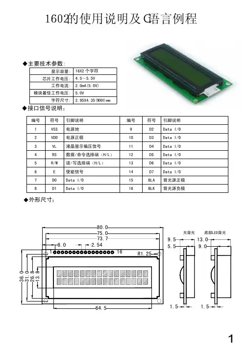

1602液晶资料一、介绍1602液晶是一种常见的字符型液晶显示器,可以显示16列2行共32个字符。
它采用了液晶显示技术,使得显示效果更加清晰、稳定。
1602液晶广泛应用于各种嵌入式系统、电子设备以及 DIY 项目中。
本文将介绍1602液晶的基本原理、接口定义、使用方法以及常见应用场景。
二、基本原理1602液晶的基本原理是利用液晶分子的取向和电场作用的变化来改变光的透过与反射。
它由1602个独立的像素(80列×2行)组成,每个像素有一个电极对和一个液晶分子,液晶分子的取向可以通过施加电场来改变。
1602液晶由背光源、液晶面板、驱动电路和控制电路等组成,背光源提供背光使得字符能够显示在显示器上。
三、接口定义1602液晶显示器通常通过并行接口与主控单元进行通信,下面是1602液晶的常用接口定义:•DB0-DB7:并行数据接口,用于传输数据与指令。
•RS:指令/数据选择信号,用于控制将数据写入显示器还是发送给控制器.•R/W:读/写选择信号,用于选择进行读操作或写操作。
•E:使能信号,用于控制读写操作的时序。
•VSS:地线,用于提供电流的回路。
•VDD:电源正极,提供1602液晶的工作电源。
•V0:液晶偏置电压,通过该电压设置液晶显示的对比度。
•A:背光灯电源正极,提供背光灯的工作电源。
•K:背光灯电源负极,提供背光灯工作电流的回路。
四、使用方法使用1602液晶显示器需要以下步骤:1.连接电路:根据接口定义,将1602液晶与主控单元进行正确的连接。
注意接线的准确性,以免引起电路故障。
2.初始化:在使用1602液晶之前,需要对其进行初始化。
初始化的过程一般包括设置显示模式、清屏以及设置光标位置等。
3.写入数据:通过并行接口将想要显示的数据或指令传输给1602液晶,可以显示各种字符、数字、符号等。
4.控制显示:通过指令设置1602液晶的显示方式,包括光标显示、光标闪烁、显示开关等。
5.清屏:清除1602液晶的显示内容,可以使用指令或者写入空格字符来实现。
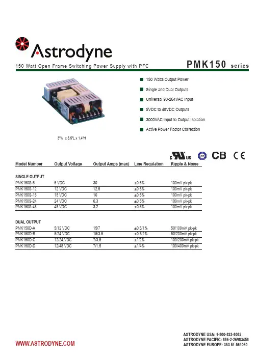
150 Watts Output Power Single and Dual Outputs Universal 90-264VAC Input 5VDC to 48VDC Outputs 3000VAC Input to Output Isolation Active Power Factor Correctionmodel NumberOutput Voltage Output Amps (max) Line Regulation Ripple & NoiseSINGLE OUTPUT PMK150S-5 5 VDC 30 ±0.5% 100mV pk-pk PMK150S-12 12 VDC 12.5 ±0.5% 100mV pk-pk PMK150S-15 15 VDC 10 ±0.5% 100mV pk-pk PMK150S-24 24 VDC 6.3 ±0.5% 100mV pk-pk PMK150S-48 48 VDC 3.2 ±0.5% 100mV pk-pkDUAL OUTPUT PMK150D-A 5/12 VDC 15/7 ±0.5/1% 50/100mV pk-pk PMK150D-B 5/24 VDC 15/3.5 ±0.5/2% 50/200mV pk-pk PMK150D-C 12/24 VDC 7/3.5 ±1/2% 100/200mV pk-pk PMK150D-D12/48 VDC 7/1.5 ±1/4% 100/400mV pk-pk3”W x 5.5”L x 1.4”HINPUT SPECIFICATIONSInput Voltage Range 90-264 VACFrequency Range47-63 Hz Power Factor Correction 0.96 to 0.98 Inrush Current, typ: 30A @ 115VAC60A @ 230VAC *OUTPUT SPECIFICATIONSVoltage and Current (Note 6) See Selection ChartLine Regulation (Note 8) See Selection Chart Load Regulation (10%-FL, Note 7) Singles: ± 0.5%, typ Duals: ±3/5%, typ Preset Accuracy (Note 9) ±1%, typ DC Voltage Adjust (typ) ±6%, typ Temperature Coefficient ±0.05%/°C Ripple/Noise (Notes 1, 3, 10) See Selection Chart Over Voltage Protection Latching, Auto Recover after fault condition is removed * Short Circuit Protection Latching, Auto Recover after fault condition is removed * Hold Up Time 20mS, typ (Nom I/P, FL)GENERAL SPECIFICATIONSIsolation (Note 4) I/P-O/P: 3000VAC I/P-Ground: 2000VAC O/P-Ground: 500 VAC Efficiency75%, min.Switching Frequency 67Khz, (fixed, typical) SafetyUL,TUV, CB, CEENVIRONmENTAL SPECIFICATIONSOper. Temperature -10 to +70°C(See Derate Curve) Storage Temperature -25 to +85°C *Relative Humidity 0% to +95%, non-cond * EMC EN55011 Class B MTBF 270,000 HrsMil Std 217, 25°CPHYSICAL SPECIFICATIONSSize3” x 5.5” x 1.4” Construction Open Frame Weight0.5 lb, (226g)NOTES* These are stress ratings. Exposure of the devices to any of these conditionsmay adversely affect long term reliability. Proper operation under conditions other than the standard operating conditions is neither warranteed nor implied.All specifications are typical at nominal input, full load, and 25°C unless other-wise notedAstrodyne products are not authorized or warranteed for use as critical components in life support systems, equipment used in hazardous environments, nuclear controls systems, or other mission-critical applications.1. All measurements should be made directly at the terminals of the power supply2. All specifications typical @ 25°C, unless otherwise noted, at nominal line and load.3. Ripple and noise dependent upon output voltage as specified per particular model.4. Isolation for up to 1 minute duration.5. Specified for free air convection cooling.6. Minimum load is not required for proper operation.7. Load Regulation is measured by change ±40% of measured output load from 60% full load, with the other output set to 60% full load.8. Line Regulation measured from 90-264VAC. 100VAC minimum required for full load start.9. Preset Accuracy measured at nominal load, 120VAC input.10. O/P Noise measured directly at the pins/terminals at nominal load, 0.1uF bypass and 47uF electrolytic, pk-pk @ 20MHz bandwidth.2.00±0.50mm0.079±0.020in[]5.70mm[0.224in]134.00mm[5.276in]139.70mm [5.500in]5.mm[.197in]71.2mm[2.83in]76.2mm[3.in]4_Ø3.40mm[0.134in]35.00 mm [1.378 in]1 2 39 8 7 6 5 4mECHANICAL DImENSIONSPin # Outputs1 GND2 ACN3 ACL4 + Output5 + Output6 Common7 Common8 CommonOUTPUT DERATING CURVE - SINGLE OUTPUT OUTPUT DERATING CURVE - DUAL OUTPUT1. Forced air colling 10 CFM2. Free air convection- Open Frame, U-Channel3. Free air convection- Enclosed。