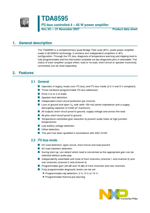
1.General descriptionThe TDA8595 is a complementary quad Bridge Tied Load (BTL) audio power amplifier made in BCDMOS technology. It contains four independent amplifiers in BTLconfiguration.Through the I 2C-bus,diagnosis of temperature warning and clipping level is fully programmable and the information available via two diagnostic pins is selectable.The status of each amplifier (output offset, load or no load, short-circuit or speaker incorrectly connected) can be read separately.2.Features2.1GeneralI Operates in legacy mode (non I 2C-bus) and I 2C-bus mode (3.3 V and 5 V compliant)I Three hardware-programmable I 2C-bus addresses I Drive 4Ω or 2Ω loads I Speaker fault detectionI Independent short-circuit protection per channelI Loss of ground and open V P safe (with 150m Ω series impedance and a supply decoupling capacitor of 2200µF maximum)I All outputs short-circuit proof to ground, supply voltage and across the load I All pins short-circuit proof to groundI Temperature-controlled gain reduction to prevent audio holes at high junction temperaturesI Low battery voltage detection I Offset detectionIThis part has been qualified in accordance with AEC-Q1002.2I 2C-bus modeI DC load detection: open-circuit, short-circuit and load present I AC load (tweeter) detectionI During start-up, can detect which load is connected so the appropriate gain can be selected without audio popI Independently selectable soft mute of front channels (channel 1 and channel 3) and rear channels (channel 2 and channel 4)I Programmable gain (26 dB and 16 dB) of front channels and rear channels I Fully programmable diagnostic levels can be set:N Programmable clip detection: 2%, 5% or 10%N Programmable thermal pre-warningTDA8595I 2C-bus controlled 4×45 W power amplifierRev. 02 — 21 November 2007Product data sheetI Selectable information on the DIAG and STB pins:N The STB pin can be programmed/multiplexed with second clip detectionN Clip information of each channel can be directed separately to the DIAG pin or the STB pinN Independent enabling of thermal, clip or load fault detection (short across or to V Por to ground) on DIAG pin3.Quick reference data4.Ordering informationTable 1.Quick reference dataRefer to test circuit (see Figure 30) at V P =V P1=V P2=14.4V; R L =4Ω; f =1kHz; R S =0Ω;normal mode; unless otherwise specified. Tested at T amb =25°C; guaranteed for T amb =−40°C to +105°C.Symbol Parameter Conditions Min Typ Max Unit V P supply voltage R L =4Ω814.418V I q quiescent current no load -270400mAP ooutput powerV P =14.4VR L =4Ω; THD =0.5%1820-W R L =4Ω; THD =10%2325-W R L =4Ω; maximum power; V i =2V (RMS)square wave3740-WR L =2Ω; maximum power; V i =2V (RMS)square wave5864-WTHD total harmonic distortion R L =4Ω; f =1kHz;P o =1W to 12W -0.010.1%V n(o)noise output voltagefilter 20Hz to 22kHz;R S =1k Ωnormal mode -4565µV line driver mode-2229µVTable 2.Ordering informationType number Package Name DescriptionVersion TDA8595J DBS27P plastic DIL-bent-SIL (special bent) power package;27leads (lead length 6.8 mm)SOT827-1TDA8595TH HSOP36plastic, heatsink small outline package; 36 leads;low stand-off heightSOT851-2TDA8595SDRDBS27Pplastic rectangular-DIL-bent-SIL (reverse bent) power package; 27leads (row spacing 2.54 mm)SOT878-15.Block diagramThe pin numbers in parenthesis represent TDA8595TH.Fig 1.Block diagram001aad135STANDBY/FAST MUTEI 2C-BUS INTERFACECLIP DETECT/DIAGNOSTICMUTEPROTECTION/DIAGNOSTIC26 dB/16 dBPROTECTION/DIAGNOSTIC26 dB/16 dBPROTECTION/DIAGNOSTIC26 dB/16 dBPROTECTION/DIAGNOSTIC26 dB/16 dBMUTEMUTEMUTE5 (33)10 (4)8 (2)18 (14)20 (17)6 (30)4 (32)22 (25)24 (23)27 (36)17 (13)9 (3)14 (9)SGNDSVRADSEL SDAV P1V P2IN4IN2IN3IN1STBACGNDPGND1PGND3PGND411 (5)15 (11)13 (7)16 (12)12 (6)1 (28)26 (26)SCL23 (22)21 (20, 21)7 (34, 35)2 (29)3 (31)19 (16)25 (24)DIAGOUT1+OUT1−OUT3+OUT3−OUT2+OUT2−OUT4+OUT4−TABV PPGND2TDA8595J TDA8595SD (TDA8595TH)6.Pinning information6.1PinningFig 2.Pin configuration TDA8595J and TDA8595SDTDA8595J TDA8595SD001aad136ADSEL STB PGND2OUT2−DIAG OUT2+V P2OUT1−PGND1OUT1+SVR IN1IN2SGND IN4IN3ACGND OUT3+PGND3OUT3−V P1OUT4+SCL OUT4−PGND4SDA TAB 1234567891011121314151617181920212223242526276.2Pin descriptionFig 3.Pin configuration TDA8595THTDA8595THDIAG n.c.OUT2−OUT1−PGND2PGND1OUT2+TAB V P2V P2OUT1+STB SVR ADSEL IN1n.c.IN2SDA n.c.OUT4+SGNDn.c.IN4IN3001aad138363534333231302928272625111291078ACGND OUT3+n.c.V P1PGND32423222115161314V P1OUT3−n.c.n.c.20191718563412PGND4OUT4−SCL Table 3.Pin descriptionSymbolPinDescriptionTDA8595J TDA8595SD [1]TDA8595TH ADSEL 128I 2C-bus address selectSTB 229standby (I 2C-bus mode) or mode pin (legacy mode); programmable second clip indicator PGND2331power ground channel 2OUT2−432negative channel 2 output DIAG 533diagnostic/clip detection output OUT2+630positive channel 2 output V P2734 and 35supply voltage 2n.c.-1not connectedOUT1−82negative channel 1 output PGND193power ground channel 1OUT1+104positive channel 1 output SVR 115half supply filter capacitor IN1126channel 1 input IN2137channel 2 input n.c.-8not connected SGND149signal ground[1]To keep the output pins on the front side, special reverse bending is applied.7.Functional descriptionThe TDA8595 is a complementary quad BTL audio power amplifier made in BCDMOS technology. It contains four independent amplifiers in BTL configuration (see Figure 1).Through the I 2C-bus, the diagnostic functions of temperature level and clip level are fully programmable and the information to be shown on the two diagnostic pins can be selected. The status of each amplifier (output offset, load or no load, short-circuit orspeaker incorrectly connected)can be read separately.The TDA8595is protected against overvoltage, short-circuit, over-temperature, open ground and open V P connections.Three different I 2C-bus addresses are selected with an external resistor connected to the ADSEL pin. If the ADSEL pin is short-circuit to ground, the TDA8595 operates in legacy mode.In this mode,no I 2C-bus is needed and the function of the STB pin will change from two level (Standby mode and On mode)to a three level pin (Standby mode,On mode and mute).n.c.-10not connected IN41511channel 4 input IN31612channel 3 input ACGND 1713AC ground input OUT3+1814positive channel 3 output n.c.-15not connectedPGND31916power ground channel 3OUT3−2017negative channel 3 output n.c.-18 and 19not connected V P12120 and 21supply voltage 1OUT4+2225positive channel 4 output SCL 2322I 2C-bus clock input OUT4−2423negative channel 4 output PGND42524power ground channel 4SDA 2626I 2C-bus data input/output n.c.-27not connectedT AB2736heatsink connection; must be connected to ground Table 3.Pin description …continuedSymbolPinDescriptionTDA8595J TDA8595SD [1]TDA8595TH7.1Input stageThe input stage is a high-impedance pseudo-differential input stage. The negative inputs of the four channels are combined on the ACGND pin. For the best performance onsupply voltage ripple rejection and pop noise, the capacitor connected to the ACGND pin must be four times the value of the input capacitor (or as close to the value as possible).7.2Output stageThe output stage of each amplifier channel consists of two PMOS power transistors and two NMOS transistors in BTL configuration. The process used is the BCDMOS process with an isolated substrate, SOI process, which has almost no parasitic components and therefore prevents latch-up.7.3Distortion (clip-) detectionIf the output of the amplifier starts clipping to the supply voltage or to ground, the output will become distorted. If the distortion per channel exceeds a selectable threshold (2%, 5%or10%),one of the two diagnostic pins(DIAG pin or STB pin)will be activated.T o be able to detect if, for instance, the front channels (channel 1 and channel 3) or rearchannels (channel 2 and channel 4) are clipping, the clip information can be directed per channel to the DIAG pin or the STB pin. It is possible to have only the clip information on the diagnostic pins by disabling the temperature and load information on the diagnostic pin. In this mode the temperature and load protection are still functional but can only be read via the I2C-bus.7.4Output protection and short-circuit operationWhen a short-circuit to ground,V P or across the load occurs on one or more outputs of an amplifier, only the amplifier with the short-circuit is switched off. The channel that has a short-circuit and the type of short-circuit can be read-back via the I2C-bus. If thediagnostic pin is enabled for load fault information(IB2[D4]=0)the DIAG pin will be pulled LOW.After16ms the amplifier will be switched on again and,if the short-circuit conditions still occur, the amplifier will be switched off.The 16 ms cycle will reduce the dissipation. To prevent audible distortion, the amplifier channel with the short-circuit can be disabled via the I2C-bus.7.5SOAR protectionThe output transistors are protected by Safe Operating ARea (SOAR) protection. TheTDA8595 has a two-stage SOAR protection:•If the differential output voltage across the load is less than 1 V, and the current through the load is more than 4A, the amplifier channel will be switched off during16ms.T o prevent incorrect switch-off with an inductive load or very high input signals,the condition (V o<1V and I L>4A) must exist for more than 300µs.•If the differential output voltage across the load is more than 1V, and the current through the load is more than 8A, the amplifier channel will be switched off during16ms.7.6Speaker protectionTo prevent damage of the speaker when one side of the speaker is connected to ground,a missing current protection is implemented. When in one channel the current in the highside power is not equal to the current in the low side power, a fault condition is assumed and the channel will be switched off. The speaker protection will be activated under thefollowing conditions:•V o<1.75V and I missing(det)>1A during 80µs•V o>1.75V and I missing(det)>3A during 80µs7.7Standby and mute operationThe function of the STB pin is different in legacy mode and I2C-bus mode.7.7.1I2C-bus modeWhen the STB pin is LOW,the total quiescent current is low,and the I2C-bus lines will not be loaded.When the STB pin is switched HIGH the TDA8595 is put in operating condition and willperform a power-on reset, which results in a LOW-level DIAG pin. The TDA8595 will start up when instruction bit IB1[D0] is set. Bit D0 will also reset the ‘power-on reset occurred’bit (DB2[D7]) and releases the DIAG pin.The soft mute and soft mute can be activated via the I2C-bus. The soft mute can beactivated independently for the front channels (channel1 and channel3) and rearchannels (channel 2 and channel4), and mutes the audio in 20 ms. The fast muteactivates the mute for all channels at the same time and mutes the audio in 0.1 ms.Releasing the mute after a fast mute will be by a soft un-mute of approximately 20ms.When the STB pin is switched to Standby mode and the amplifier has started,first the fast mute will be activated and then the amplifier will shut-down. For instance, during anengine start, it is possible to fully mute the amplifiers within 100µs by switching theSTB pin to zero.7.7.2Legacy mode (pin ADSEL connected to ground)The function of the STB pin will change from standby/operating to standby/mute/operating and the amplifier will start directly when the STB is put into mute or operating. Muteoperating is controlled via an internal timer (20 ms) to minimize mute-on pops. When the STB pin is switched directly from operating to standby, first the fast mute will be activated (switching to mute within 100µs) and then the amplifier will shut-down.7.8Start-up and shut-down sequenceTo prevent the amplifier producing switch-on or switch-off pop noise, the capacitor on the SVR pin is used for smooth start-up and shut-down. Increasing the value of the SVRcapacitor will mean a longer start-up and shut-down time. The amplifier output voltage is charged to half the supply voltage minus 1.4V in mute condition, independent of theI2C-bus mute settings in I2C-bus mode or pin STB voltage in legacy mode.The last1.4V, where the output will reach half the supply voltage, is used to release the mute if theI2C-bus bits(IB2[D2:D0]=000)were set to mute-off(V STB>6.5V in legacy mode),or will stay in mute when the bits were set to mute (2.6V<V STB<4.5V in legacy mode).When the amplifier is switched off by pulling the STB pin LOW,the amplifier is first muted (fast mute)and then the capacitor on the SVR pin is discharged.With an SVR capacitor of 22µF the standby current is reached 1second after the STB pin is switched to zero (see Figure 4,Figure 5,Figure 6 and Figure 7).The start-up and shut-down pop can be further decreased by activating the low pop mode.When the low pop mode is enabled (IB2[D3]=0),the output voltage rise from ground level during start-up will be slower (see Figure 6).This will decrease the pop even more but will increase the start-up time.Fig 4.Start-up and shut-down timing in I 2C-bus modet amp_on t d(mute_off)fast muteV PDIAGDB2 bit D7PORIB1 bit D0start enable001aad168STBSVRamplifier outputt off t waket d(soft_mute)t d(fast_mute)Fig 5.Start-up and shut-down timing with DC load active in I 2C-bus modet amp_ont d(mute_off)fast muteV PDIAGDB2 bit D7PORIB1 bit D0start enable001aad169STBSVRamplifier outputt off t load t waket d(soft_mute)t d(fast_mute)Fig 6.Start-up and shut-down timing with low audible pop and DC load activatedt amp_ont d(mute_off)fast muteV PDIAGDB2 bit D7PORIB1 bit D0start enable001aad170STBSVRamplifier outputt off t load t waket d(soft_mute)t d(fast_mute)7.9Power-on reset and supply voltage spikesIf in I 2C-bus mode the supply voltage drops below 5V (see Figure 10) the content of the I 2C-bus latches cannot be guaranteed and the power-on reset will be activated.All latches are reset, the amplifier is switched off and the DIAG pin is pulled LOW to indicate that a power-on reset has occurred (see bit DB2[D7]).When bit IB1[D0]is set,the power-on flag is reset, the DIAG pin will be released and the amplifier will start-up.In legacy mode a supply voltage drop below 5V will switch off the amplifier and the DIAG pin will not be pulled LOW.7.10Engine start and low voltage operationThe DC output voltage of the amplifier (V O ) is set to half of the supply voltage and is related to the voltage on the SVR pin (see Figure 8; V O =V SVR −1.4V). A capacitor is connected on the SVR pin to suppress the ripple on the power supply.If the supply voltage drops, for instance, during an engine start, the output follows slowly due to the SVR capacitor.The headroom voltage is the voltage needed for good operation of the amplifier and is defined as V hr = V P − V O (see Figure 8). If the headroom voltage becomes lower than the headroom protection threshold of 1.6V ,the headroom protection is activated to prevent pop noise at the output.This protection first activates the hard mute and then discharges the capacitors on the SVR and ACGND pins to generate more headroom for the amplifier (see Figure 9.)Fig 7.Start-up and shut-down timing in legacy modet amp_ont d(mute_off)fast mutesoft muteV PDIAG001aad171STBonmute standbySVRamplifier outputt off t d(soft_mute)t d(mute_on)t d(fast_mute)When the SVR capacitor has discharged,the amplifier starts up again if the V P voltage is above the low V P mute threshold, typically 7.5V . Below the low V P mute threshold, the outputs of the amplifier remain low.In I 2C-bus mode,a supply voltage drop below V P(reset),typically 5V , results in setting bit DB2[D7]. The amplifiers will not start-up but wait for an I 2C-bus command to start-up.The amplifier prevents audio pops during engine start. To prevent pops on the output caused by the application during an engine start (for instance tuner regulator out ofregulation),the STB pin can be made zero when an engine start is detected.The STB pin activates the fast mute and disturbances at the amplifier inputs are suppressed.(1)Headroom voltage V hr =V P −V O .(2)Steady state output voltage V O =V SVR −1.4V .(3)Headroom protection threshold =V O +1.6V .Fig 8.Low headroom protectionV (V)t (s)V SVRV O (2)headroom protectionthreshold (3)1.6 VV hr (1)V P001aad172148.47(1)Headroom protection activated:a) Fast mute b) Discharge of SVR.(2)Low V P mute activated.(3)Low V P mute released.Fig 9.Low V P behavior; legacy and I 2C-bus modest (s)V O (V)V hr14.4legacy and I 2C-bus mode8.88.67.23.5V PV SVRt (start-SVRoff)t (start-Vo(off))output voltage(1)(2)(3)(3)001aad173output voltage7.11Overvoltage and load dump protectionWhen the battery voltage V P is higher than 22V , the amplifier stage will be switched to high-impedance. The TDA8595 is protected against load dump voltage with supply voltage up to 50V .7.12Thermal pre-warning and thermal protectionIf the average junction temperature reaches a level that is adjustable via the I 2C-bus,selected with bit IB3[D4],the pre-warning will be activated resulting in a LOW-level on pin DIAG (if selected)and can be read out via the I 2C-bus.The default setting for the thermal pre-warning is IB3[D4]=0, setting the warning level at 145°C. In legacy mode the thermal pre-warning is set at 145°C.If the temperature increases further, the temperature controlled gain reduction will be activated for all four channels to reduce the output power (see Figure 11). If this does not reduce the average junction temperature, all four channels will be switched off at the absolute maximum temperature T off , typical 175°C.(1)Low V P mute activated.(2)V POR : V P level at which Power-On Reset (POR) is activated.Fig 10.Low V P behavior; I 2C-bus mode only14.48.88.67.23.50V PV SVRoutput voltageDIAGPOR IB1 bit D05.0001aad185V O (V)I 2C-bus mode only(1)(2)t (s)7.13DiagnosticsDiagnostic information can be read via the I 2C-bus, and can also be available on the DIAG pin or on the STB pin. The DIAG pin has both fixed information (power-on reset occurred, low battery and high battery) and, via the I 2C-bus, selectable information(temperature, load fault and clip). This information will be seen at the DIAG pin as a logic OR.In case of a failure,the DIAG pin remains LOW and the microprocessor can read the failure information via the I 2C-bus (the DIAG pin can be used as microprocessor interrupt to minimize I 2C-bus traffic). When the failure is removed, the DIAG pin will be released.T o have full control over the clipping information, the STB pin can be programmed as a second clip detection pin.The clip detection level can be selected for all channels at once.It is possible to select whether the clip information is available on the DIAG pin or on the STB pin, for each channel separately. It is, for instance, possible to distinguish between clipping of the front and the rear channels.Diagnostic information selection possibilities are shown in Table 4.Fig 11.Temperature controlled amplifier gainT j (°C)145175165155001aad174102030G v (dB)0Table 4.Diagnostic information availabilityDiagnostic information I 2C-bus mode Legacy mode DIAG pinSTB pinDIAG pin Power-On Reset (POR)after power-on reset,DIAG pin will remain LOW until amplifier has been started no noLow battery yesnoyesClip detection can be enabled per channel can be enabled per channel yes, fixed level for all channels on 2%T emperature pre-warning can be enabled no yes, pre-warning level is 145°C Shortcan be enablednoyes7.14Offset detectionThe offset detection can be performed with no input signal (for instance when the DSP is in mute after a start-up)or with an input signal.In I 2C-bus mode,if an I 2C-bus read of the output offset is performed, the I 2C-bus latches DBx[D2] will be set. When the amplifier BTL output voltage is within a window with threshold of 1.75V typical,the latches DBx[D2]are reset and setting is disabled. If, for instance, after one second an I 2C-bus read is performed again and the offset bits are still set, the output has not crossed the offset threshold during the last second (see Figure 12). This can mean the applied frequency is below 1Hz (one second I 2C-bus read interval) or an output offset of more than 1.75V is present.7.15DC load detectionWhen the DC load detection is enabled with bit IB1[D1], an offset is slowly applied at the output of the amplifiers during the start-up cycle and the load currents are measured.Different load levels will be detected to differentiate between normal load, line driver load or open load (see Figure 13).Speaker protection (missing current)can be enabled no yes Offset detection no no no Load detection no no no OvervoltageyesnoyesTable 4.Diagnostic information availability …continuedDiagnostic information I 2C-bus mode Legacy mode DIAG pin STB pin DIAG pin Fig 12.Offset detection001aad175reset:setting disabledoffset thresholdV O = V OUT+ − V OUT −V O = V OUT+ − V OUT −I 2C-bus mode only offset thresholdt = 1 s:read = no offset DB1 bit D2 resett = 1 s:read = offset DB1 bit D2 setread = set bitttIf the amplifier is used as line driver and the external booster has an input impedance of more than 100Ω and less than 800Ω (DC-coupled), the DC load bits will contain DBx[D5:D4]=10, independent of the gain setting (see Table 5).By reading the I 2C-bus bits the microprocessor can determine, after the start-up of the amplifier, whether a speaker or an external booster is connected.Depending on these bits, the amplifier gain can be selected, 26 dB for normal mode or 16dB for line driver mode.If the gain select is performed when the amplifier is muted,the gain select will be pop free.The DC load bits are combined with the AC load bits and are only valid when the AC load detection is disabled. When the AC load detection is enabled (IB1[D2] = 1), the bits DBx[D4] will show the content of the AC load detection. When the AC load detection is disabled again,bit DBx[D4]will show the content of the DC load measurement,which was stored during the AC load measurement. The AC load detection can only be performed after the amplifier has completed its start-up cycle and will not conflict with the DC load detection.7.16AC load detectionThe AC load detection, enabled with IB1[D2]=1, is used to detect if AC coupledspeakers,for example tweeters,are connected correctly during assembly.The detection is audible because a sine wave of a certain frequency (e.g. 19kHz) needs to be applied to the inputs of the amplifier. The output voltage over the load impedance will generate an amplifier current.If the amplifier peak current triggers a 460mA (peak)threshold detector three times,the AC load detection bit will be set.A three ‘threshold cross’counter is used to prevent false AC load detection when switching the input signal on or off.An AC coupled speaker will reduce the impedance at the output of the amplifier in a certain frequency band. The presence of an AC coupled speaker can be determined using 460mA (peak) and 230mA (peak) threshold current detection. For instance, at an output voltage of 2V (peak) the total impedance must be less than 4Ω to detect the AC coupled load, or more than 8Ω to guarantee only a DC connection is detected.Fig 13.DC load detection levelsTable 5.DC load detectionDC load bitsMeaning (when IB1[D2]=0)DBx[D5]DBx[D4]00normal load 10line driver load 11open load 01not valid001aad17620 Ω800 Ω100 Ω5 k ΩLOAD DETECTION LEVELNORMALLINE DRIVER MODE OPEN-CIRCUITThe interpretation of line driver and normal mode DC load bit setting for AC load detection is shown in T able 6.When bit IB1[D2]=1, the AC load detection is enabled. The AC load detection can only be performed after the amplifier has completed its start-up cycle and will not conflict with the DC load detection.7.17I 2C-bus diagnostic readoutThe diagnostic information of the amplifier can be read via the I 2C-bus. The I 2C-bus bits are set on a failure and will be reset with the I 2C-bus read command. Even when the failure is removed, the microprocessor will know what was wrong by reading the I 2C-bus.The consequence of this procedure is that old information is read during the I 2C-bus readout. Most actual information will be gathered after two successive read commands.The DIAG pin will give actual diagnostic information (when selected). When a failure is removed, the DIAG pin will be released instantly, independently of the I 2C-bus latches.Table 6.AC load detectionDBx[D4]Meaning (when IB1[D2]=1)0no AC load detected 1AC load detected(1)I oM <230mA (no load detection level)(2)I oM >460mA (load detection level)Fig 14.AC load impedance as a function of peak output voltageV oM (V)054231001aad17781241620|Z th(load)|(Ω)(1)(2)8.I 2C-bus specificationTable 7.TDA8595 hardware address selectPin ADSELA6A5A4A3A2A1A0R/WOpen11011000=write to TDA85951=read from TDA859551 k Ω to ground 11011010=write to TDA85951=read from TDA859510 k Ω to ground 1111110=write to TDA85951=read from TDA8595Groundno I 2C-bus; legacy modeFig 15.Definition of START and STOP conditionsFig 16.Bit transfermba608SDA SCLPSTOP conditionSDASCLSSTART conditionmba607data line stable;data validchange of data allowedSDASCL8.1Instruction bytesI 2C-bus mode:•If R/W bit = 0, the TDA8595 expects three instruction bytes; IB1, IB2 and IB3•After a power-on reset, all instruction bits are set to zeroLegacy mode:•All bits equal to zero define the setting, with the exception of bit IB1[D0] which isignored (see T able 8).Fig 17.I 2C-bus read and write modes001aac649ACK MSB − 1MSB − 1MSB MSB LSB + 1LSB LSB + 112789127891278912789: generated by master (microcontroller)To stop the transfer, after the last acknowledge (A)a STOP condition (P) must be generatedTo stop the transfer, the last byte must not be acknowledgedand a STOP condition (P) must be generated: generated by slave : START : STOP : acknowledge : read / writeS P A R/W: not acknowledge NA SCLSDASCLSDAACKACK MSB MSB − 1MSB MSB − 1LSB + 1LSB LSB + 1ACKS A A A PNA PADDRESS WRITE DATA READ DATA W S ADDRESS R I 2C-BUS WRITE I 2C-BUS READ Table 8.Instruction byte IB1Bit Description D7don’t careD6channel 3 clip information on DIAG or STB pin 0=clip information on DIAG pin 1=clip information on STB pinD5channel 1 clip information on DIAG or STB pin 0=clip information on DIAG pin 1=clip information on STB pin。