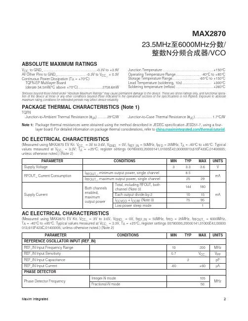
An Integrated 18 GHz fractional-N PLL in SiGe BiCMOS technology for satellite communications
- 格式:pdf
- 大小:285.31 KB
- 文档页数:4
RMO4C-4An Integrated 18 GHz Fractional-N PLL in SiGe BiCMOS Technology for Satellite CommunicationsFrank Herzel1, Sabbir A. Osmany1, Klaus Schmalz1, Wolfgang Winkler1, J. Christoph Scheytt1, Thomas Podrebersek2, Rüdiger Follmann2, and Heinz-Volker Heyer31 2IHP, Im Technologiepark 25, D-15236 Frankfurt (Oder), Germany3IMST GmbH, Carl-Friedrich-Gauß-Str. 2, D-47475 Kamp-Lintfort, Germany Kayser-Threde GmbH, Wolfrathshauser Str. 48, D-81379, Munichapproaches ground or the supply voltage, the charge pump may become very noisy, since the MOSFETs leave the saturation region. Recently, a biased dual-loop (BDL) PLL architecture was presented and verified in a 48 GHz integer-N PLL, which may solve these problems [7]. Since in a fractional-N PLL the charge pump leakage currents are significantly higher, it has been an open question up until now whether or not the principle is useful here. This paper applies the BDL concept to an 18 GHz fractional-N PLL. It shows experimentally that with proper output biasing of the dominating charge pump for VCO fine tuning, the PLL tuning range can be significantly extended without deterioration of phase noise and spurs. II. PLL ARCHITECTURE Fig. 1 shows the PLL architecture. The VCO represents a differential Colpitts oscillator with two analog tuning inputs [8]. It is followed by a 1:4 prescaler and a programmable divider interacting with the digital CMOS part of the chip. The divider output is connected to a phase-frequency detector (PFD) followed by a highcurrent charge pump (CP) named CP1 and a low-current charge pump CP2. After passing the low-pass filter (LPF), the two voltages control the output frequency of the VCO.Abstract — We present a single-chip fractional-N PLL for space applications. The design employs a high-current charge pump with optimum output biasing and a low-current charge pump for extension of the tuning range. We show that the extension of the tuning range does not increase phase noise and reference spurs. The PLL is tunable from 17.5 GHz to 18.9 GHz, and the phase noise at 1 MHz offset is below 110 dBc/Hz. Since loop bandwidth and phase noise are almost independent of the output frequency, the design is robust against parameter variations with process, voltage, temperature, and ageing. Index Terms — BiCMOS, Dual-loop PLL, PVT Tolerance, Frequency Synthesizer, Silicon-Germanium, Satellite CommunicationI. INTRODUCTION Satellite communication in the Ka-band represents a fast growing market [1]. Examples are HDTV and internetvia-satellite services such as DVB-RCS. In order to achieve low cost and high flexibility, highly integrated silicon-based solutions are desirable. A low-noise integerN PLL at 18-19 GHz has been described recently [2]. Since in integer-N PLLs the channel spacing cannot be smaller than the comparison frequency in the phase detector, they are not very flexible. Fractional-N phaselocked loops (PLL) above 10 GHz have been reported in both CMOS [3] and SiGe BiCMOS technology [4]. Silicon-Germanium HBTs compare favorably with CMOS and GaAs HBT technologies in radiation hardness [5] and flicker noise performance [6] and are perfectly suited for space. Integrated PLLs suffer from several inherent problems. First, in order to compensate device parameter variations with process and temperature as well as aging effects, the tuning range must be relatively large. This may result in a high phase noise and large reference spurs. Second, the gain variation of an integrated VCO is usually quite large making the loop bandwidth and the phase noise dependent on device parameter variations. Third, if the control voltage of the voltage-controlled oscillator (VCO)Fig. 1. Schematic view of dual-loop PLL.978-1-4244-3376-6/978-1-4244-3378-0/09/$25.00 © 2009 IEEE3292009 IEEE Radio Frequency Integrated Circuits SymposiumThe digital CMOS part of the chip contains a fractionalN sigma-delta modulator (SDM) and a serial processor interface (SPI). The number of SDM stages is switchable from one to four by using the SPI. All SDM accumulators are 40 bit wide. This allows very fine frequency steps in the mHz range to be programmed. All SPI registers have been tripled to achieve better radiation hardness [4]. The loop filter is shown in Fig. 2. The fine tuning filter is a standard PLL filter supplemented with the two bias resistors R4 and R5. This voltage divider is connected to a quiet supply voltage VCC (3.3V) and to the board ground (0V). It keeps the fine tuning voltage at a value where the gain is quite constant, resulting in a low phase noise. The filter in the coarse tuning loop is nothing but a large external capacitor CCOARSE = 100nF connected to the board ground in parallel with a MIM capacitor to chip ground.VCC R5 CP1 R4 R1 C2 C1 CP2 CC OA R SE COARSE C3 R3 FINEdivider will affect the loop dynamics and increase the noise floor. Fig. 3 shows the phase noise spectrum for different values of R4 and for the case without voltage divider. As evident from the figure, the effect of the voltage divider on the phase noise is almost negligible, if R4 is larger than 50 kΩ. Interestingly, the addition of the voltage divider to the loop filter offers the opportunity to reduce the overshoot in the phase noise spectrum. However, if the bias resistances are too small, say, below 5 kΩ, the phase noise floor will increase.Fig. 3. Analytically calculated phase noise spectrum for different values for the bias resistor R4.This trade-off results in an optimum value for the bias resistance R4 with respect to the integrated phase error.Fig. 2. Schematic of the loop filter.It can be shown that the dual-loop PLL is stable provided that CCOARSE is large enough [9]. In this case, the dynamics is completely determined by the fine tuning loop. In other words, the slow COARSE tuning loop is responsible for compensation of parameter variations with process, temperature and ageing, while the fine tuning loop suppresses the VCO noise to an acceptable level. It should be noted that the loops are always active, that is, switching is not required. This allows the PLL to remain permanently locked in the presence of temperature variations.Fig. 4. RMS phase error as a function of the bias resistance R4.III. PHASE NOISE MODELING We use an analytical linear PLL model [10] to optimize the loop filter. In order to keep the fine tuning voltage close to the noise-optimum value of 1.1 V, we use R5=2*R4 for the bias resistors. For a good biasing R4 should be small, since the charge pump leakage currents also affect the dc bias point. However, if R4 is too small, its thermal noise current will be large and the voltageThe RMS phase error is depicted in Fig. 4. It was ( /10) determined from the phase noise spectrum S φ =10 ₤ by usingσ = 180 π(°) ∫ 2S0∞φ( f )df .In the PLL circuit, we have used external resistors for experimental optimization of the phase noise. In our330design we employed a digital bondpad for reference input which contains a minimum size input inverter. This turned out to be disadvantageous due to the large noise contribution in the reference path. Figure 5 shows that a gate width of at least 10µm is required to make this noise contribution negligible at 0dBm input power. This will be considered in a future design.1.2 V. This shows that despite an increased leakage due to the high charge pump activity in a fractional-N PLL, the fine tuning voltage can be kept close to the optimum value over the whole tuning range. The reference spurs are 65dB below the carrier as shown in Fig. 9.Fig. 5. Phase noise spectrum for different sizes of the first CMOS inverter in the reference input buffer.IV. MEASUREMENTS The synthesizer was fabricated in a 0.25 µm low-cost SiGe BiCMOS technology using 21 mask steps [11]. A 2 chip photo is shown in Fig. 6. The die area is 5 mm including bondpads.Fig. 7. Phase noise spectrum at 18.00002, 18.50002 and 18.80002 GHz with VCOARSE=VFINE.Fig. 6. Chip photo of the 18 GHz PLL.Unlike in [4], we use the new BDL architecture here. The measured PLL tuning range is 1.4 GHz (from 17.5 GHz to 18.9 GHz) compared to 380 MHz in single-loop operation without coarse tuning. Fig. 7 shows the measured phase noise in single-loop configuration with FINE and COARSE connected. As expected, the phase noise is quite high due to the large VCO tuning gain. The phase noise for the BDL version is shown in Fig. 8. The phase noise at 1 MHz is below -110 dBc/Hz. This is 10 dB less than in Fig. 7, mainly due to the lower VCO gain. The close-in phase noise is relatively large, since a digital bondpad was used for the reference input as discussed in Section III. The measured fine tuning voltages for the three frequencies are between 1.15 V andFig. 8. Phase noise spectrum at 18.00002, 18.50002 and 18.80002 GHz in biased dual-loop configuration.In order to determine the noise contribution of the coarse tuning loop, we apply externally the same voltages to COARSE, which have been measured in the biased dual-loop configuration. Here, the bias resistances have been removed. The result is depicted in Fig. 10. The phase noise is not better than for the BDL configuration shown in Fig. 8. The reference spurs are also 65 dB below the carrier. This demonstrates that the addition of a slow331coarse tuning loop in conjunction with fine tuning biasing increases the tuning range without deteriorating phase noise and spurs.ACKNOWLEDGEMENT This work was supported by the European Space Agency (ESA) and the German Aerospace Center (Deutsches Zentrum für Luft- und Raumfahrt, DLR). The authors thank the IHP technology team for the fabrication of the test chip. REFERENCESC. S. Vaucher, O. Apeldoorn, M. Apostolidou, J. Dekkers, A. Farrugia, H. Gul, N. Kramer, and L. Praamsma, “SiliconGermanium ICs for Satellite Microwave Front-ends,” in Proceedings of the IEEE Bipolar/BiCMOS Circuits and Technology Meeting (BCTM2005), Santa Barbara, USA, pp. 196-203, Oct. 2005. [2] S. A. Osmany, F. Herzel, J. C. Scheytt, K. Schmalz, and W. Winkler, “An Integrated 19-GHz Low-Phase-Noise Frequency Synthesizer in SiGe BiCMOS Technology,” in Proceedings of the 29th IEEE Compound Semiconductor IC (CSIC), Portland, USA, pp. 191-194, Oct. 2007. [3] M. Tiebout, C. Sandner, H.-D. Wohlmuth, N. Da Dalt, and E. Thaller, “A Fully Integrated 13GHz ΔΣ Fractional-N PLL in 0.13 µm CMOS,” in IEEE Int. Solid-State Circuits Conf. (ISSCC) Dig. Tech. Papers, vol. 47, 2004, pp. 386-387. [4] R. Follmann, D. Köther, T. Kohl, M. Engels, V. Heyer, K. Schmalz, F. Herzel, W. Winkler, S. Osmany, and U. Jagdhold, “A Low Phase Noise Integrated SiGe 18..20 GHz Fractional-N Synthesizer,” in Proceedings of the 3rd European Microwave Integrated Circuits Conference (EuMIC2007), Munich, Germany, pp. 263-266, Oct. 2007. [5] J. D. Cressler, “SiGe HBT technology: a New Contender for Si-based RF and Microwave Circuit Applications,” IEEE Transactions on Microwave Theory and Techniques, vol. 46, pp. 572-589, May 1998. [6] G. Niu, “Noise in SiGe HBT RF Technology: Physics, Modeling, and Circuit Implementations,” Proceedings of the IEEE, vol. 93, pp. 1583-1597, Sep. 2005. [7] F. Herzel, S. Glisic, S. A. Osmany, J. C. Scheytt, K. Schmalz, W. Winkler, and M. Engels, “A Fully Integrated 48-GHz Low-Noise PLL with a Constant Loop Bandwidth,” in Proceedings of the 2008 IEEE Topical Meeting on Silicon Monolithic Integrated Circuits in RF Systems (SiRF 2008), Orlando, USA, pp. 82-85, Jan. 2008. [8] S. A. Osmany, F. Herzel, J. C. Scheytt, K. Schmalz, and W. Winkler, “Integrated 22 GHz Low-Phase-Noise VCO with Digital Tuning in SiGe BiCMOS Technology,” Electronics Letters, vol. 45, pp. 39-40, Jan. 2009. [9] F. Herzel, G. Fischer, and H. Gustat, “An Integrated CMOS RF Synthesizer for 802.11a Wireless LAN,” IEEE Journal of Solid-State Circuits, vol. 38, pp. 1767-1770, Oct. 2003. [10] S. A. Osmany, F. Herzel, K. Schmalz, and W. Winkler, “Phase Noise and Jitter Modeling for Fractional-N PLLs,” Advances in Radio Science, vol. 5, pp. 313-320, 2007. [11] D. Knoll, et al., “A Modular, Low-Cost SiGe:C BiCMOS Process Featuring High-fT and High-BVCEO Transistors,” in Proceedings of the IEEE Bipolar/BiCMOS Circuits and Technology Meeting (BCTM2004), Montreal, Canada, pp. 241-244, Sep. 2004. [1]Fig. 9. PLL output spectrum at 18.50002 GHz.Fig. 10. Phase noise spectrum at 18.00002, 18.50002 and 18.80002 GHz in single-loop configuration with external VCOARSE.V. CONCLUSION We have applied the biased dual-loop PLL concept to a fractional-N synthesizer. The tuning range of a narrowband PLL could be significantly extended keeping phase noise and spurs low. Only one of the two charge pumps contributes to the overall phase noise and is biased at optimum output voltage. This reduces charge pump mismatch over the whole tuning range. Moreover, loop bandwidth and phase noise spectrum are almost independent of the PLL output frequency. This makes the synthesizer performance robust against device parameter variations with process, voltage, temperature, and ageing.332。