
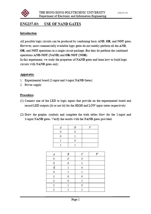
USE OF NAND GATES
- 格式:pdf
- 大小:221.50 KB
- 文档页数:5

2. Fundamentals of Logic gates2.1 LOGIC GATESWe have seen that the foundation of logic design is seated in a well defined axiomatic system called Boolean algebra, which was shown to be what is known as a“Huntington system”.In this axiomatic system the definition of AND and OR operators or functions was set forth and these were found to be well defined operators having certain properties that allow us to extend their definition to Hardware applications.These AND and OR operators,sometimes referred to as connectives, actually suggest a function that can be emulated by some H/w logic device. The logic Hardware devices just mentioned are commonly referred to as “gates”.Keep in mind that the usage of “gate” refers to an actual piece of Hardware where “function” or “operation” refers to a logic operator AND. On the other hand, when we refer to a “gate” we are referring directly to a piece of hardware called a gate. The main point to remember is ‘Don’t confuse gates with logic operators’.2.1.1 Basic Logic GatesPositive and Negative Logic DesignationThe binary signals at the inputs or outputs of any gate can have one of the two values except during transition. One signal levels represents logic 1 and the other logic 0. Since two signal values are assigned two to logic values, there exist two different assignments of signals to logic.Logics 1 and 0 are generally represented by different voltage levels. Consider the two values of a binary signal as shown in Fig. 2.5.1. One value must be higher than the other since the two values must be different in order to distinguish between them. We designate the higher voltage level by H and lower voltage level by L. There are two choices for logic values assignment. Choosing the high-level (H) to represent logic 1 as shown in (a) defines a positive logic system. Choosing the low level L to represent logic-1 as shown in (b), defines a negative logic system.Fig. 2.5.1The terms positive and negative are somewhat misleading since both signal values may be positive or both may be negative. Therefore, it is not signal polarity that determines the type of logic,but rather the assignment of logic values according to the relative amplitudes of the signals.The effect of changing from one logic designation to the other equivalent to complementing the logic functions because of the principle of duality of Boolean algebra.Gate DefinitionA‘gate’is defined as a multi-input (> 2) hardware device that has a two-level output. The output level (1–H/0–L) of the gate is a strict and repeatable function of the two-level(1–H/0–L)combinations applied to its inputs.Fig. 2.5.2shows a general model of a gate.Fig. 2.5.2 The general model of a gate.The term “logic” is usually used to refer to a decision making process. A logic gate, then, is a circuit that can decide to say yes or no at the output based upon inputs. We apply voltage as the input to any gate, therefore the Boolean (logic) 0 and 1 do not represent actual number but instead represent the state of a voltage variable or what is called its logic level. Sometimes logic 0 and logic 1 may be called as shown in table below:Table 2.5.2a.OR GateThe OR gate is sometimes called the “any or all gate”. To show the OR gate we use the logical symbol in Fig. 2.5.4(a).b.c.Fig. 2.5.4 (a) OR gate logic symbol. (b) Practical OR gate circuit.d.e. A truth-table for the ‘OR’ gate is shown below according to Fig. 2.5.4(b).The truth-table lists the switch and light conditions for the OR gate. The unique output from the OR gate is a LOW only when all inputs are low. The output column in Table (2.5.4) shows that only the first line generates a 0 while all others are 1.Table 2.5.4f.g.Fig. 2.5.4(c) shows the ways to express that input A is ORed with input B toproduce output Y.h.i.Fig. 2.5.4 (c)j.Example.Determine the output Y from the OR gate for the given input waveform shown in Fig. 2.5.4(d).k.l.Fig. 2.5.4 (d)m.Solution. The output of an OR gate is determined by realizing that it will be low only when both inputs are low at the same time. For the inputs the outputs is low only during period t2. In remaining time output is 1 as shown in Fig. 2.5.4(e).n.o.Fig. 2.5.4 (e)p.We are now familiar with AND and OR gates. At this stage, to illustrate at least in part how a word statement can be formulated into a mathematical statement (Boolean expression) and then to hardware network, consider the following example:q.Example. Utkarsha will go to school if Anand and Sawan go to school, or Anand and Ayush go to school.r.Solution. T his statement can be symbolized as a Boolean expression as follows:s.t.The next step is to transform this Boolean expression into a Hardware network and this is where AND and OR gates are used.u.v.The output of gate 1 is high only if both the inputs A and S are high (mean both Anandand Sawan go to school). This is the first condition for Utkarsha to go to school.w.The output of gate 2 is high only if both the inputs A and A.Y are high (means both Anand and Ayush go to school). This is the second condition for Utkarsha to go to school.x.According to example atleast one condition must be fullfilled in order that Utkarsha goesto school. The output of gate 3 is high when any of the input to gate 3 is high means at leastone condition is fulfilled or both the inputs to gate 3 are high means both the conditions are fulfilled.y.The example also demonstrates that Anand has to go to school in any condition otherwise Utkarsha will not go to school.z.b. AND GateThe AND gate is sometimes called the “all or nothing gate”. To show the AND gate we use the logic symbol in Fig. 2.5.3(a).This is the standard symbol to memorize and use from now on for AND gates.Fig. 2.5.3 (a) AND Gate logic symbol. (b) Practical AND gate circuit.Now, let us consider Fig. 2.5.3(b). The AND gate in this figure is connnected to input switches A and B. The output indicator is an LED. If a low voltage (Ground, GND) appears at inputs, A and B, then the output LED is not bit. This situation is illustrated in table (). Line 1 indicates that if the inputs are binary 0 and 0, then the output will be binary 0.Notice that only binary1s at both A and B will produce a binary 1 at the output.Table 2.5.3 AND Truth TableIt is a+5V compared to GNDappearing at A, B, or Y that is called a binary1or a HIGH voltage.A binary0,or Lowvoltage, is defined as a GND voltage (near0V compared to GND) appearing at A, B or Y.We are using positive logic because it takesa positive+5V to produce what we call abinary 1.The truth table is said to discribe theANDfunction.The unique output from the ANDgate is a HIGH only when all inputs are HIGH.Fig. 2.5.3 (c) shows the ways to expressthat input A is ANDed with input B to produceoutput Y.Pulsed OperationIn many applications, the inputs to a gate may be voltage that change with time betweenthe two logic levels and are called as pulsed waveforms. In studying the pulsed operation of an AND gate, we consider the inputs with respect to each other in order to determine the output level at any given time. Following example illustrates this operation:Example. Determine the output Y from the AND gate for the given input waveform shown in Fig. 2.5.3(d)..Fig. 2.5.3 (d)Solution. The output of an AND gate is determined by realizing that it will be high only when both inputs are high at the same time. For the inputs the outputs is high only during t3 period. In remaining times, the outputs is 0 as shown in Fig.2.5.3(e).Fig. 2.5.3 (e)Fig. 2.5.3 (e)c. NOT GateNOT gates are often called inverters. A NOT gate's output signal is the opposite of its input signal. Note that the symbol of the NOT gate is the same as that of the buffer, except for the small circle near its output. Small circles at input or output lines of a gate's schematic symbol denote the fact that the signal is inverted.Input OutputL HH L2.1.2 Universal GatesNAND and NOR gates. The NAND and NOR gates are widely used and are readily available from most integrated circuit manufacturers. A major reason for the widespread use of these gates is that they are both UNIVERSAL gates, universal in the sense that both can be used for AND operators,OR operators,as well as Inverter. Thus, we see that a complex digital system can be completely synthesized using only NAND gates or NOR gates.a.NAND GateThe NAND gate is a NOT AND, or an inverted AND function. The standard logic symbol for the NAND gate is shown in Fig. (2.5.7a). The little invert bubble(small circle)on the right end of the symbol means to invert the output of AND.b.Fig. 2.5.7(a)NAND gate logic symbol (b)A Boolean expression for the output of a NAND gate.Figure 2.5.7(b)shows a separate AND gate and inverter being used to produce the NAND logic function. Also notice that the Boolean expression for the AND gate, (A.B) and the NAND (A.B) a re shown on the logic diagram of Fig. 2.5.7(b).The truth-table for the NAND gate is shown in Fig. 2.5.7(c). The truth-table for the NAND gate is developed by inverting the output of the AND gate. ‘The unique output from the NAND gate is a LOW only when all inputs are HIGH.c.d.Fig. 2.5.7 (c) Truth-table for AND and NAND gates.Fig. 2.5.7 (d) shows the ways to express that input A is NANDed with input B yielding output Y.e.f.Fig. 2.5.7 (d)Example. Determine the output Y from the NAND gate from the given input waveformshown in Fig. 2.6.7 (e).g.h.Fig. 2.5.7 (e)Solution. The output of NAND gate is determined by realizing that it will be low onlywhen both the inputs are high and in all other conditions it will be high. The ouput Y isshown in Fig. 2.5.7(f).i.j.Fig. 2.5.7 (f)The NAND gate as a UNIVERSAL GateThe chart in Fig. 2.5.7(g) shows how would you wire NAND gates to create any of the other basic logic functions. The logic function to be performed is listed in the left column of the table; the customary symbol for that function is listed in the center column. In the right column, is a symbol diagram of how NAND gates would be wired to perform the logic function.k.l.Fig. 2.5.7 (g)m.The NOR gate.The NOR gate is actually a NOT OR gate or an inverted OR function.n.The standard logic symbol for the NOR gate is shown in Fig. 2.5.7(h)o.p.Fig. 2.5.7 (h) NOR gate logic symbol (i) Boolean expression for the output of NOR gate. Note that the NOR symbol is an OR symbol with a small invert bubble on the right side. The NOR function is being performed by an OR gate and an inverter in Fig. 2.5.7(i). The Boolean function for the OR function is shown(A+B),the Boolean expression for the final NOR function is (A + B).q.The truth-table for the NOR gate is shown in Fig. 2.5.7(j). Notice that the NOR gate truth table is just the complement of the output of the OR gate.The unique output from the NOR gate is a HIGH only when all inputs are LOW.r.s.Fig. 2.5.7 (j) Truth-table for OR and NOR gates.t.Figure 2.5.7(k) shows the ways to express that input A is ORed with inputB yieldingu.output Y.v.w.x.Fig. 2.5.7 (k)y.Example.Determine the output Y from the NOR gate from the given input waveform shown in Fig. 2.5.7(l).z.aa.Fig. 2.5.7 (l)bb.Solution. The output of NOR gate is determined by realizing that it will be HIGH only when both the inputs are LOW and in all other conditions it will be high. The output Y is shown in Fig. 2.5.7(m).cc.dd.Fig. 2.5.7 (m)B . NOR GateThe NOR gate as a UNIVERSAL gate.The chart in Fig. 2.5.7(n) shows how would your wire NOR gates to create any of the other basic logic functions.Fig. 2.5.7 (n)2.1.3 Coincidence gatesa.The Exclusive OR GateThe exclusive OR gate is sometimes referred to as the “Odd but not the even gate”. It is often shortend as “XOR gate”. The logic diagram is shown in Fig. 2.5.8 (a) with its Boolean expression. The symbol m eans the terms are XORed together.Fig. 2.5.8 (a)The truth table for XOR gate is shown in Fig. 2.5.8 (b). Notice that if any but not all the inputs are 1, then the output will be 1. ‘The unique characteristic of the XOR gates that it produces a HIGH output only when the odd no. of HIGH inputs are present.’Fig. 2.5.8 (b)To demonstrate this, Fig. 2.5.8 (c) shows a three input XOR gate logic symbol and the truth table Fig. 2.5.8 (d). The Boolean expression for a three input XOR gate can be written asFig. 2.5.8 (c)Fig. 2.5.8 (d)Putting the value of X, we getY = (AB + A B)C + (AB + AB).CY = AB C + A BC + A B C + ABCThe HIGH outputs are generated only when odd number of HIGH inputs are present (see T.T.)‘This is why XOR function is also known as odd function’.Fig. 2.5.8 (e) shows the ways to express that input A is XORed with input B yielding output Y.Fig. 2.5.8 (e)The XOR gate using AND OR-NOT gates.we know A B = AB + A BAs we know NAND and NOR are universal gates means any logic diagram can be made using only NAND gates or using only NOR gates.XOR gate using NAND gates only.XOR using NOR gates only.The procedure for implementing any logic function using only universal gate (only NAND gates or only NOR gates) will be treated in detail in section 2.6.Example. Determine the output Y from the XOR gate from the given input waveform shown in Fig. 2.5.8 (f).Fig. 2.5.8 (f)Solution. The output XOR gate is determined by realizing that it will be HIGH only when the odd number of high inputs are present therefore the output Y is high for time period t2 and t5 as shown in Fig. 2.5.8 (g).b.The Exclusive NOR gatec.d.The Exclusive NOR gate is sometimes reffered to as the ‘COINCIDENCE’ or‘EQUIVALENCE’gate.This is often shortened as‘XNOR’gate.The logic diagram is shown in Fig. 2.5.9 (a).e.f.Fig. 2.5.9 (a)g.Observe that it is the XOR symbol with the added invert bubble on theoutput side. The Boolean expression for XNOR is therefore, the invert of XOR function denoted by symbol O.h.i.j. The truth table for XNOR gate is shown in Fig. 2.5.9 (b).k.l.Fig. 2.5.9 (b)m.Notice that the output of XNOR gate is the complement of XOR truth table. n.‘The unique output of the XNOR gate is a LOW only when an odd number of input are HIGH’.o.p.Fig. 2.5.9 (c)q.r.Fig. 2.5.9 (d)s.To demonstrate this, Fig. 2.5.9 (c) shows a three input XNOR gate logic symbol and the truth-table 2.5.9 (d).t.Figure 2.5.9 (e) shows the ways to express that input A is XNORed with input B yieldingu.output Y.v.w.x.Fig. 2.5.9 (e)y.Now at this point, it is left as an exercise for the reader to make XNOR gate using ANDOR-NOT gates,using NAND gates only and using NOR gates only.z.Example.Determine the output Y from the XNOR gate from the given input waveform shown in Fig. 2.5.9 (f).aa.bb.Fig. 2.5.9 (f)cc.Solution.The output of XNOR gate is determined by realizing that it will be HIGH only when the even-number of high inputs are present, therefore the output Y is high for time period t2 and t5 as shown in Fig. 2.5.9 (g).dd.ee.F ig. 2.5.9 (g)ff.a.The Exclusive NOR gateThe Exclusive NOR gate is sometimes reffered to as the‘COINCIDENCE’or ‘EQUIVALENCE’ gate. This is often shortened as ‘XNOR’ gate. The logic diagram is shown in Fig. 2.5.9 (a).gg.hh.Fig. 2.5.9 (a)ii.Observe that it is the XOR symbol with the added invert bubble on the output side. The Boolean expression for XNOR is therefore, the invert of XOR function denoted by symbol O.jj.kk.ll. The truth table for XNOR gate is shown in Fig. 2.5.9 (b).mm.nn.Fig. 2.5.9 (b)oo.Notice that the output of XNOR gate is the complement of XOR truth table. pp.‘The unique output of the XNOR gate is a LOW only when an odd number of input are HIGH’.qq.rr.Fig. 2.5.9 (c)ss.tt.Fig. 2.5.9 (d)uu.To demonstrate this, Fig. 2.5.9 (c) shows a three input XNOR gate logic symbol and the truth-table 2.5.9 (d).vv.Figure 2.5.9 (e) shows the ways to express that input A is XNORed with input B yieldingww.output Y.xx.yy.zz.Fig. 2.5.9 (e)aaa.Now at this point, it is left as an exercise for the reader to make XNOR gate using ANDOR-NOT gates, using NAND gates only and using NOR gates only.bbb.Example.Determine the output Y from the XNOR gate from the given input waveform shown in Fig. 2.5.9 (f).ccc.ddd.Fig. 2.5.9 (f)eee.Solution. The output of XNOR gate is determined by realizing that it will be HIGH only when the even-number of high inputs are present, therefore the output Y is high for time period t2 and t5 as shown in Fig. 2.5.9 (g).fff.ggg.F ig. 2.5.9 (g)hhh.2.2 L OGIC DIAGRAMAre diagrams in the field of logic, used for representation and to carry out certain types of reasoning.Basic Logic Diagrams Basic logic diagrams are used to show the operation of a particular unit or component. Basic logic symbols are shown in their proper relationship so as to show operation only in the mostsimplified form possible. Figure 6-24 shows a basic logic diagram for a serial subtractor. The operation of the unit isdescribed briefly in the next paragraph. In the basic subtractor in figure 6-24, assume you want to subtract binary 011 (decimal 1) from binary 100 (decimal 4). At time I o, the 0 input at A and 1 input at B of inhibitor I1 results in a 0 output from inhibitor I1and a 1 output from inhibitor I2. The 0 output from I1and the 1 output from I2are applied to OR gate G1, producing a 1 output from G1. The 1 output from I2 is also applied to the delay line. The I output from G1 along with the 0 output from the delay line produces 1 output from I3. The 1 input from G1 and the 0 input from the delay line produce a 0 output from inhibitor I4. The 0 output from L and the 1 output from I3are applied to OR gate G2 producing a 1 output.At time t1the 0 inputs on the A and B input lines of I1produce 0 outputs from I1and I2. The 0 inputs on both input lines of OR gate G1result in a 0 output from G1. The I input applied to the delay line at time t o emerges (1 bit time delay) and is now applied to the inhibit line of 13 producing an 0 output from I3. The 1 output from the delay line is also applied to inhibitor I4, and along with the 0 output from G1produces a 1 output from I4. The I4output is recycled back into the delay line, and also applied to OR gate G2. As a result of the 0 and 1 inputs from I3, and I4, OR gate G2 produces a 1 output. At time t2, the 1 input on the A line and the 0 input on the B line of I1 produce a 1 output from I1and a 0output from I2. These outputs applied to OR gate G1produce a 1 output from G1, which is applied to 13 and I4. The delay line now produces a 1 output (recycled in at time t1), which is applied to I3 and I4. The 1 output from the delay line along with the 1 output from G1 produces a 0 output from I3. The 1 output from G1 along with the 1 output from the delay line produces a 0 output from I4. With 0 outputs from I3 and I4, OR gate G2 produces a 0 output.2.3 Truth TableA truth table shows how a logic circuit's output responds to various combinations of the inputs, using logic 1 for true and logic 0 for false. All permutations of the inputs are listed on the left, and the output of the circuit is listed on the right. The desired output can be achieved by a combination of logic gates. A truth table for two inputs is shown, but it can be extended to any number of inputs. The input columns are usually constructed in the order of binary counting with a number of bits equal to the number of inputs.This notation is useful especially if the operations are commutative, although one can additionally specify that the rows are the first operand and the columns are the second operand. This condensed notation is particularly useful in discussing multi-valued extensions of logic, as it significantly cuts down on combinatoric explosion of the number of rows otherwise needed. It also provides for quickly recognizable characteristic "shape" of the distribution of the values in the table which can assist the reader in grasping the rules more quickly.。


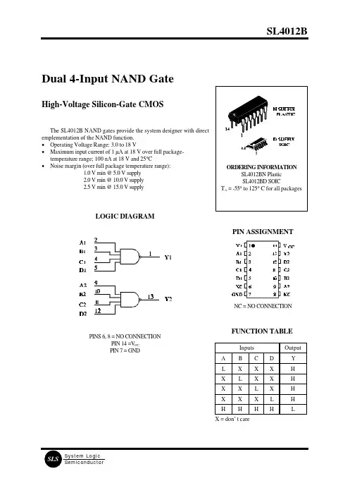
© 2005 Fairchild Semiconductor Corporation DS012408March 1995Revised January 200574LCX00 Low Voltage Quad 2-Input NAND Gate with 5V Tolerant Inputs74LCX00Low Voltage Quad 2-Input NAND Gate with 5V Tolerant InputsGeneral DescriptionThe LCX00 contains four 2-input NAND gates. The inputs tolerate voltages up to 7V allowing the interface of 5V sys-tems to 3V systems.The 74LCX00 is fabricated with advanced CMOS technol-ogy to achieve high speed operation while maintaining CMOS low power dissipation.Featuress 5V tolerant inputss 2.3V–3.6V V CC specifications provided s 5.2 ns t PD max (V CC = 3.3V), 10 µA I CC max s Power down high impedance inputs and outputs s ±24 mA output drive (V CC = 3.0V)s Implements patented noise/EMI reduction circuitry s Latch-up performance exceeds JEDEC 78 conditions s ESD performance:Human body model > 2000V Machine model > 200V s Leadless Pb-Free DQFN packageOrdering Code:Devices also available in T ape and Reel. Specify by appending the suffix letter “X ” to the ordering code.Pb-Free package per JEDEC J-STD-020B.Note 1: DQFN package available in Tape and Reel only.Note 2: “_NL ” package available in Tape and Reel only.Order Number Package Package DescriptionNumber 74LCX00M M14A 14-Lead Small Outline Integrated Circuit (SOIC), JEDEC MS-012, 0.150" Narrow 74LCX00MX_NL (Note 2)M14A Pb-Free 14-Lead Small Outline Integrated Circuit (SOIC), JEDEC MS-012, 0.150" Narrow 74LCX00SJ M14DPb-Free 14-Lead Small Outline Package (SOP), EIAJ TYPE II, 5.3mm Wide74LCX00BQX (Note 1)MLP014A Pb-Free 14-Terminal Depopulated Quad Very-Thin Flat Pack No Leads (DQFN), JEDECMO-241, 2.5 x 3.0mm 74LCX00MTC MTC1414-Lead Thin Shrink Small Outline Package (TSSOP), JEDEC MO-153, 4.4mm Wide 74LCX00MTCX_NL (Note 2)MTC14Pb-Free 14-Lead Thin Shrink Small Outline Package (TSSOP), JEDEC MO-153, 4.4mm Wide 274L C X 00Logic SymbolIEEE/IECPin DescriptionsConnection DiagramsPin Assignments for SOIC, SOP, and TSSOPPad Assignments for DQFN(Top View)Pin Names Description A n , B n Inputs O nOutputs74LCX00Absolute Maximum Ratings (Note 3)Recommended Operating Conditions (Note 5)Note 3: The Absolute Maximum Ratings are those values beyond which the safety of the device cannot be guaranteed. The device should not be operated at these limits. The parametric values defined in the Electrical Characteristics tables are not guaranteed at the Absolute Maximum Ratings. The “Recom-mended Operating Conditions ” table will define the conditions for actual device operation.Note 4: I O Absolute Maximum Rating must be observed.Note 5: Unused inputs must be held HIGH or LOW. They may not float.DC Electrical CharacteristicsSymbol ParameterValueConditionsUnits V CC Supply Voltage −0.5 to +7.0V V I DC Input Voltage −0.5 to +7.0VV O DC Output Voltage −0.5 to V CC + 0.5Output in HIGH or LOW State (Note 4)V I IK DC Input Diode Current −50V I < GND mA I OK DC Output Diode Current −50V O < GND mA +50V O > V CCI O DC Output Source/Sink Current ±50mA I CC DC Supply Current per Supply Pin ±100mA I GND DC Ground Current per Ground Pin ±100mAT STGStorage Temperature−65 to +150°CSymbol ParameterMin Max Units V CC Supply Voltage Operating 2.0 3.6V Data Retention1.5 3.6V I Input Voltage 0 5.5V V O Output Voltage HIGH or LOW State 0V CCV I OH /I OLOutput CurrentV CC = 3.0V − 3.6V ±24mAV CC = 2.7V - 3.0V ±12V CC = 2.3V - 2.7V±8T AFree-Air Operating Temperature−4085°C ∆t/∆VInput Edge Rate, V IN = 0.8V –2.0V, V CC = 3.0V10ns/VSymbol ParameterConditionsV CC T A = −40°C to +85°C Units (V)Min MaxV IH HIGH Level Input Voltage 2.3 − 2.7 1.7V 2.7 − 3.6 2.0V IL LOW Level Input Voltage 2.3 − 2.70.7V2.7 −3.60.8V OHHIGH Level Output VoltageI OH = −100 µA 2.3 − 3.6V CC − 0.2VI OH = −8 mA 2.3 1.8I OH = −12 mA 2.7 2.2I OH = −18 mA 3.0 2.4I OH = −24 mA3.0 2.2V OLLOW Level Output VoltageI OL = 100 µA 2.3 − 3.60.2V I OL = 8mA 2.30.6I OL = 12 mA 2.70.4I OL = 16 mA 3.00.4I OL = 24 mA3.00.55I I Input Leakage Current 0 ≤ V I ≤ 5.5V 2.3 − 3.6±5.0µA I OFF Power-Off Leakage Current V I or V O = 5.5V 010µA I CC Quiescent Supply Current V I = V CC or GND 2.3 − 3.610µA 3.6V ≤ V I ≤ 5.5V 2.3 − 3.6±10∆I CCIncrease in I CC per InputV IH = V CC −0.6V2.3 −3.6500µA 474L C X 00AC Electrical CharacteristicsNote 6: Skew is defined as the absolute value of the difference between the actual propagation delay for any two separate outputs of the same device. The specification applies to any outputs switching in the same direction, either HIGH-to-LOW (t OSHL ) or LOW-to-HIGH (t OSLH ).Dynamic Switching CharacteristicsCapacitanceSymbolParameterT A = −40°C to +85°CF, R L = 500ΩUnitsV CC = 3.3V ± 0.3VV CC = 2.7V V CC = 2.5V ± 0.2VC L = 50pF C L = 50pF C L = 30pF MinMax Min Max Min Max t PHL Propagation Delay1.5 5.2 1.5 6.0 1.5 6.2ns t PLH 1.55.2 1.56.01.56.2t OSHL Output to Output Skew (Note 6) 1.0ns t OSLH1.0Symbol ParameterConditionsV CC T A = 25°C Unit (V)Typical V OLP Quiet Output Dynamic Peak V OL C L = 50 pF, V IH = 3.3V, V IL = 0V 3.30.8V C L = 30 pF, V IH = 2.5V, V IL = 0V 2.50.6V OLVQuiet Output Dynamic Valley V OLC L = 50 pF, V IH = 3.3V, V IL = 0V 3.3−0.8VC L = 30 pF, V IH = 2.5V, V IL = 0V2.5−0.6Symbol ParameterConditionsTypical Units C IN Input Capacitance V CC = Open, V I = 0V or V CC 7pF C OUT Output CapacitanceV CC = 3.3V, V I = 0V or V CC8pF C PDPower Dissipation CapacitanceV CC = 3.3V, V I = 0V or V CC , f = 10 MHz25pF74LCX00AC LOADING and WAVEFORMS Generic for LCX FamilyFIGURE 1. AC Test Circuit (C L includes probe and jig capacitance)Waveform for Inverting and Non-Inverting FunctionsPropagation Delay. Pulse Width and t rec Waveforms3-STATE Output Low Enable andDisable Times for Logic3-STATE Output High Enable andDisable Times for LogicSetup Time, Hold Time and Recovery Time for Logict rise and t fallFIGURE 2. Waveforms(Input Characteristics; f =1MHz, t r = t f = 3ns)Test Switch t PLH , t PHL Opent PZL , t PLZ 6V at V CC = 3.3 ± 0.3VV CC x 2 at V CC = 2.5 ± 0.2V t PZH ,t PHZGNDSymbol V CC3.3V ± 0.3V 2.7V2.5V ± 0.2V V mi 1.5V 1.5V V CC /2V mo 1.5V 1.5V V CC /2V x V OL + 0.3V V OL + 0.3V V OL + 0.15V V yV OH − 0.3VV OH − 0.3VV OH − 0.15V 674L C X 00Schematic DiagramGeneric for LCX Family74LCX00Tape and Reel SpecificationTape Format for DQFNTAPE DIMENSIONS inches (millimeters)REEL DIMENSIONS inches (millimeters)PackageTape Number Cavity Cover Tape DesignatorSection Cavities Status Status Leader (Start End)125 (typ)Empty Sealed BQXCarrier 3000Filled Sealed Trailer (Hub End)75 (typ)EmptySealedTapeSize A B C D N W1W212 mm13.00.0590.5120.795 2.1650.4880.724(330.0)(1.50)(13.00)(20.20)(55.00)(12.4)(18.4) 874L C X 00Physical Dimensionsinches (millimeters) unless otherwise noted14-Lead Small Outline Integrated Circuit (SOIC), JEDEC MS-012, 0.150" NarrowPackage Number M14A 74LCX00Physical Dimensions inches (millimeters) unless otherwise noted (Continued)Pb-Free 14-Lead Small Outline Package (SOP), EIAJ TYPE II, 5.3mm WidePackage Number M14D 1074L C X 00Physical Dimensionsinches (millimeters) unless otherwise noted (Continued)Pb-Free 14-Terminal Depopulated Quad Very-Thin Flat Pack No Leads (DQFN), JEDEC MO-241, 2.5 x 3.0mmPackage Number MLP014APhysical Dimensions inches (millimeters) unless otherwise noted (Continued)14-Lead Thin Shrink Small Outline Package (TSSOP), JEDEC MO-153, 4.4mm WidePackage Number MTC14Fairchild does not assume any responsibility for use of any circuitry described, no circuit patent licenses are implied and Fairchild reserves the right at any time without notice to change said circuitry and specifications.LIFE SUPPORT POLICYFAIRCHILD’S PRODUCTS ARE NOT AUTHORIZED FOR USE AS CRITICAL COMPONENTS IN LIFE SUPPORT DEVICES OR SYSTEMS WITHOUT THE EXPRESS WRITTEN APPROVAL OF THE PRESIDENT OF FAIRCHILD SEMICONDUCTOR CORPORATION. As used herein:1.Life support devices or systems are devices or systemswhich, (a) are intended for surgical implant into the body, or (b) support or sustain life, and (c) whose failure to perform when properly used in accordance with instructions for use provided in the labeling, can be rea-sonably expected to result in a significant injury to the user.2. A critical component in any component of a life supportdevice or system whose failure to perform can be rea-sonably expected to cause the failure of the life support device or system, or to affect its safety or effectiveness.元器件交易网 74LCX00 Low Voltage Quad 2-Input NAND Gate with 5V Tolerant Inputs。