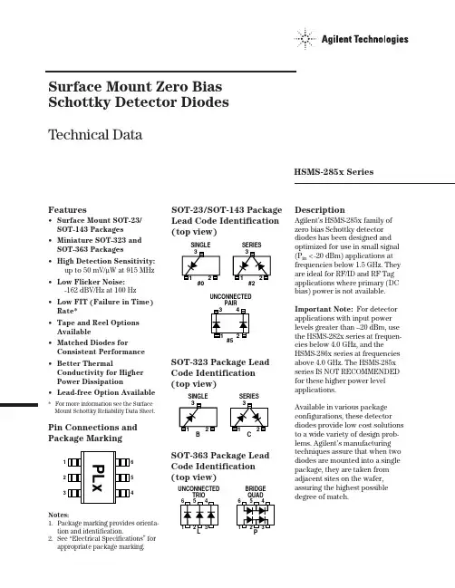
Surface Mount Zero Bias Schottky Detector Diodes Technical DataHSMS-285x SeriesSOT-23/SOT-143 Package Lead Code Identification (top view)DescriptionAgilent’s HSMS-285x family of zero bias Schottky detector diodes has been designed and optimized for use in small signal (P in <-20 dBm) applications at frequencies below 1.5GHz. They are ideal for RF/ID and RF Tag applications where primary (DC bias) power is not available.Important Note: For detector applications with input power levels greater than –20 dBm, use the HSMS-282x series at frequen-cies below 4.0 GHz, and theHSMS-286x series at frequencies above 4.0GHz. The HSMS-285x series IS NOT RECOMMENDED for these higher power level applications.Available in various package configurations, these detector diodes provide low cost solutions to a wide variety of design prob-lems. Agilent’s manufacturing techniques assure that when two diodes are mounted into a single package, they are taken from adjacent sites on the wafer,assuring the highest possible degree of match.SOT-323 Package LeadCode Identification (top view)Features•Surface Mount SOT-23/SOT-143 Packages •Miniature SOT-323 and SOT-363 Packages •High Detection Sensitivity:up to 50 mV/µW at 915 MHz •Low Flicker Noise:-162 dBV/Hz at 100 Hz •Low FIT (Failure in Time)Rate*•Tape and Reel Options Available •Matched Diodes forConsistent Performance •Better ThermalConductivity for Higher Power Dissipation •Lead-free Option Available* For more information see the Surface Mount Schottky Reliability Data Sheet.SOT-363 Package Lead Code Identification (top view)SERIES SINGLESERIESSINGLE BRIDGE QUADPUNCONNECTEDTRIOLPin Connections and Package MarkingNotes:1.Package marking provides orienta-tion and identification.2.See “Electrical Specifications” for appropriate package marking.123654SOT-23/SOT-143 DC Electrical Specifications, T C = +25°C, Single Diode Part Package Maximum Typical Number Marking Lead Forward Voltage Capacitance HSMS-Code[1]Code Configuration V F (mV)C T (pF)2850P00Single1502500.302852P22Series Pair[2,3]2855P55Unconnected Pair[2,3]Test I F = 0.1 mA I F = 1.0 mA V R = –0.5V to –1.0V Conditions f = 1 MHz Notes:1. Package marking code is in white.2. ∆V F for diodes in pairs is 15.0 mV maximum at 1.0 mA.3. ∆C T for diodes in pairs is 0.05 pF maximum at –0.5V.SOT-323/SOT-363 DC Electrical Specifications, T C = +25°C, Single Diode Part Package Maximum Typical Number Marking Lead Forward Voltage Capacitance HSMS-Code[1]Code Configuration V F (mV)C T (pF)285B P0B Single[2]1502500.30285C P2C Series Pair[2,3]285L PL L Unconnected Trio285P PP P Bridge QuadTest I F = 0.1 mA I F = 1.0 mA V R = 0.5V to –1.0V Conditions f = 1 MHz Notes:1. Package marking code is laser marked.2. ∆V F for diodes in pairs is 15.0 mV maximum at 1.0 mA.3. ∆C T for diodes in pairs is 0.05 pF maximum at –0.5V.RF Electrical Specifications, T C = +25°C, Single DiodePart Number Typical Tangential Sensitivity Typical Voltage Sensitivity Typical Video HSMS-TSS (dBm) @ f = 915 MHzγ (mV/µW) @ f = 915 MHz Resistance RV (KΩ) 2850–57408.028522855285B285C285L285PTest Video Bandwidth = 2 MHz Power in = –40 dBmConditions Zero Bias R L = 100 KΩ, Zero Bias Zero BiasEquivalent Linear Circuit ModelHSMS-285x chipSPICE ParametersParameterUnits HSMS-285xB V V 3.8C J0pF 0.18E G eV 0.69I BV A 3E -4I SA 3 E-6N 1.06R S Ω25PB (V J )V0.35P T (XTI)2M0.5Absolute Maximum Ratings, T C = +25°C, Single DiodeSymbol Parameter Unit Absolute Maximum [1]SOT-23/143SOT-323/363P IV Peak Inverse Voltage V2.0 2.0T J Junction Temperature °C 150150T STG Storage Temperature °C -65 to 150-65 to 150T OP Operating Temperature °C -65 to 150-65 to 150θjcThermal Resistance [2]°C/W500150Notes:1. Operation in excess of any one of these conditions may result in permanent damage to the device.2. T C = +25°C, where T C is defined to be the temperature at the package pins where contact is made to the circuit board.ESD WARNING:Handling PrecautionsShould Be Taken To Avoid Static Discharge.C jR j =8.33 X 10⁻⁵ nT I b + I swhereI b = externally applied bias current in ampsI s = saturation current (see table of SPICE parameters)T = temperature, °Kn = ideality factor (see table of SPICE parameters)Note:To effectively model the packaged HSMS-285x product, please refer to Application Note AN1124.R S = series resistance (see Table of SPICE parameters)C j = junction capacitance (see Table of SPICE parameters)Typical Parameters, Single DiodeFigure 1. Typical Forward Current vs. Forward Voltage.Figure 2. +25°C Output Voltage vs. Input Power at Zero Bias.Figure 3. +25°C Expanded Output Voltage vs. Input Power. See Figure 2.Figure 4. Output Voltage vs. Temperature.I F – F O R W A R D C U R R E N T (m A )00.01V F – FORWARD VOLTAGE (V)0.8 1.010010.10.2 1.8101.40.40.6 1.2 1.6V O L T A G E O U T (m V )POWER IN (dBm)V O L T A G E OU T (m V )0.3POWER IN (dBm)10130O U T P U T V O L T A G E (m V )TEMPERATURE (°C)Applications Information IntroductionAgilent’s HSMS-285x family of Schottky detector diodes has been developed specifically for low cost, high volume designs in small signal (P in < -20dBm) applica-tions at frequencies below1.5GHz. At higher frequencies, the DC biased HSMS-286x family should be considered.In large signal power or gain con-trol applications (P in>-20dBm), the HSMS-282x and HSMS-286x products should be used. The HSMS-285x zero bias diode is not designed for large signal designs. Schottky Barrier Diode CharacteristicsStripped of its package, a Schottky barrier diode chip consists of a metal-semiconductor barrier formed by deposition of a metal layer on a semiconductor. The most common of several different types, the passivated diode, is shown in Figure 5, along with its equivalent circuit.Figure 5. Schottky Diode Chip.R S is the parasitic series resistance of the diode, the sum of the bondwire and leadframe resistance, the resistance of the bulk layer of silicon, etc. RF energy coupled into R S is lost as heat—it does not contribute to the rectified output of the diode.C J is parasitic junction capaci-tance of the diode, controlled bythe thickness of the epitaxial layerand the diameter of the Schottkycontact. R j is the junctionresistance of the diode, a functionof the total current flowingthrough it.8.33 X 10-5n TR j = –––––––––––– = R V – R sI S + I b0.026= ––––– at 25°CI S + I bwheren = ideality factor (see table ofSPICE parameters)T = temperature in °KI S = saturation current (seetable of SPICE parameters)I b = externally applied biascurrent in ampsI S is a function of diode barrierheight, and can range frompicoamps for high barrier diodesto as much as 5 µA for very lowbarrier diodes.The Height of the SchottkyBarrierThe current-voltage characteristicof a Schottky barrier diode atroom temperature is described bythe following equation:V - IR SI = I S (exp (––––––) - 1)0.026On a semi-log plot (as shown inthe Agilent catalog) the currentgraph will be a straight line withinverse slope 2.3 X 0.026 = 0.060volts per cycle (until the effect ofR S is seen in a curve that droopsat high current). All Schottkydiode curves have the same slope,but not necessarily the same valueof current for a given voltage. Thisis determined by the saturationcurrent, I S, and is related to thebarrier height of the diode.Through the choice of p-type orn-type silicon, and the selection ofmetal, one can tailor the charac-teristics of a Schottky diode.Barrier height will be altered, andat the same time C J and R S will bechanged. In general, very lowbarrier height diodes (with highvalues of I S, suitable for zero biasapplications) are realized onp-type silicon. Such diodes sufferfrom higher values of R S than dothe n-type. Thus, p-type diodes aregenerally reserved for small signaldetector applications (where veryhigh values of R V swamp out highR S) and n-type diodes are used formixer applications (where highL.O. drive levels keep R V low).Measuring Diode ParametersThe measurement of the fiveelements which make up the lowfrequency equivalent circuit for apackaged Schottky diode (seeFigure 6) is a complex task.Various techniques are used foreach element. The task beginswith the elements of the diodechip itself.FOR THE HSMS-285x SERIESC P = 0.08 pFL P = 2 nHC j = 0.18 pFR S = 25 ΩR V = 9 KΩFigure 6. Equivalent Circuit of aSchottky Diode.jCROSS-SECTION OF SCHOTTKYBARRIER DIODE CHIP CIRCUITR S is perhaps the easiest tomeasure accurately. The V-I curve is measured for the diode under forward bias, and the slope of the curve is taken at some relatively high value of current (such as 5mA). This slope is converted into a resistance R d .0.026R S = R d – ––––––I fR V and C J are very difficult tomeasure. Consider the impedance of C J = 0.16 pF when measured at 1 MHz — it is approximately 1M Ω. For a well designed zero bias Schottky, R V is in the range of 5 to 25 K Ω, and it shorts out the junction capacitance. Moving up to a higher frequency enables the measurement of the capacitance,but it then shorts out the video resistance. The best measurement technique is to mount the diode in series in a 50 Ω microstrip test circuit and measure its insertion loss at low power levels (around -20 dBm) using an HP8753C network analyzer. The resulting display will appear as shown in Figure 7.I N S E R T I O N L O S S (d B )FREQUENCY (MHz)Figure 7. Measuring C J and R V .At frequencies below 10 MHz, the video resistance dominates the loss and can easily be calculated from it. At frequencies above300MHz, the junction capacitancesets the loss, which plots out as a straight line when frequency is plotted on a log scale. Again,calculation is straightforward.L P and C P are best measured on the HP8753C, with the diode terminating a 50 Ω line on the input port. The resulting tabula-tion of S 11 can be put into a microwave linear analysisprogram having the five element equivalent circuit with R V , C J and R S fixed. The optimizer can then adjust the values of L P and C P until the calculated S 11 matches the measured values. Note that extreme care must be taken to de-embed the parasitics of the 50Ω test fixture.Detector CircuitsWhen DC bias is available,Schottky diode detector circuits can be used to create low cost RF and microwave receivers with a sensitivity of -55 dBm to-57dBm.[1] These circuits can take a variety of forms, but in the mostsimple case they appear as shown in Figure 8. This is the basic detector circuit used with theHSMS-285x family of diodes.In the design of such detector circuits, the starting point is the equivalent circuit of the diode, as shown in Figure 6.Of interest in the design of the video portion of the circuit is the diode’s video impedance —the other four elements of the equiv-alent circuit disappear at all reasonable video frequencies. In general, the lower the diode’s video impedance, the better the design.RF IN The situation is somewhat more complicated in the design of the RF impedance matching network,which includes the package inductance and capacitance (which can be tuned out), the series resistance, the junction capacitance and the videoresistance. Of these five elements of the diode’s equivalent circuit,the four parasitics are constants and the video resistance is a function of the current flowing through the diode.26,000R V ≈ ––––––I S + I bwhereI S = diode saturation currentin µAI b = bias current in µA Saturation current is a function of the diode’s design,[2] and it is a constant at a given temperature.For the HSMS-285x series, it is typically 3 to 5 µA at 25°C.Saturation current sets the detec-tion sensitivity, video resistance and input RF impedance of the zero bias Schottky detector diode.[1] Agilent Application Note 923, Schottky Barrier Diode Video Detectors.[2] Agilent Application Note 969, An Optimum Zero Bias Schottky Detector Diode.Since no external bias is used with the HSMS-285x series, a single transfer curve at any given frequency is obtained, as shown in Figure2.The most difficult part of the design of a detector circuit is the input impedance matching network. For very broadband detectors, a shunt 60 Ω resistor will give good input match, but at the expense of detection sensitivity.When maximum sensitivity is required over a narrow band of frequencies, a reactive matching network is optimum. Such net-works can be realized in either lumped or distributed elements, depending upon frequency, size constraints and cost limitations, but certain general design principals exist for all types.[3] Design work begins with the RF impedance of the HSMS-285x series, which is given in Figure 9.Figure 9. RF Impedance of theHSMS-285x Series at -40dBm.915 MHz Detector Circuit Figure 10 illustrates a simple impedance matching network for a 915 MHz detector.VIDEOOUTDIMENSIONS ARE FORMICROSTRIP ON0.032" THICK FR-4.Figure 10. 915MHz MatchingNetwork for the HSMS-285x Seriesat Zero Bias.A 65 nH inductor rotates theimpedance of the diode to a pointon the Smith Chart where a shuntinductor can pull it up to thecenter. The short length of 0.065"wide microstrip line is used tomount the lead of the diode’sSOT-323 package. A shorted shuntstub of length <λ/4 provides thenecessary shunt inductance andsimultaneously provides thereturn circuit for the current gen-erated in the diode. The imped-ance of this circuit is given inFigure11.FREQUENCY (GHz): 0.9-0.93Figure 11. Input Impedance.The input match, expressed interms of return loss, is given inFigure 12.RETURNLOSS(dB)0.9-20FREQUENCY (GHz)0.915-10-150.93-5Figure 12. Input Return Loss.As can be seen, the band overwhich a good match is achieved ismore than adequate for 915 MHzRFID applications.Voltage DoublersTo this point, we have restrictedour discussion to single diodedetectors. A glance at Figure 8,however, will lead to the sugges-tion that the two types of singlediode detectors be combined intoa two diode voltage doubler[4](known also as a full wave recti-fier). Such a detector is shown inFigure 13.VIDEO OUTRF INFigure 13. Voltage Doubler Circuit.Such a circuit offers severaladvantages. First the voltageoutputs of two diodes are addedin series, increasing the overallvalue of voltage sensitivity for thenetwork (compared to a singlediode detector). Second, the RFimpedances of the two diodes areadded in parallel, making the jobof reactive matching a bit easier.[3] Agilent Application Note 963, Impedance Matching Techniques for Mixers and Detectors.[4] Agilent Application Note 956-4, Schottky Diode Voltage Doubler.[5] Agilent Application Note 965-3, Flicker Noise in Schottky Diodes.Such a circuit can easily be realized using the two series di-odes in the HSMS-285C.Flicker NoiseReference to Figure 5 will show that there is a junction of metal,silicon, and passivation around the rim of the Schottky contact. It is in this three-way junction that flicker noise [5] is generated. This noise can severely reduce the sensitivity of a crystal video receiver utilizing a Schottky detector circuit if the video frequency is below the noise corner. Flicker noise can be substantially reduced by the elimination of passivation, but such diodes cannot be mounted in non-hermetic packages. p-type silicon Schottky diodes have the least flicker noise at a given value of external bias (compared to n-type silicon or GaAs). At zero bias, such diodes can have extremely low values of flicker noise. For the HSMS-285x series,the noise temperature ratio is given in Figure 14.N O I S E T E M P E R A T U R E R A T I O (d B )FREQUENCY (Hz)Figure 14. Typical Noise Temperature Ratio.Noise temperature ratio is the quotient of the diode’s noise power (expressed in dBV/Hz) di-vided by the noise power of an ideal resistor of resistance R =R V .For an ideal resistor R, at 300°K,the noise voltage can be com-puted fromv = 1.287 X 10⁻¹⁰ √R volts/Hz which can be expressed as20 log 10 vdBV/HzThus, for a diode with R V = 9K Ω,the noise voltage is 12.2 nV/Hz or -158 dBV/Hz. On the graph of Figure 14, -158 dBV/Hz would replace the zero on the vertical scale to convert the chart to one of absolute noise voltage vs.frequency.Diode BurnoutAny Schottky junction, be it an RF diode or the gate of a MESFET, is relatively delicate and can be burned out with excessive RF power. Many crystal video receiv-ers used in RFID (tag) applica-tions find themselves in poorly controlled environments where high power sources may bepresent. Examples are the areas around airport and FAA radars,nearby ham radio operators, the vicinity of a broadcast band trans-mitter, etc. In such environments,the Schottky diodes of thereceiver can be protected by a de-vice known as a limiter diode.[6]Formerly available only in radar warning receivers and other high cost electronic warfare applica-tions, these diodes have been adapted to commercial and consumer circuits.Agilent offers a complete line of surface mountable PIN limiter diodes. Most notably, ourHSMP-4820 (SOT-23) can act as a very fast (nanosecond) power-sensitive switch when placedbetween the antenna and the Schottky diode, shorting out the RF circuit temporarily andreflecting the excessive RF energy back out the antenna.Assembly InstructionsSOT-323 PCB FootprintA recommended PCB pad layout for the miniature SOT-323 (SC-70)package is shown in Figure 15(dimensions are in inches). This layout provides ample allowance for package placement by auto-mated assembly equipment without adding parasitics that could impair the performance.Figure 16 shows the pad layout for the six-lead SOT-363.Figure 15. PCB Pad Layout (dimensions in inches).Figure 16. PCB Pad Layout (dimensions in inches).[6] Agilent Application Note 1050, Low Cost, Surface Mount Power Limiters.SMT AssemblyReliable assembly of surface mount components is a complex process that involves manymaterial, process, and equipment factors, including: method of heating (e.g., IR or vapor phase reflow, wave soldering, etc.)circuit board material, conductor thickness and pattern, type of solder alloy, and the thermalconductivity and thermal mass of components. Components with a low mass, such as the SOT packages, will reach solderreflow temperatures faster than those with a greater mass.Agilent’s diodes have beenqualified to the time-temperature profile shown in Figure 17. This profile is representative of an IR reflow type of surface mount assembly process.TIME (seconds)T E M P E R A T U R E (°C )05010015020025060120180240300Figure 17. Surface Mount Assembly Profile.After ramping up from room temperature, the circuit board with components attached to it (held in place with solder paste)passes through one or morepreheat zones. The preheat zones increase the temperature of the board and components to prevent thermal shock and begin evapo-rating solvents from the solder paste. The reflow zone briefly elevates the temperature suffi-ciently to produce a reflow of the solder.The rates of change of tempera-ture for the ramp-up and cool-down zones are chosen to be low enough to not cause deformation of the board or damage to compo-nents due to thermal shock. The maximum temperature in the reflow zone (T MAX ) should not exceed 235°C.These parameters are typical for a surface mount assembly process for Agilent diodes. As a general guideline, the circuit board and components should be exposed only to the minimum temperatures and times necessary to achieve a uniform reflow of solder.Part Number Ordering InformationNo. of Part Number Devices Container HSMS-285x-TR2*1000013" Reel HSMS-285x-TR1*30007" Reel HSMS-285x-BLK *100antistatic bagwhere x = 0, 2, 5, B, C, L and P for HSMS-285x.For lead-free option, the part number will have the character "G" at the end, eg. HSMS-285x-TR2G for a 10,000 lead-free reel.Package DimensionsOutline 23 (SOT-23)Outline 143 (SOT-143)SIDE VIEWEND VIEWDIMENSIONS ARE IN MILLIMETERS (INCHES)DIMENSIONS ARE IN MILLIMETERS (INCHES)PACKAGE MARKING CODE (XX)Outline SOT-363 (SC-70 6 Lead)Outline SOT-323 (SC-70 3 Lead)0.25 (0.010)0.15 (0.006)0.30 (0.012)0.10 (0.004)0.425 (0.017)DIMENSIONS ARE IN MILLIMETERS (INCHES)0.30 (0.012)0.10 (0.004)0.425 (0.017)DIMENSIONS ARE IN MILLIMETERS (INCHES)Device OrientationUSER FEEDFor Outline SOT-143Note: "AB" represents package marking code. "C" represents date code.END VIEWTOP VIEW For Outlines SOT-23, -323Note: "AB" represents package marking code. "C" represents date code.END VIEWTOP VIEW END VIEWTOP VIEW Note: "AB" represents package marking code. "C" represents date code.For Outline SOT-363Tape Dimensions and Product OrientationFor Outline SOT-23DESCRIPTIONSYMBOL SIZE (mm)SIZE (INCHES)LENGTH WIDTH DEPTH PITCHBOTTOM HOLE DIAMETER A 0B 0K 0P D 1 3.15 ± 0.102.77 ± 0.101.22 ± 0.104.00 ± 0.101.00 + 0.050.124 ± 0.0040.109 ± 0.0040.048 ± 0.0040.157 ± 0.0040.039 ± 0.002CAVITYDIAMETER PITCH POSITION D P 0E 1.50 + 0.104.00 ± 0.101.75 ± 0.100.059 + 0.0040.157 ± 0.0040.069 ± 0.004PERFORATIONWIDTH THICKNESSW t18.00 + 0.30 – 0.100.229 ± 0.0130.315 + 0.012 – 0.0040.009 ± 0.0005CARRIER TAPE CAVITY TO PERFORATION (WIDTH DIRECTION)CAVITY TO PERFORATION (LENGTH DIRECTION)F P 23.50 ± 0.052.00 ± 0.050.138 ± 0.0020.079 ± 0.002DISTANCE BETWEEN CENTERLINEFor Outline SOT-1431DESCRIPTIONSYMBOL SIZE (mm)SIZE (INCHES)LENGTH WIDTH DEPTH PITCHBOTTOM HOLE DIAMETER A 0B 0K 0P D 1 3.19 ± 0.102.80 ± 0.101.31 ± 0.104.00 ± 0.101.00 + 0.250.126 ± 0.0040.110 ± 0.0040.052 ± 0.0040.157 ± 0.0040.039 + 0.010CAVITYDIAMETER PITCH POSITION D P 0E 1.50 + 0.104.00 ± 0.101.75 ± 0.100.059 + 0.0040.157 ± 0.0040.069 ± 0.004PERFORATIONWIDTH THICKNESSW t18.00 + 0.30 – 0.100.254 ± 0.0130.315+ 0.012 – 0.0040.0100 ± 0.0005CARRIER TAPE CAVITY TO PERFORATION (WIDTH DIRECTION)CAVITY TO PERFORATION (LENGTH DIRECTION)F P 23.50 ± 0.052.00 ± 0.050.138 ± 0.0020.079 ± 0.002DISTANCE/semiconductorsFor product information and a complete list of distributors, please go to our web site.For technical assistance call:Americas/Canada: +1 (800) 235-0312 or (916) 788-6763Europe: +49 (0) 6441 92460China: 10800 650 0017Hong Kong: (65) 6756 2394India, Australia, New Zealand: (65) 6755 1939Japan: (+81 3) 3335-8152(Domestic/International), or 0120-61-1280(Domestic Only)Korea: (65) 6755 1989Singapore, Malaysia, Vietnam, Thailand, Philippines,Indonesia: (65) 6755 2044Taiwan: (65) 6755 1843Data subject to change.Copyright © 2004 Agilent Technologies, Inc.Obsoletes 5968-7457E March 24, 20045989-0479ENTape Dimensions and Product OrientationFor Outlines SOT-323, -363(CARRIER TAPE THICKNESS)(COVER TAPE THICKNESS)DESCRIPTIONSYMBOL SIZE (mm)SIZE (INCHES)LENGTH WIDTH DEPTH PITCHBOTTOM HOLE DIAMETER A 0B 0K 0P D 1 2.40 ± 0.102.40 ± 0.101.20 ± 0.104.00 ± 0.101.00 + 0.250.094 ± 0.0040.094 ± 0.0040.047 ± 0.0040.157 ± 0.0040.039 + 0.010CAVITYDIAMETER PITCH POSITION D P 0E 1.55 ± 0.054.00 ± 0.101.75 ± 0.100.061 ± 0.0020.157 ± 0.0040.069 ± 0.004PERFORATIONWIDTH THICKNESS W t 18.00 ± 0.300.254 ± 0.020.315 ± 0.0120.0100 ± 0.0008CARRIER TAPE CAVITY TO PERFORATION (WIDTH DIRECTION)CAVITY TO PERFORATION (LENGTH DIRECTION)F P 2 3.50 ± 0.052.00 ± 0.050.138 ± 0.0020.079 ± 0.002DISTANCEFOR SOT-323 (SC70-3 LEAD)An8°C MAX FOR SOT-363 (SC70-6 LEAD)10°C MAXANGLEWIDTHTAPE THICKNESS C T t 5.4 ± 0.100.062 ± 0.0010.205 ± 0.0040.0025 ± 0.00004COVER TAPE。