NC7WV04P6X, 规格书,Datasheet 资料
- 格式:pdf
- 大小:206.24 KB
- 文档页数:9
Supply Voltage Input Voltage (VIN) Output Voltage (VOUT) VCC = 0.0V HIGH or LOW State Output Current in IOH/IOL VCC = 3.0V to 3.6V VCC = 2.3V to 2.7V VCC = 1.65V to 1.95V VCC = 1.4V to 1.6V VCC = 1.1V to 1.3V VCC = 0.9V Free Air Operating Temperature (TA) Minimum Input Edge Rate (∆t/∆V) VIN = 0.8V to 2.0V, VCC = 3.0V 10 ns/V
TinyLogic is a registered trademark of Fairchild Semiconductor Corporation. MicroPak and Quiet Series are trademarks of Fairchild Semiconductor Corporation.
NC7WV04 TinyLogic ULP-A Dual Inverter
October 2003 Revised March 2004
NC7WV04 TinyLogic ULP-A Dual Inverter
General Description
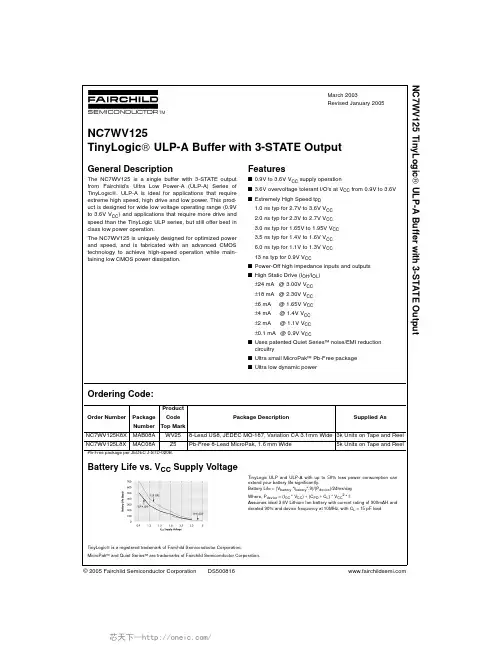
The NC7WV04 is a dual inverter from Fairchild’s Ultra Low Power-A (ULP-A) Series of TinyLogic. ULP-A is ideal for applications that require extreme high speed, high drive and low power. This product is designed for a wide low voltage operating range (0.9V to 3.6V VCC ) and applications that require more drive and speed than the TinyLogic ULP series, but still offer best in class low power operation. The NC7WV04 is uniquely designed for optimized power and speed, and is fabricated with an advanced CMOS technology to achieve high-speed operation while maintaining low CMOS power dissipation.
Ordering Code:
Order Number NC7WV04P6X NC7WV04L6X Package Number MAA06A MAC06A Product Code Top Mark V04 BA Package Description 6-Lead SC70, EIAJ SC88, 1.25mm Wide 6-Lead MicroPak, 1.0mm Wide Supplied As 3k Units on Tape and Reel 5k Units on Tape and Reel
Note 1: Absolute Maximum Ratings: are those values beyond which the safety of the device cannot be guaranteed. The device should not be operated at these limits. The parametric values defined in the Electrical Characteristics tables are not guaranteed at the absolute maximum ratings. The “Recommended Operating Conditions” table will define the conditions for actual device operation. Note 2: IO Absolute Maximum Rating must be observed. Note 3: Unused inputs must be held HIGH or LOW. They may not float.
Battery Life vs. VCC Supply Voltage
TinyLogic ULP and ULP-A with up to 50% less power consumption can extend your battery life significantly. Battery Life = (Vbattery *Ibattery*.9)/(Pdevice)/24hrs/day Where, Pdevice = (ICC * VCC) + (CPD + C L) * VCC2 * f Assumes ideal 3.6V Lithium Ion battery with current rating of 900mAH and derated 90% and device frequency at 10MHz, with CL = 15 pF load
1.10 ≤ VCC ≤ 1.30 0.65 x VCC 1.40 ≤ VCC ≤ 1.60 0.65 x VCC 1.65 ≤ VCC ≤ 1.95 0.65 x VCC 2.30 ≤ VCC < 2.70 2.70 ≤ VCC ≤ 3.60 1.6 2.0
VIL
LOW Level Input Voltage
Pad Assignments for MicroPak
(Top Thru View)
2
芯天下--/
NC7WV04
Absolute Maximum Ratings(Note 1)
Supply Voltage (VCC) DC Input Voltage (VIN) DC Output Voltage (VOUT) HIGH or LOW State (Note 2) VCC = 0V DC Input Diode Current (IIK) VIN < 0V DC Output Diode Current (IOK) VOUT < 0V VOUT > VCC DC Output Source/Sink Current (IOH/IOL) DC VCC or Ground Current per Supply Pin (ICC or Ground) Storage Temperature Range (TSTG)
0.90 1.10 ≤ VCC ≤ 1.30 1.40 ≤ VCC ≤ 1.60 1.65 ≤ VCC ≤ 1.95 2.30 ≤ VCC < 2.70 2.70 ≤ VCC ≤ 3.60
0.9V to 3.6V 0V to 3.6V 0V to 3.6V 0V to VCC
±24 mA ±18 mA ±6 mA ±4 mA ±2 mA ±0.1 mA −40°C to +85°C
DC Electrical Characteristics
Symbol VIH Parameter HIGH Level Input Voltage VCC (V) 0.90 TA = +25°C Min 0.65 x VCC Max TA = −40°C to +85°C Min 0.65 x VCC 0.65 x VCC 0.65 x VCC 0.65 x VCC 1.6 2.0 0.35 x VCC 0.35 x VCC 0.35 x VCC 0.35 x VCC 0.7 0.8 VCC − 0.1 VCC − 0.1 VCC − 0.2 VCC − 0.2 VCC − 0.2 VCC − 0.2 VCC − 0.1 VCC − 0.1 VCC − 0.2 VCC − 0.2 VCC − 0.2 VCC − 0.2 0.75 x VCC 0.75 x VCC 1.25 2.0 1.8 2.2 1.7 2.4 2.2 V IOH = −2 mA IOH = −4 mA IOH = −6 mA IOH = −12 mA IOH = −18 mA IOH = −24 mA IOH = −100 µA 0.35 x VCC 0.35 x VCC 0.35 x VCC 0.35 x VCC 0.7 0.8 V V Max Units Conditions
−0.5V to +4.6V −0.5V to +4.6V −0.5V to VCC +0.5V −0.5V to +4.6V ±50 mA −50 mA +50 mA ± 50 mA ± 50 mA −65°C to +150 °C
Recommended Operating Conditions (Note 3)
±24 mA @ 3.00V VCC ±18 mA @ 2.30V VCC ±6 mA ±4 mA ±2 mA
@ 1.65V VCC @ 1.4V VCC @ 1.1V VCC
±0.1 mA @ 0.9V VCC
s Uses patented Quiettion circuitry s Ultra small MicroPak leadfree package s Ultra low dynamic power
Features
s 0.9V to 3.6V VCC supply operation s 3.6V overvoltage tolerant I/O’s at VCC from 0.9V to 3.6V s Extremely High Speed tPD 1.5 ns typ for 2.7V to 3.6V VCC 1.8 ns typ for 2.3V to 2.7V VCC 2.0 ns typ for 1.65V to 1.95V VCC 3.2 ns typ for 1.4V to 1.6V VCC 6.0 ns typ for 1.1V to 1.3V VCC 12 ns typ for 0.9V VCC s Power-Off high impedance inputs and outputs s High Static Drive (IOH/IOL)
TinyLogic is a registered trademark of Fairchild Semiconductor Corporation. MicroPak and Quiet Series are trademarks of Fairchild Semiconductor Corporation.
NC7WV04 TinyLogic ULP-A Dual Inverter
October 2003 Revised March 2004
NC7WV04 TinyLogic ULP-A Dual Inverter
General Description
The NC7WV04 is a dual inverter from Fairchild’s Ultra Low Power-A (ULP-A) Series of TinyLogic. ULP-A is ideal for applications that require extreme high speed, high drive and low power. This product is designed for a wide low voltage operating range (0.9V to 3.6V VCC ) and applications that require more drive and speed than the TinyLogic ULP series, but still offer best in class low power operation. The NC7WV04 is uniquely designed for optimized power and speed, and is fabricated with an advanced CMOS technology to achieve high-speed operation while maintaining low CMOS power dissipation.
Ordering Code:
Order Number NC7WV04P6X NC7WV04L6X Package Number MAA06A MAC06A Product Code Top Mark V04 BA Package Description 6-Lead SC70, EIAJ SC88, 1.25mm Wide 6-Lead MicroPak, 1.0mm Wide Supplied As 3k Units on Tape and Reel 5k Units on Tape and Reel
Note 1: Absolute Maximum Ratings: are those values beyond which the safety of the device cannot be guaranteed. The device should not be operated at these limits. The parametric values defined in the Electrical Characteristics tables are not guaranteed at the absolute maximum ratings. The “Recommended Operating Conditions” table will define the conditions for actual device operation. Note 2: IO Absolute Maximum Rating must be observed. Note 3: Unused inputs must be held HIGH or LOW. They may not float.
Battery Life vs. VCC Supply Voltage
TinyLogic ULP and ULP-A with up to 50% less power consumption can extend your battery life significantly. Battery Life = (Vbattery *Ibattery*.9)/(Pdevice)/24hrs/day Where, Pdevice = (ICC * VCC) + (CPD + C L) * VCC2 * f Assumes ideal 3.6V Lithium Ion battery with current rating of 900mAH and derated 90% and device frequency at 10MHz, with CL = 15 pF load
1.10 ≤ VCC ≤ 1.30 0.65 x VCC 1.40 ≤ VCC ≤ 1.60 0.65 x VCC 1.65 ≤ VCC ≤ 1.95 0.65 x VCC 2.30 ≤ VCC < 2.70 2.70 ≤ VCC ≤ 3.60 1.6 2.0
VIL
LOW Level Input Voltage
Pad Assignments for MicroPak
(Top Thru View)
2
芯天下--/
NC7WV04
Absolute Maximum Ratings(Note 1)
Supply Voltage (VCC) DC Input Voltage (VIN) DC Output Voltage (VOUT) HIGH or LOW State (Note 2) VCC = 0V DC Input Diode Current (IIK) VIN < 0V DC Output Diode Current (IOK) VOUT < 0V VOUT > VCC DC Output Source/Sink Current (IOH/IOL) DC VCC or Ground Current per Supply Pin (ICC or Ground) Storage Temperature Range (TSTG)
0.90 1.10 ≤ VCC ≤ 1.30 1.40 ≤ VCC ≤ 1.60 1.65 ≤ VCC ≤ 1.95 2.30 ≤ VCC < 2.70 2.70 ≤ VCC ≤ 3.60
0.9V to 3.6V 0V to 3.6V 0V to 3.6V 0V to VCC
±24 mA ±18 mA ±6 mA ±4 mA ±2 mA ±0.1 mA −40°C to +85°C
DC Electrical Characteristics
Symbol VIH Parameter HIGH Level Input Voltage VCC (V) 0.90 TA = +25°C Min 0.65 x VCC Max TA = −40°C to +85°C Min 0.65 x VCC 0.65 x VCC 0.65 x VCC 0.65 x VCC 1.6 2.0 0.35 x VCC 0.35 x VCC 0.35 x VCC 0.35 x VCC 0.7 0.8 VCC − 0.1 VCC − 0.1 VCC − 0.2 VCC − 0.2 VCC − 0.2 VCC − 0.2 VCC − 0.1 VCC − 0.1 VCC − 0.2 VCC − 0.2 VCC − 0.2 VCC − 0.2 0.75 x VCC 0.75 x VCC 1.25 2.0 1.8 2.2 1.7 2.4 2.2 V IOH = −2 mA IOH = −4 mA IOH = −6 mA IOH = −12 mA IOH = −18 mA IOH = −24 mA IOH = −100 µA 0.35 x VCC 0.35 x VCC 0.35 x VCC 0.35 x VCC 0.7 0.8 V V Max Units Conditions
−0.5V to +4.6V −0.5V to +4.6V −0.5V to VCC +0.5V −0.5V to +4.6V ±50 mA −50 mA +50 mA ± 50 mA ± 50 mA −65°C to +150 °C
Recommended Operating Conditions (Note 3)
±24 mA @ 3.00V VCC ±18 mA @ 2.30V VCC ±6 mA ±4 mA ±2 mA
@ 1.65V VCC @ 1.4V VCC @ 1.1V VCC
±0.1 mA @ 0.9V VCC
s Uses patented Quiettion circuitry s Ultra small MicroPak leadfree package s Ultra low dynamic power
Features
s 0.9V to 3.6V VCC supply operation s 3.6V overvoltage tolerant I/O’s at VCC from 0.9V to 3.6V s Extremely High Speed tPD 1.5 ns typ for 2.7V to 3.6V VCC 1.8 ns typ for 2.3V to 2.7V VCC 2.0 ns typ for 1.65V to 1.95V VCC 3.2 ns typ for 1.4V to 1.6V VCC 6.0 ns typ for 1.1V to 1.3V VCC 12 ns typ for 0.9V VCC s Power-Off high impedance inputs and outputs s High Static Drive (IOH/IOL)