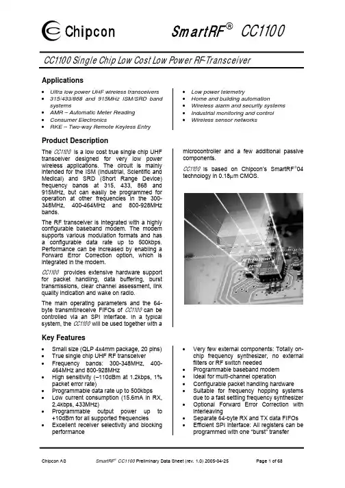
元器件交易网ChipconSmartRF ® CC1100CC1100 Single Chip Low Cost Low Power RF-TransceiverApplications• Ultra low power UHF wireless transceivers • 315/433/868 and 915MHz ISM/SRD band systems • AMR – Automatic Meter Reading • Consumer Electronics • RKE – Two-way Remote Keyless Entry • • • • • Low power telemetry Home and building automation Wireless alarm and security systems Industrial monitoring and control Wireless sensor networksProduct DescriptionThe CC1100 is a low cost true single chip UHF transceiver designed for very low power wireless applications. The circuit is mainly intended for the ISM (Industrial, Scientific and Medical) and SRD (Short Range Device) frequency bands at 315, 433, 868 and 915MHz, but can easily be programmed for operation at other frequencies in the 300348MHz, 400-464MHz and 800-928MHz bands. The RF transceiver is integrated with a highly configurable baseband modem. The modem supports various modulation formats and has a configurable data rate up to 500kbps. Performance can be increased by enabling a Forward Error Correction option, which is integrated in the modem. microcontroller and a few additional passive components.CC1100 is based on Chipcon’s SmartRF®04technology in 0.18µm CMOS.CC1100 provides extensive hardware support for packet handling, data buffering, burst transmissions, clear channel assessment, link quality indication and wake on radio.The main operating parameters and the 64byte transmit/receive FIFOs of CC1100 can be controlled via an SPI interface. In a typical system, the CC1100 will be used together with aKey Features• • • • • • • • Small size (QLP 4x4mm package, 20 pins) True single chip UHF RF transceiver Frequency bands: 300-348MHz, 400464MHz and 800-928MHz High sensitivity (–110dBm at 1.2kbps, 1% packet error rate) Programmable data rate up to 500kbps Low current consumption (15.6mA in RX, 2.4kbps, 433MHz) Programmable output power up to +10dBm for all supported frequencies Excellent receiver selectivity and blocking performance • • • • • • • • Very few external components: Totally onchip frequency synthesizer, no external filters or RF switch needed Programmable baseband modem Ideal for multi-channel operation Configurable packet handling hardware Suitable for frequency hopping systems due to a fast settling frequency synthesizer Optional Forward Error Correction with interleaving Separate 64-byte RX and TX data FIFOs Efficient SPI interface: All registers can be programmed with one “burst” transferChipcon ASSmartRF® CC1100 Preliminary Data Sheet (rev. 1.0) 2005-04-25Page 1 of 68元器件交易网ChipconFeatures (continued from front page)• • • • • • • Digital RSSI output Suited for systems compliant with EN 300 220 (Europe) and FCC CFR Part 15 (US) Wake-on-radio functionality for automatic low-power RX polling Many powerful digital features allow a high-performance RF system to be made using an inexpensive microcontroller Integrated analog temperature sensor Lead-free “green“ package Flexible support for packet oriented systems: On chip support for sync word detection, address check, flexible packet length and automatic CRC handling. Programmable channel filter bandwidth OOK and flexible ASK shaping supported 2-FSK, GFSK and MSK supported. Automatic Frequency Compensation can be used to align the frequency synthesizer to the received centre frequencySmartRF ® CC1100• • Optional automatic whitening and dewhitening of data Support for asynchronous transparent receive/transmit mode for backwards compatibility with existing radio communication protocols Programmable Carrier Sense indicator Programmable Preamble Quality Indicator for detecting preambles and improved protection against sync word detection in random noise Support for automatic Clear Channel Assessment (CCA) before transmitting (for listen-before-talk systems) Support for per-package Link Quality Indication• •• •• • • •AbbreviationsAbbreviations used in this data sheet are described below.2-FSK ADC AFC AGC AMR ASK BER CCA CRC CS DC EIRP ESR FEC FIFO FSK GFSK IF LBT LNA LO LQI MCU Binary Frequency Shift Keying Analog to Digital Converter Automatic Frequency Offset Compensation Automatic Gain Control Automatic Meter Reading Amplitude Shift Keying Bit Error Rate Clear Channel Assessment Cyclic Redundancy Check Carrier Sense Direct Current Equivalent Isotropic Radiated Power Equivalent Series Resistance Forward Error Correction First-In-First-Out Frequency Shift Keying Gaussian shaped Frequency Shift Keying Intermediate Frequency Listen Before Transmit Low Noise Amplifier Local Oscillator Link Quality Indicator Microcontroller Unit MSK PA PCB PD PER PLL PQI PQT RCOSC RF RSSI RX SAW SNR SPI TBD TX VCO WOR XOSC XTAL Minimum Shift Keying Power Amplifier Printed Circuit Board Power Down Packet Error Rate Phase Locked Loop Preamble Quality Indicator Preamble Quality Threshold RC Oscillator Radio Frequency Received Signal Strength Indicator Receive, Receive Mode Surface Aqustic Wave Signal to Noise Ratio Serial Peripheral Interface To Be Defined Transmit, Transmit Mode Voltage Controlled Oscillator Wake on Radio, Low power polling Crystal Oscillator CrystalChipcon ASSmartRF® CC1100 Preliminary Data Sheet (rev. 1.0) 2005-04-25Page 2 of 68元器件交易网ChipconTable Of Contents1 2 3 4 5 6 7 8 9 10 11 12 13 14 15 16 17 18 18.1 18.2 18.3 18.4 18.5 19 19.1 19.2 19.3 20 21 22 22.1 22.2 22.3 23 23.1 23.2 23.3 23.4 23.5 24 24.1 24.2 24.3 25 25.1 25.2 25.3 25.4 25.5 26 26.1 26.2 27 27.1SmartRF ® CC1100ABSOLUTE MAXIMUM RATINGS ...........................................................................................................5 OPERATING CONDITIONS ......................................................................................................................5 ELECTRICAL SPECIFICATIONS ...............................................................................................................6 GENERAL CHARACTERISTICS ...............................................................................................................7 RF RECEIVE SECTION...........................................................................................................................8 RF TRANSMIT SECTION ........................................................................................................................9 CRYSTAL OSCILLATOR .........................................................................................................................9 LOW POWER RC OSCILLATOR............................................................................................................10 FREQUENCY SYNTHESIZER CHARACTERISTICS ...................................................................................10 ANALOG TEMPERATURE SENSOR ........................................................................................................11 DC CHARACTERISTICS .......................................................................................................................11 POWER ON RESET...............................................................................................................................12 PIN CONFIGURATION ..........................................................................................................................12 CIRCUIT DESCRIPTION ........................................................................................................................14 APPLICATION CIRCUIT ........................................................................................................................14 CONFIGURATION OVERVIEW ..............................................................................................................16 CONFIGURATION SOFTWARE ..............................................................................................................17 4-WIRE SERIAL CONFIGURATION AND DATA INTERFACE ...................................................................18 CHIP STATUS BYTE ............................................................................................................................18 REGISTER ACCESS ..............................................................................................................................19 COMMAND STROBES ..........................................................................................................................19 FIFO ACCESS .....................................................................................................................................19 PATABLE ACCESS ............................................................................................................................19 MICROCONTROLLER INTERFACE AND PIN CONFIGURATION ...............................................................21 CONFIGURATION INTERFACE ..............................................................................................................21 GENERAL CONTROL AND STATUS PINS ..............................................................................................21 OPTIONAL RADIO CONTROL FEATURE .................................................................................................22 DATA RATE PROGRAMMING ...............................................................................................................22 RECEIVER CHANNEL FILTER BANDWIDTH..........................................................................................22 DEMODULATOR, SYMBOL SYNCHRONIZER AND DATA DECISION ......................................................23 FREQUENCY OFFSET COMPENSATION.................................................................................................23 BIT SYNCHRONIZATION ......................................................................................................................23 BYTE SYNCHRONIZATION ...................................................................................................................23 PACKET HANDLING HARDWARE SUPPORT .........................................................................................24 DATA WHITENING ...............................................................................................................................24 PACKET FORMAT ................................................................................................................................24 PACKET FILTERING IN RECEIVE MODE ...............................................................................................26 PACKET HANDLING IN TRANSMIT MODE ............................................................................................26 PACKET HANDLING IN RECEIVE MODE ..............................................................................................26 MODULATION FORMATS.....................................................................................................................27 FREQUENCY SHIFT KEYING ................................................................................................................27 MINIMUM SHIFT KEYING....................................................................................................................27 AMPLITUDE MODULATION .................................................................................................................27 RECEIVED SIGNAL QUALIFIERS AND LINK QUALITY INFORMATION ...................................................27 PREAMBLE QUALITY THRESHOLD (PQT) ...........................................................................................27 RSSI...................................................................................................................................................28 CARRIER SENSE (CS)..........................................................................................................................28 CLEAR CHANNEL ASSESSMENT (CCA) ..............................................................................................28 LINK QUALITY INDICATOR (LQI) .......................................................................................................28 FORWARD ERROR CORRECTION WITH INTERLEAVING ........................................................................29 FORWARD ERROR CORRECTION (FEC)...............................................................................................29 INTERLEAVING ...................................................................................................................................29 RADIO CONTROL ................................................................................................................................30 POWER ON START-UP SEQUENCE.........................................................................................................31Chipcon ASSmartRF® CC1100 Preliminary Data Sheet (rev. 1.0) 2005-04-25Page 3 of 68元器件交易网Chipcon27.2 27.3 27.4 27.5 27.6 27.7 28 29 30 30.1 31 32 33 34 35 36 36.1 36.2 37 37.1 37.2 37.3 38 38.1 38.2 38.3 38.4 38.5 39 40 40.1 40.2 40.3 40.4 40.5 41SmartRF ® CC1100CRYSTAL CONTROL ............................................................................................................................31 VOLTAGE REGULATOR CONTROL.......................................................................................................31 ACTIVE MODES ..................................................................................................................................31 WAKE ON RADIO (WOR) ...................................................................................................................32 TIMING ...............................................................................................................................................33 RX TERMINATION TIMER ...................................................................................................................33 DATA FIFO ........................................................................................................................................34 FREQUENCY PROGRAMMING ..............................................................................................................35 VCO...................................................................................................................................................35 VCO AND PLL SELF-CALIBRATION ...................................................................................................35 VOLTAGE REGULATORS .....................................................................................................................35 OUTPUT POWER PROGRAMMING ........................................................................................................36 CRYSTAL OSCILLATOR .......................................................................................................................37 ANTENNA INTERFACE.........................................................................................................................38 GENERAL PURPOSE / TEST OUTPUT CONTROL PINS ...........................................................................38 ASYNCHRONOUS AND SYNCHRONOUS SERIAL OPERATION ................................................................40 ASYNCHRONOUS OPERATION..............................................................................................................40 SYNCHRONOUS SERIAL OPERATION ....................................................................................................40 CONFIGURATION REGISTERS ..............................................................................................................40 CONFIGURATION REGISTER DETAILS – REGISTERS WITH PRESERVED VALUES IN SLEEP STATE ..........45 CONFIGURATION REGISTER DETAILS – REGISTERS THAT LOOSE PROGRAMMING IN SLEEP STATE ......59 STATUS REGISTER DETAILS .................................................................................................................60 PACKAGE DESCRIPTION (QLP 20)......................................................................................................63 RECOMMENDED PCB LAYOUT FOR PACKAGE (QLP 20).....................................................................64 PACKAGE THERMAL PROPERTIES ........................................................................................................64 SOLDERING INFORMATION..................................................................................................................64 TRAY SPECIFICATION ..........................................................................................................................65 CARRIER TAPE AND REEL SPECIFICATION ...........................................................................................65 ORDERING INFORMATION ...................................................................................................................65 GENERAL INFORMATION ....................................................................................................................66 DOCUMENT HISTORY .........................................................................................................................66 PRODUCT STATUS DEFINITIONS .........................................................................................................66 DISCLAIMER .......................................................................................................................................66 TRADEMARKS .....................................................................................................................................66 LIFE SUPPORT POLICY ........................................................................................................................66 ADDRESS INFORMATION .....................................................................................................................68Chipcon ASSmartRF® CC1100 Preliminary Data Sheet (rev. 1.0) 2005-04-25Page 4 of 68元器件交易网Chipcon1 Absolute Maximum RatingsSmartRF ® CC1100Under no circumstances must the absolute maximum ratings given in Table 1 be violated. Stress exceeding one or more of the limiting values may cause permanent damage to the device.Caution! ESD sensitive device. Precaution should be used when handling the device in order to prevent permanent damage. Parameter Supply voltage Voltage on any digital pin Voltage on the pins RF_P, RF_N and DCOUPL Input RF level Storage temperature range Solder reflow temperature –50 Min –0.3 –0.3 –0.3 Max 3.6 VDD+0.3, max 3.6 2.0 10 150 265 Units V V V dBm °C °C According to IPC/JEDEC J-STD-020C Condition All supply pins must have the same voltageTable 1: Absolute Maximum Ratings2Operating ConditionsMin -40 1.8 Max 85 3.6 Unit °C V All supply pins must have the same voltage ConditionThe operating conditions for CC1100 are listed Table 2 in below.Parameter Operating temperature Operating supply voltageTable 2: Operating ConditionsChipcon ASSmartRF® CC1100 Preliminary Data Sheet (rev. 1.0) 2005-04-25Page 5 of 68元器件交易网Chipcon3 Electrical SpecificationsMin Typ 900 400 90 160 Current consumption 15 MaxSmartRF ® CC1100Tc = 25°C, VDD = 3.0V if nothing else stated. Measured on Chipcon’s CC1100EM reference design. Parameter Current consumption in power down modes Unit Condition nA nA µA µA µA Voltage regulator to digital part off, register values retained, lowpower RC oscillator running (SLEEP state with WOR enabled) Voltage regulator to digital part off, register values retained (SLEEP state) Voltage regulator to digital part off, register values retained, XOSC running (SLEEP state with MCSM0.OSC_FORCE_ON set) Voltage regulator to digital part on, all other modules in power down (XOFF state) Automatic RX polling once each second, using low-power RC oscillator, with 460kHz filter bandwidth and 250kbps data rate, th PLL calibration every 4 wakeup. Average current with signal in channel below carrier sense level. Same as above, but with signal in channel above carrier sense level, 1.9ms RX timeout, and no preamble/sync word found. Automatic RX polling every 15 second, using low-power RC oscillator, with 460kHz filter bandwidth and 250kbps data rate, th PLL calibration every 4 wakeup. Average current with signal in channel below carrier sense level. Same as above, but with signal in channel above carrier sense level, 14ms RX timeout, and no preamble/sync word found. Only voltage regulator to digital part and crystal oscillator running (IDLE state) Only the frequency synthesizer running (after going from IDLE until reaching RX or TX states, and frequency calibration states) Transmit mode, +10dBm output power Transmit mode, 5dBm output power Transmit mode, 0dBm output power Transmit mode, –10dBm output power Receive mode, 2.4kbps, input at sensitivity limit Receive mode, 2.4kbps, input 30dB above sensitivity limit Receive mode, 250kbps, input at sensitivity limit Receive mode, 250kbps, input 30dB above sensitivity limit mA Transmit mode, +10dBm output power Transmit mode, 5dBm output power Transmit mode, 0dBm output power Transmit mode, –10dBm output power Receive mode, 2.4kbps, input at sensitivity limit Receive mode, 2.4kbps, input 30dB above sensitivity limit Receive mode, 250kbps, input at sensitivity limit Receive mode, 250kbps, input 30dB above sensitivity limitth34 1.8µA µA15 1.9 8.7 Current consumption, 315MHz 26.9 18.3 15.1 13.4 15.1 14.0 16.2 15.1 Current consumption, 433MHz 28.8 19.3 16.1 14.3 15.6 14.5 16.5 15.5µA mA mA mAChipcon ASSmartRF® CC1100 Preliminary Data Sheet (rev. 1.0) 2005-04-25Page 6 of 68元器件交易网ChipconParameter Current consumption, 868/915MHz Min Typ 30.3 19.7 16.6 14.0 15.4 14.2 16.2 15.2 Max mASmartRF ® CC1100Unit Condition Transmit mode, +10dBm output power Transmit mode, 5dBm output power Transmit mode, 0dBm output power Transmit mode, –10dBm output power Receive mode, 2.4kbps, input at sensitivity limit Receive mode, 2.4kbps, input 30dB above sensitivity limit Receive mode, 250kbps, input at sensitivity limit Receive mode, 250kbps, input 30dB above sensitivity limitTable 3: Electrical Specifications4General CharacteristicsMin 300 400 800 Typ Max 348 464 928 500 Unit MHz MHz MHz kbps Modulation formats supported: (Shaped) MSK (also known as differential offset QPSK) up to 500kbps 2-FSK up to 500kbps GFSK and OOK/ASK (up to 250kbps) Optional Manchester encoding (halves the data rate). Condition/NoteParameter Frequency rangeData rate1.2Table 4: General CharacteristicsChipcon ASSmartRF® CC1100 Preliminary Data Sheet (rev. 1.0) 2005-04-25Page 7 of 68元器件交易网Chipcon5 RF Receive SectionMin Typ TBD –110 –100 -88 Max Unit Ω dBm dBm dBmSmartRF ® CC1100Tc = 25°C, VDD = 3.0V if nothing else stated. Measured on Chipcon’s CC1100EM reference design. Parameter Differential input impedance Receiver sensitivity 315/433/868/915MHz Condition/Note Follow CC1100EM reference design 2-FSK, 1.2kbps, 5.2kHz deviation, 1% packet error rate, 62 bytes packet length, 58kHz digital channel filter bandwidth 2-FSK, 38.4kbps, 20kHz deviation, 1% packet error rate, 62 bytes packet length, 100kHz digital channel filter bandwidth 2-FSK, 250kbps, 127kHz deviation, 1% packet error rate, 62 bytes packet length, 540kHz digital channel filter bandwidth OOK, 250kbps OOK, 1% packet error rate, 62 bytes packet length, 540kHz digital channel filter bandwidth-88 Saturation Digital channel filter bandwidth Adjacent channel rejection, 868MHz 58 –15 650dBm dBm kHzUser programmable. The bandwidth limits are proportional to crystal frequency (given values assume a 26.0MHz crystal). 2-FSK, 38.4kbps, 20kHz deviation, 1% packet error rate, 62 bytes packet length, 100kHz digital channel filter, 150kHz channel spacing Desired channel 3dB above the sensitivity limit.23dBAlternate channel rejection, 868MHz33dB2-FSK, 38.4kbps, 20kHz deviation, 1% packet error rate, 62 bytes packet length, 100kHz digital channel filter, 150kHz channel spacing Desired channel 3dB above the sensitivity limit.Image channel rejection, 868MHz29dB2-FSK, 38.4kbps, 20kHz deviation, 1% packet error rate, 62 bytes packet length, 100kHz digital channel filter, 150kHz channel spacing, IF frequency 305kHz Desired channel 3dB above the sensitivity limit.Blocking at 1MHz offset, 868MHz Blocking at 2MHz offset, 868MHz Blocking at 5MHz offset, 868MHz Blocking at 10MHz offset, 868MHz Spurious emissions52 54 61 64 –57 –47dB dB dB dB dBm dBmDesired channel 3dB above the sensitivity limit. Compliant to ETSI EN 300 220 class 2 receiver requirement. Desired channel 3dB above the sensitivity limit. Compliant to ETSI EN 300 220 class 2 receiver requirement. Desired channel 3dB above the sensitivity limit. Compliant to ETSI EN 300 220 class 2 receiver requirement. Desired channel 3dB above the sensitivity limit. Compliant to ETSI EN 300 220 class 2 receiver requirement. 25MHz – 1GHz Above 1GHzTable 5: RF Receive SectionChipcon ASSmartRF® CC1100 Preliminary Data Sheet (rev. 1.0) 2005-04-25Page 8 of 68元器件交易网Chipcon6 RF Transmit SectionSmartRF ® CC1100Tc = 25°C, VDD = 3.0V, +10dBm if nothing else stated. Measured on Chipcon’s CC1100EM reference design. Parameter Differential load impedance Output power, highest setting Min Typ TBD 10 Max Unit Ω dBm Condition/Note Follow CC1100EM reference design Output power is programmable, and full range is available in all frequency bands. Delivered to a 50Ω single-ended load via Chipcon reference RF matching network. Output power, lowest setting –30 dBm Output power is programmable, and full range is available in all frequency bands. Delivered to a 50Ω single-ended load via Chipcon reference RF matching network. Spurious emissions and harmonics, 433/868MHz –36 –54 –47 dBm dBm dBm 25MHz – 1GHz 47-74, 87.5-118, 174-230, 470-862MHz 1800MHz-1900MHz (restricted band in Europe), when the nd operating frequency is below 900MHz (2 harmonic can not fall within this band when used in Europe) Otherwise above 1GHz <200µV/m at 3m below 960MHz. <500µV/m at 3m above 960MHz. 2 , 3 and 4 harmonic when the output power is maximum 6mV/m at 3m. (-19.6dBm EIRP) 5 harmonic 2 harmonic 3 , 4 and 5 harmonicrd th th nd th nd rd th–30 Spurious emissions, 315/915MHz -49.2 -41.2 Harmonics 315MHz -20dBm dBm EIRP dBm EIRP dBc-41.2 Harmonics 915MHz -20 -41.2dBm dBc dBmTable 6: RF Transmit Parameters7Crystal OscillatorTc = 25°C @ VDD = 3.0 V if nothing else is stated. Parameter Crystal frequency Tolerance Min 26 Typ 26 ±40 Max 27 Unit MHz ppm This is the total tolerance including a) initial tolerance, b) aging and c) temperature dependence. The acceptable crystal tolerance depends on RF frequency and channel spacing / bandwidth. ESR Start-up time 300 100 Ω µs Measured on Chipcon’s CC1100EM reference design. This parameter is to a large degree crystal dependent. Condition/NoteTable 7: Crystal Oscillator ParametersChipcon ASSmartRF® CC1100 Preliminary Data Sheet (rev. 1.0) 2005-04-25Page 9 of 68元器件交易网Chipcon8 Low Power RC OscillatorSmartRF ® CC1100Typical performance is for Tc = 25°C @ VDD = 3.0 V if nothing else is stated. The values in the table are simulated results and will be updated in later versions of the data sheet. Parameter Calibrated frequency Frequency accuracy after calibration Temperature coefficient Supply voltage coefficient Initial calibration time +0.4 +3 2 Min 34.6 Typ 34.7 Max 36 ±0.2 Unit kHz % % / °C %/V ms Frequency drift when temperature changes after calibration Frequency drift when supply voltage changes after calibration When the RC Oscillator is enabled, calibration is continuously done in the background as long as the crystal oscillator is running. Programmable, dependent on XTAL frequency Condition/Note Calibrated RC Oscillator frequency is XTAL frequency divided by 750Wake-up period58e-659650SecondsTable 8: RC Oscillator parameters9Frequency Synthesizer CharacteristicsTc = 25°C @ VDD = 3.0 V if nothing else is stated. Measured on Chipcon’s CC1100EM reference design. Parameter Programmed frequency resolution Synthesizer frequency tolerance PLL turn-on / hop time Min 397 Typ FXOSC/ 16 2 ±40 Max 412 Unit Hz Condition/Note 26MHz-27MHz crystal. The resolution (in Hz) is equal for all frequency bands. ppm Given by crystal used. Required accuracy (including temperature and aging) depends on frequency band and channel bandwidth / spacing. Time from leaving the IDLE state until arriving in the RX, FSTXON or TX state, when not performing calibration. Crystal oscillator running. Settling time for the 1xIF frequency step from RX to TX, and vice versa. Calibration can be initiated manually, or automatically before entering or after leaving RX/TX. Min/typ/max time is for 27/26/26MHz crystal frequency.80µsPLL RX/TX and TX/RX settling time PLL calibration time 0.69 18739 0.7210µs XOSC cycles0.72msTable 9: Frequency Synthesizer ParametersChipcon ASSmartRF® CC1100 Preliminary Data Sheet (rev. 1.0) 2005-04-25Page 10 of 68。