铁基超导体
- 格式:doc
- 大小:468.00 KB
- 文档页数:12

第1篇一、引言超导材料在电力、交通运输、医疗等领域具有广泛的应用前景,其优异的性能吸引了全球科学家的广泛关注。
然而,目前商业化的超导材料均为低温超导材料,需要低温环境才能发挥其超导性能。
室温超导材料的研发,将极大推动超导技术的发展和应用。
本文将从理论、实验和材料制备等方面,探讨室温超导的解决方案。
二、室温超导理论1. 电子配对机制室温超导材料的实现,首先需要解决电子配对机制问题。
目前,已知的低温超导材料主要基于电子配对机制,如BCS理论。
在室温条件下,需要寻找新的电子配对机制,以实现室温超导。
2. 电子-声子相互作用在低温超导材料中,电子-声子相互作用是超导现象的关键因素。
然而,在室温条件下,声子能量较高,电子-声子相互作用相对较弱。
因此,在室温超导材料中,需要寻找新的相互作用机制,如电子-电子相互作用、电子-磁相互作用等。
3. 电子能带结构室温超导材料的电子能带结构对超导性能有重要影响。
在室温条件下,需要寻找具有合适能带结构的材料,以满足超导条件。
三、室温超导实验1. 室温铁基超导材料近年来,铁基超导材料的研究取得了显著进展。
这类材料在室温下具有超导性能,但其超导机理尚不明确。
目前,研究人员正在探索铁基超导材料的电子配对机制、电子-声子相互作用等因素,以期揭示室温铁基超导材料的奥秘。
2. 室温钙钛矿超导材料钙钛矿超导材料在室温下具有超导性能,但其超导机理尚不明确。
研究人员通过调整钙钛矿材料的化学组成、结构等,试图实现室温超导。
3. 室温有机超导材料有机超导材料在室温下具有超导性能,但其超导机理尚不明确。
研究人员通过研究有机超导材料的电子结构、分子结构等因素,试图揭示其室温超导机理。
四、室温超导材料制备1. 量子点超导材料量子点超导材料具有独特的电子结构,有望实现室温超导。
制备量子点超导材料,需要采用纳米技术,通过控制量子点的尺寸、形状等,实现室温超导。
2. 纳米线超导材料纳米线超导材料具有优异的性能,有望实现室温超导。

超导材料有哪些
超导材料是一种在低温下能够表现出完全零电阻和完全抗磁性的材料。
自从超
导现象首次被发现以来,科学家们一直在努力寻找新的超导材料,并不断探索其在能源、电子学和医学领域的应用。
那么,超导材料究竟有哪些呢?本文将对目前已知的超导材料进行介绍。
首先,最经典的超导材料莫过于铅和汞。
这两种金属在低温下能够表现出完全
的超导性,是最早被人们发现的超导材料。
然而,由于其需要极低的工作温度,因此在实际应用中受到了一定的限制。
随着科学技术的不断进步,人们发现了一系列复合超导体,其中最著名的要数YBCO和BSCCO。
这两种复合超导体在液氮温度下即可表现出超导性,因此在实
际应用中具有更大的潜力。
YBCO和BSCCO的发现,为超导材料的应用带来了新
的希望。
除了金属和复合超导体,还有一类新型的超导材料被人们所关注,那就是铁基
超导体。
铁基超导体因其晶格结构与高温超导性的关系而备受关注,其超导转变温度较高,因此在实际应用中具有很大的潜力。
此外,还有一些其他的超导材料,如镁二硼化镁、铜氧化物等,这些材料因其
特殊的晶格结构和电子态而表现出超导性。
虽然这些材料在实际应用中面临一些挑战,但它们的发现为超导材料的研究开辟了新的方向。
总的来说,超导材料种类繁多,包括金属、复合超导体、铁基超导体等。
每一
种超导材料都有其独特的性质和潜在的应用价值,因此对超导材料的研究仍然具有重要意义。
未来,随着科学技术的不断进步,相信会有更多新型的超导材料被发现,为人类社会带来更多的惊喜和改变。
超导临界温度的最高纪录超导材料是一类具有极低电阻和强电磁场排斥特性的材料,它们在低温条件下表现出超导现象。
超导临界温度是一个重要的指标,它反映了超导材料在何种温度下可以表现出超导性质。
本文将介绍超导临界温度的最高纪录,并探讨其背后的科学原理和应用前景。
铜基和铁基超导体是已知具有最高超导临界温度的两类材料。
1993年,铜基超导体La2-xSrxCuO4创造了当时的最高纪录,其超导临界温度达到了约40K。
而在2008年,铁基超导体LaFeAsO1-xFx的发现打破了这一纪录,将超导临界温度提升到了约55K。
这一突破引起了全球科学界的广泛关注。
随后的研究工作又相继发现了一系列具有更高超导临界温度的铁基超导体,其中最高的记录是2015年发现的H3S,其超导临界温度高达203K。
超导材料之所以能够具备这样高的超导临界温度,是因为它们具有特殊的电子结构和晶格结构。
在超导材料中,电子之间通过库仑相互作用形成了一对对偶的电子态,称为库珀对。
这些库珀对在超导材料中可以自由运动而不受到散射的影响,从而产生了超导现象。
而超导临界温度则取决于材料中的电子结构和晶格结构,以及外界对材料的影响。
铜基超导体的超导临界温度之所以较高,是因为它们的电子结构中存在着铜氧层。
这种铜氧层中的电子具有特殊的能带结构,使得它们能够形成稳定的库珀对。
而铁基超导体的超导临界温度之所以更高,是因为它们的晶格结构中存在着铁砷层。
这种铁砷层中的电子同样具有特殊的能带结构,从而促使库珀对的形成。
不过,目前对于铁基超导体的超导机制仍存在争议,科学家们正在继续研究中寻找答案。
超导临界温度的提升对于超导技术的发展具有重要意义。
超导材料在电力输送、电子器件和磁共振成像等领域具有广泛的应用前景。
超导电缆可以实现高效率的电力输送,超导电子器件可以实现低功耗的电子设备,而超导磁共振成像可以提供更高分辨率的医学影像。
因此,提高超导临界温度可以进一步推动超导技术的发展,促进其在实际应用中的推广和应用。

常温超导体引言超导体是一种特殊的材料,其在低温下可以表现出完全无电阻的特性。
然而,过去的几十年里,研究人员一直致力于寻找一种在常温下表现出超导特性的材料。
如果能够找到这种常温超导体,将会对能源传输、电子设备等领域产生重大影响。
本文将介绍常温超导体的概念、研究进展以及未来的发展方向。
常温超导体的概念超导体的关键特性是它们在超导转变温度下,电阻突然变为零。
按照传统的理解,超导体只能在非常低的温度下才能表现出这种特性(通常在几个开尔文以下)。
但随着对材料科学的研究不断深入,人们意识到可能存在一些材料,在常温下也能表现出超导特性。
研究进展近年来,研究人员在寻找常温超导体方面取得了一些重要进展。
其中最引人注目的是铜基和铁基超导体的发现。
在1986年,铜基超导体的发现引起了学术界的广泛关注。
这些材料在低温下表现出非常高的超导转变温度,在77开尔文左右。
尽管这个温度仍然很低,但相比于之前的超导体材料而言,已经是一大突破。
随着对铜基超导体的研究深入,科学家们发现了铁基超导体。
这些超导体具有更高的超导转变温度,在100开尔文以上。
铁基超导体的出现给人们带来了希望,因为它们的超导转变温度接近室温。
然而,铁基超导体的研究仍处于起步阶段,目前仍然存在很多未解之谜。
未来的发展方向尽管在常温超导体的研究中取得了一些重要进展,但目前还没有找到真正的常温超导体。
因此,未来的研究方向主要集中在以下几个方面:1. 寻找新的材料:科学家们正在积极寻找能够在常温下表现出超导特性的新材料。
他们通过结构优化、掺杂和压力调控等手段来改变材料的电子结构,以寻找可能的常温超导体候选物质。
2. 解决材料失超问题:目前,铁基超导体在高温下会发生失超现象,这限制了其应用。
研究人员正致力于解决这个问题,通过调制材料的晶格结构和控制电荷传输来提高超导性能和稳定性。
3. 理解超导机制:虽然对于铜基和铁基超导体的研究取得了一些重要成果,但我们对超导机制的理解仍然有限。

低温超导工艺流程低温超导是一种在极低温下材料表现出无电阻和完全磁场排斥的现象。
这一特性使得低温超导在能源传输、磁共振成像、磁力传感器等领域具有广泛的应用前景。
下面将介绍低温超导的工艺流程。
1. 材料选择:低温超导材料主要包括铜氧化物和铁基超导体。
铜氧化物超导体具有较高的临界温度,但制备过程复杂;铁基超导体制备相对简单,但临界温度较低。
根据具体应用需求,选择合适的超导材料。
2. 高纯度材料制备:超导材料的制备需要高纯度的原料。
通常采用化学合成、固相反应或溶胶-凝胶法等方法制备超导材料的前体粉末。
然后通过高温烧结、等离子喷涂等工艺,得到高纯度、致密的超导材料。
3. 样品制备:将超导材料粉末与适量的绑定剂混合,经过球磨、成型等工艺制备成具有一定形状的样品。
制备过程中需要注意避免杂质的引入,保证样品的纯度。
4. 热处理:将样品进行热处理,目的是消除内部应力,提高材料的超导性能。
热处理过程中需要控制温度和时间,以确保样品的质量。
5. 低温冷却:将样品放置于低温环境中,通常使用液氮或液氦进行冷却。
低温冷却是实现超导态的关键步骤,必须保持低温稳定。
6. 电性能测试:对制备好的样品进行电性能测试,包括电阻测量、临界温度测量等。
通过测试结果评估样品的超导性能。
7. 封装与保护:将超导样品进行封装和保护,以防止氧化和机械损伤。
封装材料通常选择具有良好绝缘性能的材料。
8. 应用系统集成:将超导样品集成到具体的应用系统中。
根据不同的应用需求,设计和制造相应的电路和设备。
9. 系统调试与优化:对整个超导系统进行调试和优化,确保系统的稳定性和性能。
低温超导工艺流程的实施需要严格的操作规范和高水平的技术支持。
随着超导材料和工艺的不断发展,低温超导技术将在能源、医疗、通信等领域发挥更大的作用。

为什么超导体需要极低温度?
超导体需要极低温度的原因是因为超导电性只在低温下才能被观察到。
这与超导体内部的电子行为以及材料的特性有关。
超导电性的机制是通过电子-电子相互作用而形成的。
在常规金属中,电子受到晶格振动的干扰,导致电阻产生。
然而,在足够低的温度下,当超导体的电子凝结成电子对时,由于库伯对的对称性和相互作用的强度,电子对可以通过晶格中的正电荷形成一个相干的状态,从而导致电阻为零。
电子对的形成取决于电子之间的相互作用和能级分布。
在较高的温度下,热能足以破坏电子对的稳定性,使之解离成单个电子,从而导致电阻产生。
为了使电子对保持稳定,降低温度是必要的。
特定超导体的临界温度(临界温度是超导性消失的温度)是由其特定的电子-电子相互作用和能带结构决定的。
一些高温超导体(例如铜基和铁基超导体)能在相对较高的温度下实现超导性,临界温度可达到液氮温度(77开尔文或-196摄氏度)。
而传统的低温超导体(如铅、铝、铌等)则需要更低的温度,通常在液氦温度(4开尔文或-269摄氏度)以下。
因此,为了观察和利用超导性,超导体需要被冷却到极低温度条件下,以使电子对能够稳定存在并导致电阻为零。

超导材料的制备方法及步骤详解引言超导材料是一种在低温下具有零电阻和完全磁通排斥的材料。
它们在能源传输、磁共振成像、电子器件等领域具有广泛的应用前景。
本文将详细介绍超导材料的制备方法及步骤,以帮助读者深入了解超导材料的制备过程。
一、超导材料的基本概念超导材料是指在低温下电阻为零的材料。
它们具有特殊的电子结构和能带特性,使得电子在晶格中的传输不受散射的影响,从而产生零电阻的效应。
超导材料的制备过程主要包括材料选择、样品制备和性能测试三个步骤。
二、超导材料的选择超导材料的选择是超导材料制备的第一步。
目前常见的超导材料主要有铜氧化物、铁基超导体和镁二硼等。
选择合适的超导材料需要考虑其超导转变温度、结构稳定性、制备难度等因素。
铜氧化物超导体具有较高的转变温度,但制备过程复杂;铁基超导体具有较高的转变温度和较好的结构稳定性,但制备难度较大;镁二硼超导体具有较低的转变温度,但制备相对简单。
因此,在实际应用中需要根据具体需求选择合适的超导材料。
三、超导材料的样品制备超导材料的样品制备是超导材料制备的核心步骤。
样品制备的方法主要包括固相法、溶胶-凝胶法、物理气相沉积法等。
下面将详细介绍这些方法的步骤及特点。
1. 固相法固相法是超导材料制备中最常用的方法之一。
其步骤主要包括材料混合、球磨、压制和烧结等。
首先,将所需的超导材料粉末按一定比例混合,并进行球磨,以提高材料的均匀性和活性。
然后,将混合粉末压制成块状,并进行烧结,使粉末颗粒结合成致密的样品。
固相法的优点是制备过程相对简单,适用于大规模生产;缺点是制备出的样品晶粒尺寸较大,导致超导性能下降。
2. 溶胶-凝胶法溶胶-凝胶法是一种通过溶胶和凝胶的形成过程制备超导材料的方法。
其步骤主要包括溶胶制备、凝胶形成、干燥和烧结等。
首先,将超导材料的前体溶解在适当的溶剂中,形成溶胶。
然后,通过控制溶胶的温度和浓度,使其形成凝胶。
接下来,将凝胶进行干燥,以去除溶剂。
最后,进行烧结,使凝胶转变为致密的样品。

超导材料的特性与选择指南引言超导材料是一类具有特殊电性质的材料,其在低温下能够展现出零电阻和完全磁场排斥的特性。
这使得超导材料在能源传输、磁共振成像、粒子加速器等领域具有广泛的应用前景。
然而,不同类型的超导材料具有不同的特性和适用范围,因此在选择超导材料时需要考虑多个因素。
本文将介绍超导材料的基本特性,并提供一个选择指南,帮助读者了解不同超导材料的优缺点,以便更好地选择适合自己需求的超导材料。
一、超导材料的基本特性1. 零电阻:超导材料在超导态下具有零电阻特性,电流可以无阻力地通过材料中传输,这使得超导材料在能源传输和电路应用中具有重要意义。
2. 完全磁场排斥:超导材料在超导态下对磁场表现出完全排斥的特性,即磁场无法穿透超导材料,这使得超导材料在磁共振成像和磁悬浮等领域具有广泛应用。
3. 临界温度:超导材料的超导态只在低温下才能实现,其临界温度是指超导态开始出现的温度。
不同超导材料的临界温度范围不同,对于实际应用来说,需要选择适合工作温度的超导材料。
4. 临界电流密度:超导材料在超导态下能够承受的最大电流密度称为临界电流密度,该参数决定了超导材料在实际应用中的承载能力。
5. 磁化率:超导材料的磁化率是指在超导态下,材料对外加磁场的响应程度。
磁化率的大小决定了超导材料对外磁场的敏感程度。
二、超导材料的分类与特性根据超导机制的不同,超导材料可以分为传统超导材料和高温超导材料两类。
1. 传统超导材料传统超导材料是指临界温度较低的超导材料,其超导机制主要由电子与晶格振动相互作用引起。
常见的传统超导材料包括铅、锡、铟等。
铅是一种常见的传统超导材料,其临界温度约为7.2K。
铅具有良好的超导特性,但其临界电流密度较低,限制了其在高电流应用中的使用。
锡是另一种常见的传统超导材料,其临界温度约为3.7K。
锡的超导特性较铅略差,但其临界电流密度较高,适合一些需要承载较大电流的应用。
铟是一种具有较高临界温度的传统超导材料,其临界温度约为3.4K。

高温超导技术的突破和应用高温超导技术自1986年首次被发现以来,一直是科学研究和应用开发的重要领域。
超导现象是指某些材料在低于特定临界温度时电阻降为零,并且能排斥磁场,形成“迈斯纳效应”。
传统的超导材料需要在极低的温度下才能实现超导状态,而高温超导则使得常见的氮气或氦气冷却条件成为可能,使其在更广泛的应用中展现出潜力。
本文将深入探讨高温超导技术的重大突破及其应用前景。
高温超导材料的发展高温超导的关键在于材料的选择与综合,直到1986年,贝尔实验室的约瑟夫·阿尔维和他的同事们发现了掺铋铁氧化物(如YBa2Cu3O7-x)显示出高于液氮沸点(77K)下的超导性,标志着高温超导时代的到来。
这一发现引发了全球范围内对高温超导材料的研发热潮,许多不同类型的高温超导材料相继被提出和合成。
铜氧化物超导体铜氧化物类材料是最早被研究并证明具有高温超导性的材料。
具体包括钇钡铜氧化物(YBCO)、镧钡铜氧化物(LBCO)等。
其材料结构中的铜-氧平面为电子对形成提供了良好的环境,使得这些材料在较高温度下仍能表现出良好的超导特性。
铁基超导体另一类重要的高温超导材料是铁基超导体。
自从2008年首次发现后,这类材料因其多样化的化学组成与复杂的晶体结构,吸引了众多研究者的关注。
铁基超导体拥有较高的临界温度以及良好的电磁特性。
高温超导技术的重要突破临界温度的提高2019年,中国科学技术大学的研究小组成功制备出一种新型氢化物(LaH10),在接近室温(大约15摄氏度)条件下展现出高温超导性。
这一重大突破打破了之前对于临界温度限制的认识,极大地推动了高温超导技术的发展。
量子信息技术中的应用量子计算机的发展离不开高温超导技术。
利用高温超导体构建量子比特(qubit)成为量子计算的重要路径之一。
在这一领域,一些公司如IBM和Google已经开展了相关研究和项目,通过使用高度集成的高温超导电路来有效进行量子计算。
储能系统和电力传输高温超导材料在电力传输中的应用前景十分广阔。

超导材料中的超导现象与库珀对超导材料中的超导现象与库珀对是固态物理学中的两个重要概念。
超导现象指的是某些物质在低温下,电阻突然消失并表现出零电阻的特殊性质。
而库珀对则是超导现象的重要解释之一,它是一对相互作用的电子,通过库珀对的配对形成超导电流。
超导现象的研究始于20世纪初,最早被观察到的超导体是汞在4.2K以下的超导性。
这项伟大的发现使得科学家开始对超导现象产生浓厚的兴趣,并努力寻找更高温度下的超导体。
库珀对的概念是由约翰·巴丁·库珀于1956年提出的,他认为低温下的超导电流不是由独立的电子携带的,而是由成对的电子共同携带。
那么,为什么只有在低温下才能观察到超导现象呢?这是因为超导态需要满足一定的条件,其中最重要的是电子之间存在着有效的相互作用。
在高温下,周围的热运动会扰乱电子之间的相互作用,使得库珀对无法稳定地形成。
而在低温下,电子的运动能够被降低,使得库珀对能够在晶体中形成。
那么,什么是库珀对呢?库珀对是一对相互作用的电子,它们通过库珀对的配对形式来共同携带超导电流。
库珀对的形成可以通过凝聚态物理学中的“库珀对形成机制”来解释。
这个机制认为,在低温下,晶体中的正空穴和负电子之间存在一种相互吸引的相互作用力,这种吸引力被称为“库珀对结合能”。
当这种结合能大于外界的扰动能量时,库珀对就能形成。
库珀对的形成使得超导体表现出零电阻的特性。
当电子在超导体中流动时,它们不会与晶格离子或杂质散射,从而导致电阻的产生。
这是因为库珀对在晶体中移动时几乎不和其他粒子相互作用,从而减少了电子的散射过程。
这种无电阻的特性使得超导体在电力输送和磁学应用等领域具有重要的应用价值。
除了超导现象中的库珀对,研究人员还发现了一些新的超导现象。
例如,铁基超导体是一类具有高临界温度的超导体,其超导机制与库珀对有所不同。
在铁基超导体中,超导现象的产生与铁磁有序相之间的竞争有关。
通过控制铁磁有序相的出现与消失,人们可以调控铁基超导体的超导性质。
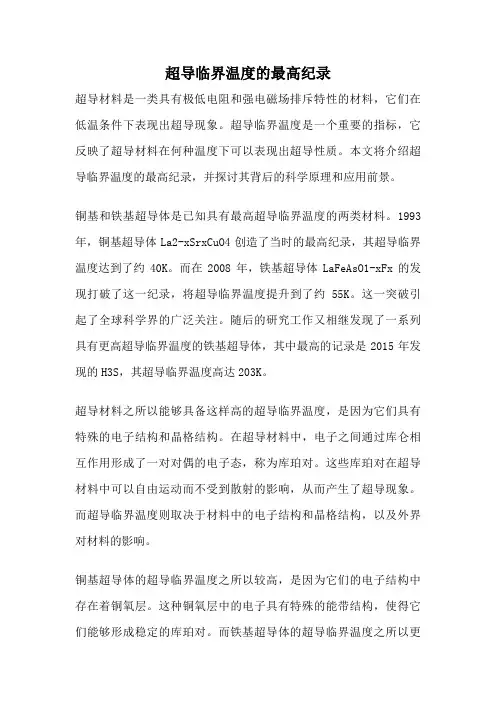
在SrTiO3衬底上成功生长出了FeSe薄膜,并在单层FeSe薄膜中发现可能存在接近液氮温度(77K)的超导转变迹象。这项工作,一方面可能打破铁基超导体最高超导温度55K的纪录。另一方面,因为该超导温度远高于块材FeSe常压下的超导转变温度~8K和高压下能达到的Tc~36.7K,这一结果相当地出人意料。到底是什么原因使得SrTiO3衬底上生长的单层FeSe薄膜显示出如此奇异的超导特性?这一问题的研究,对理解铁基超导体的超导机理,以及对研究如何提高材料的超导转变温度,都有着重要的意义。 单层FeSe薄膜的电子结构和已有的其它铁基超导体显著不同,具有非常简单的费米面(图1)。在布里渊区中心Γ点没有任何能带穿越费米能,只在布里渊区的角上M点,存在电子型的费米面(图2)。 其次,在低温下观察到M点附近费米面上超导能隙的打开。通过测量能隙随温度的变化,发现在55K左右能隙关闭,表明该样品的超导转变温度在55K附近(图3)。对超导能隙随动量变化关系的测量,表明能隙基本为各向同性(~15 meV)(图4)。由于这是一个理想的二维体系,由此可以直接判定该体系中没有能隙节点的存在。 单层FeSe具有如此简单的费米面,却同时具有如此高的超导温度,这对理解铁基超导体的超导机理提供了重要的信息。一方面,在这种理想的二维体系中观察到超导,说明三维的层间耦合对铁基高温超导电性的产生没有明显作用。另一方面,在已有的几类铁基超导体中,布里渊区中心Γ点附近普遍存在几个空穴型的能带和费米面,而且这些费米面被认为和超导电性的产生密切相关。结合之前对AxFe2-ySe2超导体的研究,单层FeSe的结果进一步表明,Γ点附近的空穴型费米面的存在对铁基超导体的超导电性的产生不一定是必要条件,而M点附近的电子型费米面则非常重要。这些信息一方面抓住了铁基超导产生的关键因素,另一方面有利于简化理论上的分析和处理。
图1. 单层FeSe薄膜的费米面(左上). 作为比较,图中也显示了(Ba,K)Fe2As2超导体(左下), AxFe2-ySe2
赵忠贤:探寻超导世界方案,带领团队很快将铁基超导体的临界温度提高到50K以上,创造了55K的纪录并保持至今,为确认铁基超导体为第二个高温超导家族提供了重要依据,实现了高温超导研究领域的第二次突破。
在这期间,他以67岁的年纪3次带领年轻人几乎通宵工作,完成了初期最关键的3篇论文。
赵忠贤的铁基超导研究得到了国内外的高度评价。
美国《科学》杂志3次报道赵忠贤小组的工作,其中在题为《新超导体将中国物理学家推向最前沿》的一篇文章中对于赵忠贤小组的贡献予以充分的肯定。
赵忠贤小组的成果作为“40K以上铁基高温超导体的发现及若干基本物理性质研究”的重要部分,荣获2013年度国家自然科学奖一等奖。
● 一生只做一件事“现在社会上各种诱惑很多,好像很多选择都比做科研赚钱,但如果选择了科研这条道路,不妨安下心来,坚持一下,我相信你们坚持十年一定会有重大突破。
”赵忠贤人生中最“郁闷”的时期是20世纪80年代。
国际物理学界在探索高温超导体的研究上遇到了瓶颈,相关研究跌入低谷。
国内的研究也受了影响,很多团队解散。
赵忠贤的研究完全停滞,这期间他不得不赴美一年帮着别人做研究,但最终他发现那不是自己喜欢的高温超导方向,于是迅速决定回国。
回国以后,他又不得不面对窘境——没有设备、没有团队、没有经费。
“热的时候坚持,冷的时候也坚持。
”赵忠贤带领超导团队坚守这块阵地,持之以恒地进行实验。
经费有限,他曾与同事自己动手绕制烧结炉,也曾将趁着“大减价”时淘换下来的“土炮”当作“重型武器”使用。
1986年底到1987年初,赵忠贤和同事们夜以继日地奋战在实验室中。
饿了,就煮面条;累了,轮流在椅子上打个盹。
在最困难的时候,他们充满信心,相互鼓励:“别看现在这个样品不超导,新的超导体很可能就诞生在下一个样品中。
”最终赵忠贤等到了。
中科院超导国家重点实验室研究员孙力玲与赵忠贤共事多年,她在接受采访时说,赵老师给我印象最深的就是他对科研方向的坚持,他真的做到了扎下根,决定一个方向然后就全力以赴。
S 4Symmetric Microscopic Model for Iron-Based SuperconductorsJiangping Hu 1,2and Ningning Hao 1,21Beijing National Laboratory for Condensed Matter Physics,Institute of Physics,Chinese Academy of Sciences,Beijing 100080,China2Department of Physics,Purdue University,West Lafayette,Indiana 47907,USA(Received 8March 2012;published 30May 2012)Although iron-based superconductors are multiorbital systems with complicated band structures,we demonstrate that the low-energy physics which is responsible for their high-T c superconductivity is essentially governed by an effective two-orbital Hamiltonian near half filling.This underlying electronic structure is protected by the S 4symmetry.With repulsive or strong next-nearest-neighbor antiferromagnetic exchange interactions,the model results in a robust A 1g s -wave pairing which can be mapped exactly to the d -wave pairing observed in cuprates.The classification of the super-conducting (SC)states according to the S 4symmetry leads to a natural prediction of the existence of two different phases,named the A and B phases.In the B phase,the superconducting order has an overall sign change along the c axis between the top and bottom As (or Se)planes in a single Fe-As (or Fe-Se)trilayer structure,the common building block of iron-based superconductors.The sign change is analogous to the sign change in the d -wave superconducting state of cuprates upon 90 rotation.Our derivation provides a unified understanding of iron pnictides and iron chalcogenides,and suggests that cuprates and iron-based superconductors share an identical high-T c superconducting mechanism.DOI:10.1103/PhysRevX.2.021009Subject Areas:Condensed Matter Physics,Strongly Correlated Materials,SuperconductivityI.INTRODUCTIONSince the discovery of iron-based superconductors [1–4],there has been considerable controversy over the choice of the appropriate microscopic Hamiltonian [5,6].The major reason behind such a controversy is the com-plicated multiple-d -orbital electronic structure of the materials.Although the electronic structure has been mod-eled by using different numbers of orbitals,ranging from a minimum of two [7],to three orbitals [8],and to all five d orbitals [9,10],a general perception has been that any microscopic model composed of fewer than all five d orbitals and ten bands is insufficient [6].Such a perception has blocked the path to understanding the superconducting mechanism because of the difficulty in identifying the key physics responsible for the high T c .Realistically,in a model with five orbitals,it is very difficult for any theo-retical calculation to make meaningful predictions in a controllable manner.Iron-based superconductors include two families:iron pnictides [1–3]and iron chalcogenides [4].The families share many intriguing common properties.They both have the highest T c s around 50K [2,5,11–13].The supercon-ducting gaps are close to being isotropic around Fermisurfaces [14–19],and the ratio between the gap and T c ,2Á=T c ,is much larger than the Bardeen-Cooper-Schrieffer ratio,3.52,in both families.However,the electronic struc-tures in the two families,in particular,the Fermi surface topologies,are quite different in the materials that reach high T c .The hole pockets are absent in iron chalcogenides but present in iron pnictides [14,17–19].The presence of the hole pockets has been necessary for superconductivity in the majority of studies and models which strongly depend on the properties of Fermi surfaces.Therefore,the absence of the hole pockets in iron chalcogenides has led to an intense debate over whether both families belong to the same category and share a common superconducting mechanism.Without a clear microscopic picture of the underlying electronic structure,such a debate cannot be settled.When they are observed by angle-resolved photoemis-sion microscopy (ARPES),a very intriguing property noted in the SC states of iron pnictides is that the SC gaps on different Fermi surfaces are nearly proportional to a simple form factor cos k x cos k y in the reciprocal space.This form factor has been observed in two fam-ilies of iron pnictides:the 122family (such as Ba 1Àx K x Fe 2As 2)[14,15,20,21]and the 111family (such as NaFe 1Àx Co x As )[22,23].Just like the d -wave form factor (cos k x Àcos k y )in cuprates,such a form factor indicates that the pairing between two next-nearest-neighbor iron sites in real space dominates.In contrast,in a multiorbital model,many theoreticalPublished by the American Physical Society under the terms of the Creative Commons Attribution 3.0License .Further distri-bution of this work must maintain attribution to the author(s)and the published article’s title,journal citation,andDOI.Selected for a Viewpoint in Physics PHYSICAL REVIEW X 2,021009(2012)calculations based on weak-coupling approaches have shown that the gap functions are very sensitive to de-tailed band structures and vary significantly when the doping changes[6,24–28].The robustness of the form factor has therefore been argued to favor strong-coupling approaches,which emphasize electron-electron correla-tion or the effective next-nearest-neighbor(NNN)anti-ferromagnetic(AF)exchange coupling J2[29–35]as a primary source of the pairing force.However,realisti-cally,it is very difficult to imagine that such a local exchange interaction remains identical between all d-orbital electrons if a multiple-d-orbital model is considered.In this paper,we demonstrate that the underlying electronic structure in iron-based superconductors,the low-energy physics responsible for superconductivity,is essentially governed by a two-orbital model obeying the S4 symmetry.The two-orbital model includes two nearly degenerate single-orbital parts that can be mapped to each other under the S4transformation.This electronic structure stems from the fact that the dynamics of the d xz and d yz orbitals are divided into two groups that are sepa-rately coupled to the top and bottom As(Se)planes in a single Fe-(As)Se trilayer structure.[Throughout the paper, Fe-(As)Se means either the Fe-As or Fe-Se trilayer struc-ture,the common building block of iron-based supercon-ductors.Similarly,As(Se)means either As or Se.]The twogroups can thus be treated as an S4isospin.The dressing of other orbitals in the d xz and d yz orbitals cannot alter the characteristics of the symmetry.The underlying electronic structure becomes transparent after one performs a gauge mapping in thefive-orbital model[10].The gauge mapping also reveals the equiva-lence between the A1g s-wave pairing and the d-wave pairing.After the gauge mapping,the band structure for each S4isospin component is characterized by Fermi sur-faces located around the anti-d-wave nodal points in the Brillouin zone,corresponding to the sublattice periodicity of the bipartite iron square lattice,as shown in Fig.1(a).In the presence of an AF exchange coupling J2or an effective on-site Hubbard interaction,the d-wave pairing defined in the sublattices can be argued to be favored,just like the case in cuprates.The d-wave pairing symmetry maps reversely to an A1g s-wave pairing in the original gauge setting.These results provide a unified microscopic understanding of iron pnictides and iron chalcogenides and explain why an s-wave SC state without the sign change on Fermi surfaces in iron chalcogenides driven by repulsive interaction can be so robust.Even more intriguing,since the different gauge settings do not alter any physical measurements,the results suggest that,in the A1g s-wave state,for each S4isospin component,there is a hidden sign change between the top As(Se)and the bottom As(Se)planes along the c axis. The S4symmetry adds a new symmetry classification to the SC states.For example,even in the A1g s-wave pairing state,there are the two phases,A and B,with respect to the S4symmetry.In the A phase,the relative SC phase between the two S4isospin components is zero,while,in the B phase,the relative SC phase is .Therefore,there is an overall phase shift between the top As(Se)and the bottom As(Se)planes in the B phase along the c axis.Such a sign change should be detectable experimentally.This property makes iron-based superconductors useful in many SC de-vice applications.An experimental setup,similar to those for determining the d-wave pairing in cuprates[36–38],is proposed to detect the phase shift.The detection of the sign change will strongly support the premise that cuprates and iron-based superconductors share an identical microscopic superconducting mechanism and will establish that repulsive interactions are responsible for super-conductivity.The paper is organized in the following way.In Sec.II,we perform a gauge mapping and discuss the emergence of the underlying electronic structure.In Sec.III,we show that the underlying electronic structure can be constructed by a two-orbital model obeying the S4 symmetry and discuss many general properties of the model.In Sec.IV,we discuss the classification of the SC states under the S4symmetry and propose a measure-ment to detect the phase shift along the c axis between the top and bottom As(Se)planes.In Sec.V,we discuss the analogy between iron-based superconductors and cuprates.xFIG.1.(a)The square lattice structure of a single iron layer: One cell includes two Fe ions shown as differentlyfilled black balls forming two sublattices.We use x-y coordinates to mark the original tetragonal lattices and x0-y0to mark the sublattice direction.(b)The gauge transformation is illustrated.The balls with red circles are affected by the gauge transformation.(c) and(d)The mapping from the s-wave to the d-wave pairing symmetry by the gauge transformation.JIANGPING HU AND NINGNING HAO PHYS.REV.X2,021009(2012)II.GAUGE MAPPING AND THE EQUIV ALENCE OF s-WAVE AND d-WAVE PAIRINGA.Gauge mappingWe start by asking whether there is an unidentified important electronic structure in iron-based superconduc-tors in a different gauge setting.We give a translationally invariant Hamiltonian that describes the electronic band structure of an Fe square lattice,^H 0¼Xij; ;t ij; ^fþi ; ^f j ; ;(1)where i,j label Fe sites; , label orbitals;and labels spin.We consider the following gauge transformation.As shown in Figs.1(a)and1(b),we group four neighboring iron sites to form a super site,and we mark half of the super sites in red.The gauge transformation,^U,adds a minus sign to all Fermionic operators^f i ; at every site i marked in red.After the transformation,the Hamiltonian becomes^H0¼^Uþ^H0^U:(2) The gauge-mapping operator^U is a unitary operator so the eigenvalues of^H0are not changed after the gauge trans-formation.It is also important to notice that the mapping does not change any standard interaction terms,such as conven-tional electron-electron interactions and spin-spin exchange ly,for a general Hamiltonian including interaction terms^H I,under the mapping,we obtain^H¼^Hþ^H I!^H0¼^Uþ^H^U¼^H00þ^H I:(3) It is also easy to see that every unit cell of the lattice in the new gauge setting includes four iron sites.The original translational invariance of an Fe-As(Se)layer has two Fe sites per unit cell.As we will show in the following section, the doubling of the unit cell matches the true hidden unit cell in the electronic structure when the orbital degree of freedom is considered.This is the fundamental reason why the new gauge reveals the underlying electronic structure.B.Equivalence of s-wave and d-wave pairing The gauge mapping has another important property.As shown in Figs.1(c)and1(d),this transformation maps the A1g s-wave cosðk xÞcosðk yÞpairing symmetry in the origi-nal Fe lattice to a familiar d-wave cos k0xÀcos k0y pairingsymmetry defined in the two sublattices,where(k x,k y)and (k0x,k0y)label momentum in Brillouin zones of the original lattice and sublattice,respectively.A similar mapping has been discussed in the study of a two-orbital iron ladder model[35,39]to address the equivalence of s-wave and d-wave pairing symmetry in one dimension.In an earlier paper[32],one of us and his collaborator suggested a phenomenological necessity for achieving high T c and selecting pairing symmetries:When the pair-ing is driven by a local AF exchange coupling,the pairing form factor has to match the Fermi surface topology in the reciprocal space.If this rule is valid and the iron-based superconductors are in the A1g s-wave state,we expect that the Fermi surfaces after the gauge mapping should be located in the d-wave antinodal points in the sublattice Brillouin zone.This is indeed the case,as we will show in the following sections.C.Band structures after gauge mapping Various tight-binding models have been proposed to represent the band structure of^H0.In Fig.2,we plot the band structure of^H0and the corresponding^H00for twoFIG.2.Three-orbital[30]andfive-orbital[10]models:(a),(e)The Fermi surfaces;(b),(f)the band dispersion along the high-symmetry lines;(c),(g)the Fermi surfaces after the gauge transformation;(d),(h)the band dispersions along the high-symmetry lines after the gauge transformation.The hopping parameters can be found in the two references.The y axis for(b),(d),(f),(h)is in units of E(ev).S4SYMMETRIC MICROSCOPIC MODEL FOR IRON-...PHYS.REV.X2,021009(2012)different models:a maximumfive-orbital model for iron pnictides[10],and a three-orbital model constructed for electron-overdoped iron chalcogenides[30].As shown in Fig.2,although there are subtle differences among the band structures of H00,striking common features are revealed for both models.First,exactly as expected,all Fermi surfaces after the gauge mapping are relocated around X0,the antinodal points in a standard d-wave super-conducting state in the sublattice Brillouin zone.This is remarkable because a robust d-wave superconducting state can be argued to be favored in such a Fermi surface topology in the presence of repulsive interaction or nearest-neighbor(NN)AF coupling in the sublattice [32,40].If we reversely map to the original gauge,the original Hamiltonian must have a robust s-wave pairing symmetry.Therefore,an equivalence between the A1g s-wave pairing and the d-wave pairing is clearly esta-blished by the gauge mapping.Second,the bands previously located at different places on the Fermi surface are magically linked in the new gaugesetting.In particular,the two bands that contribute to electron pockets are nearly degenerate and in thefive-orbital model,the bands that contribute to hole pockets are,remarkably,connected to them.Together with the fact that the unit cell has four iron sites in the new gauge setting,these unexpected connections lead us to believe that,in the original gauge,there should be just two orbitals that form bands that make connections from lower-energy bands to higher-energy ones and determine Fermi surfaces. Moreover,the two orbitals should form two groups which provide two nearly degenerate band structures.Finally, since the mapping does not change electron density, Fig.2reveals that the doping level in each structure should be close to halffilling.In summary,the gauge mapping reveals that the low-energy physics is controlled by a two-orbital model that produces two nearly degenerate bands.III.THE CONSTRUCTION OF A TWO-ORBITAL MODEL WITH THE S4SYMMETRY Having made the above observations,we move to con-struct an effective two-orbital model to capture the under-lying electronic structure revealed by the gauge mapping.A.Physical pictureOur construction is guided by the following several facts.First,the d orbitals that form the bands near the Fermi surfaces are strongly hybridized with the p orbitals of As(Se).Since the d x0z and d y0z have the largest overlapwith the p x0and p y0orbitals,it is natural for us to use d x0z and d y0z to construct the model.Second,in the previousconstruction of a two-orbital model,the C4v symmetry was used[7].The C4v symmetry is not a correct symmetry, however,if the hopping parameters are generated through the p orbitals of As(Se).Considering the As(Se)environ-ment,a correct symmetry for the d orbitals at the iron sites is the S4symmetry group.Third,there are two As(Se) planes which are separated in space along the c axis. Since there is little coupling between the p orbitals of the two planes,and the hoppings through the p orbitals are expected to dominate over the direct exchange hoppings between the d orbitals themselves,the two-orbital model could essentially be decoupled into two nearly degenerate one-orbital st,the model should have a transla-tional invariance with respect to the As(Se)plane. Given the above guidelines,it is very natural for us to divide the two d orbitals into two groups,as shown in Fig.3.One group includes the d x0z in the A sublattice and the d y0z in the B sublattice,and the other includes the d x0z in the B sublattice and the d y0z in the A sublattice,where A and B label the two sublattices of the iron square lattice,as shown in Fig.1(a).Thefirst group strongly couples to the p orbitals in the upper As(Se)layer,and the second group couples to those in the bottom As(Se)layer.We denote ^c i and^d i as Fermionic operators for the two groups, respectively,at each iron site.B.S4symmetry and the two-orbital model Without turning on couplings between the two groups,we seek a general tight-binding model to describe the band structure based on the S4symmetry.The S4transformation maps^c i to^d i .If we define the corresponding operators in the momentum space as^c k and^d k ,the S4transformation takes^c k^dk!!À^d k0þQ^c k0þQ!;(4) where k0¼ðk y;Àk xÞand Q¼ð ; Þfor given k¼ðk x;k yÞ. FIG.3.A sketch of the d x0z and d y0z orbitals,their orientations, and their coupling into the two As(Se)layers.The hopping parameters are indicated:The nearest-neighbor hopping is marked by t1x and t1y;the next-nearest-neighbor hoppings are t2and t02due to the broken symmetry along two different diagonal directions;and the third NN hopping is marked by t3x and t3y.The coupling between the two layers is marked by the nearest-neighbor hopping t c.JIANGPING HU AND NINGNING HAO PHYS.REV.X2,021009(2012)Now,we consider a tight-binding model for thefirst group.Here we limit the hopping parameters up to the third NN(TNN).As illustrated in Fig.3,the tight-binding model can be approximated by including NN hoppings(t1x,t1y),NNN hoppings(t2,t02),and TNN hoppings(t3x,t3y).The longer-range hoppings can be included if needed.For convenience,we can define t1s¼ðt1xþt1yÞ=2,t1d¼ðt1xÀt1yÞ=2,t2s¼ðt2þt02Þ=2and t2d¼ðt2Àt02Þ=2,t3s¼ðt3xþt3yÞ=2,and t3d¼ðt3xÀt3yÞ=2,where the labels s and d indicate hoppings of the s-wave type(where the hopping parameter is sym-metric under the90 -degree rotation)and d-wave type (where the hopping parameter changes sign under the 90 -degree rotation),respectively.A general tight-binding model can be written as^H0;one ¼k;2½t1sðcos k xþcos k yÞÀ2þt1dðcos k xÀcos k yÞ ^cþk ^c k þ4½t2s cos k x cos k y^cþk ^c kþt2d sin k x sin k y^cþk ^c kþQ þ2½t3sðcos2k xþcos2k yÞþt3dðcos2k xÀcos2k yÞ ^cþk ^c k þ...:(5)We can apply the S4transformation to^H0;one to obtain the tight-binding model for the second group.The transformation invariance requires t1s,t2d,and t3d to change signs.Therefore,the two-orbital model is described by^H0;two ¼Xk½4t2s cos k x cos k yÀ ð^cþk ^c k þ^dþk ^d k Þþ2t1sðcos k xþcos k yÞð^cþk ^c k À^dþk ^d k Þþ2t1dðcos k xÀcos k yÞð^cþk ^c k þ^dþk ^d k Þþ4t2d sin k x sin k yð^cþk ^c kþQ À^dþk ^d kþQ Þþ2t3sðcos2k xþcos2k yÞð^cþk ^c k þ^dþk ^d k Þþ2t3dðcos2k xÀcos2k yÞð^cþk ^c k À^dþk ^d k Þþ...:(6)Now we can turn on the couplings between the two groups. It is straightforward to show that the leading order of the couplings that satisfies the S4symmetry is given by^H 0;c ¼Xk2t cðcos k xþcos k yÞð^cþk ^d k þH:c:Þ:(7)Combining^H0;two and^H0;c,we obtain an effective S4-symmetric two-orbital model whose band structure is described by^H0;eff¼^H0;twoþ^H0;c:(8)The^c and^d Fermionic operators can be viewed as two isospin components of the S4symmetry.Let us assume t c to be small and check whether^H0;eff can capture the electronic structure at low energy.Ignoring t c,^H0;eff provides the following energy dispersions for the two orbitals:E eƼ kÆ2t3dðcos2k xÀcos2k yÞþ4ffiffiffiffiffiffiffiffiffiffiffiffiffiffiffiffiffiffiffiffiffiffiffiffiffiffiffiffiffiffiffiffiffiffiffiffiffiffiffiffiffiffiffiffiffiffiffiffiffiffiffiffiffiffiffiffiffiffiffiffiffiffiffiffiffiffiffiffiffiffiffiffiffiffiffiffiffiffiffiffiffiffiffiffiffiffiffiffiffiffiffiffiffiffiffiffiffiffiffiffiffiffiffiffiffiffiffiffiffiffiffiffiffiffiffiffiffiffiffiffiffiffiffit22d sin2x sin2yþt1sðcos k xþcos k yÞÆt1dðcos k xÀcos k yÞ 2s;(9)E hƼ kÆ2t3dðcos2k xÀcos2k yÞÀ4ffiffiffiffiffiffiffiffiffiffiffiffiffiffiffiffiffiffiffiffiffiffiffiffiffiffiffiffiffiffiffiffiffiffiffiffiffiffiffiffiffiffiffiffiffiffiffiffiffiffiffiffiffiffiffiffiffiffiffiffiffiffiffiffiffiffiffiffiffiffiffiffiffiffiffiffiffiffiffiffiffiffiffiffiffiffiffiffiffiffiffiffiffiffiffiffiffiffiffiffiffiffiffiffiffiffiffiffiffiffiffiffiffiffiffiffiffiffiffiffiffiffiffit22d sin2x sin2yþt1sðcos k xþcos k yÞÆt1dðcos k xÀcos k yÞ22s;(10)where k¼4t2s cos k x cos k yþ2t3sðcos2k xþcos2k yÞÀ . Wefind that E eÆcan capture the electron pockets at M points and that E hÆcan capture the hole pockets atÀpoints.Based on the previous physical picture,t1s,t2s, and t2d should be the largest parameters because they are generated through the p orbitals.In Fig.4,we show that, by just keeping these three parameters,the model is al-ready good enough to capture the main characteristics of the bands contributing to Fermi surfaces in thefive-orbital model.After one performs the same gauge mapping,this Hamiltonian,as expected,provides pockets located at X0, as shown in Fig.4.C.General properties of the modelThe above model is capable of quantitatively describing the experimental results measured by ARPES[14,20,41–44]. Although the hopping parameters are dominated by t1s,t2d, and t2s,other parameters cannot be ignored.For example,at the same M points,there is energy splitting between two components,which indicates the existence of a sizable t1d.To match the detailed dispersion of the bands,the TNN hoppings have to be included.The existence of the TNN hoppings may also provide a microscopic justi-fication for the presence of the significant TNN AF exchangeS4SYMMETRIC MICROSCOPIC MODEL FOR IRON-...PHYS.REV.X2,021009(2012)coupling J 3,measured by neutron scattering in iron chalco-genides [32,45,46].While the detailed quantitative results for different fam-ilies of iron-based superconductors will be presented else-where [41],we now plot a typical case for iron pnictides with parameters t 1s ¼0:4,t 1d ¼À0:03,t 2s ¼0:3,t 2d ¼0:6,t 3s ¼0:05,t 3d ¼À0:05,and ¼À0:3in Figs.5(a)–5(d).In Figs.5(a)and 5(b),the coupling t c ¼0.In Figs.5(c)and 5(d),t c ¼0:02.It is clear that the degeneracy at the hole pockets along the À-X direction is lifted by t c .The Fermisurfaces in Fig.5are very close to those in the five-orbital model [10].This result is consistent with our assumption that t c is effectively small.The model has several interesting properties.First,it unifies the iron pnictides and iron chalcogenides.When other parameters are fixed,reducing t 2s or increasing t 1s can flatten the dispersion along the À-M direction of E h Æand cause the hole pocket to vanish completely.Therefore,the model can describe both iron pnictides and electron-overdoped iron chalcogenides by varying t 2s or t 1s .Second,carefully examining the hopping parameters,we also find that the NNN hopping for each S 4isospin essentially has a d -wave symmetry,namely,j t 2d j >t 2s .Since the hole pockets can be suppressed by reducing the value of t 2s ,this d -wave hopping symmetry is expected to be stronger in iron chalcogenides than in iron pnictides.Third,it is interesting to point out that we can make an exact analogy between the S 4transformation on its two isospin components and the time-reversal symmetry transformation on a real 1=2-spin because S 24¼À1.This analogy suggests that,in this S 4-symmetric model,the degeneracy at high-symmetry points in the Brillouin zone is of the Kramers type.Finally,in this model,if the orbital degree of freedom is included,the true unit cell for each isospin component includes four iron atoms.The gauge mapping in the pre-vious section takes exactly a unit cell with four iron sites.Such a match is the essential reason why the low-energy physics becomes transparent after the gauge mapping.D.The two-orbital model with interactions By projecting all interactions into these two effective orbital models,a general effective model that describesFIG.5.Typical Fermi surfaces (a)and band dispersions (b)resulting from Eq.(10),with t c ¼0and parameters t 1s ¼0:4,t 1d ¼À0:03,t 2s ¼0:3,t 2d ¼0:6,t 3s ¼0:05,t 3d ¼À0:05,and ¼À0:3.(c),(d)show the corresponding results when t c ¼0:02is used in Eq.(7)with the same parameter settings.The y axis for (b),(d)is in units of E(ev).FIG.4.The Fermi surfaces of each component when only parameters t 1s ,t 2d ,and t 2s are considered.The layout for (a)–(h)exactly follows that of Fig.2.The parameters are t 1¼0:24,t 2¼0:52,and ¼À0:273.The only difference in parameters between (a)and(e)is that t 02¼À0:1in (a)and t 02¼À0:2in (e).The y axis for (b),(d),(f),(h)is in units of E(ev).JIANGPING HU AND NINGNING HAOPHYS.REV .X 2,021009(2012)iron-based superconductors obeying the S 4symmetry can be written as^H eff ¼^H 0;eff þU Xi; ¼1;2^n i; "^n i; #þU 0X i^n i;1^n i;2þJ 0HXi^Si;1Á^S i;2;(11)where ¼1;2labels the S 4isospin,U describes theeffective Hubbard repulsion interaction within each com-ponent,U 0describes the one between them,and J 0H de-scribes the effective Hund’s coupling.Since the two components couple weakly,we may expect that U domi-nates over U 0and J 0H .Then,in the first-order approxima-tion,the model could become a single-band Hubbard model near half filling.A similar t -J model can also be discussed within the same context as cuprates [47,48].It is clear that the model naturally provides an explanation for the stable NNN AF exchange couplings J 2observed by neutron scattering [45,46,49]and the dominating role of J 2in both magnetism and superconductivity [32].E.Reduction of the symmetry from D 2d to S 4The true lattice symmetry in an Fe-As(Se)trilayer is the D 2d point group,where S 4is a subgroup of the D 2d .In the D 2d group,besides the S 4invariance,the reflection opera-tor v with respect to the x 0-z plane is also invariant.The reflection imposes an additional requirement,^ck ^d k !!^c k 00þQ À^d k 00þQ !;(12)where k 00¼ðk y ;k x Þ.It is easy to see that if we imposethe D 2d symmetry,the reflection v invariance requires t 1s ¼0.However,without such a reflection invariance,t 1s is allowed,which is the case when only the S 4symmetry remains.The existence of t 1s suggests that v symmetry must be broken in an effective model.However,since v symmetry appears to be present,it is natural to ask what mechanism can break v .While a detailed study of this symmetry breaking is in preparation [50],we give a brief analysis.Among the five d orbitals,d xy ,d x 2Ày 2,and d z 2belong to one-dimensional representations of the D 2d group.In fact,for these three orbitals,the D 2d group is equivalent to the C 4v group.In other words,the As(Se)separation along the c axis has no effect on the symmetry of the kinematics of the three orbitals if the couplings to the other two orbitals,d xz and d yz ,are not included.Therefore,for these three orbitals,the unit cell is not doubled by As(Se)atoms,and the band structure is intrinsically one iron per unit cell even if the hoppings generated through p orbitals of As(Se)are important.However,for the d xz and d yz orbitals,if the hoppings through p orbitals of As(Se)are dominant,the unit cell is doubled by As(Se)atoms and the band structure is intrinsically folded.From Eq.(12),after theS 4symmetry is maintained,the v -symmetry operations simply map the reduced Brillouin zone to the folded part in the original Brillouin zone.If the couplings between the above two groups of orbitals are turned on,the effective two orbitals that describe the low-energy physics near Fermi surfaces are not pure d xz ,d yz orbitals any more.In particular,they are heavily dressed by d xy orbitals,as shown in ARPES [51–54].Therefore,the effective two orbitals can keep only the S 4symmetry,and the v sym-metry has to be broken.Another possibility for generation of the t 1s hopping may stem from the following virtual hopping processes:One electron first hops from the p x to the d xz ,and then,an electron in the p y at the same As(Se)site can hop to the p x .Finally,an electron in the d yz orbital hops to the p y .In such a process,the reflection symmetry is broken due to the existence of the hopping between the p x and p y orbitals at the same As(Se)site when the two orbitals host a total of 3electrons,which is possible if the on-site Hubbard interac-tion U in p orbitals is sufficiently large such that the degeneracy of p x and p y is broken,a result of the standard Jahn–Teller effect.F.The coupling between two S 4isospinsand S 4symmetry breakingThe couplings between the two isospins can either keep the S 4symmetry or break it.Without breaking the transla-tional symmetry,the coupling between two orbitals can be written as^H c ¼X k;f ðk Þ^G ðk ÞþXk;"f " ðk Þ^G "ðk Þ;(13)where ^G ðk Þand ^G " ðk Þare operators constructed accord-ing to the S 4one-dimensional representations,as follows:^G 1ðk Þ¼Xc þk ^d k þc þk þQ ^d k þQ þH :c :;(14)^G 2ðk Þ¼Xc þk ^d k Àc þk þQ ^d k þQ þH :c :;(15)^G 3ðk Þ¼Xc þk ^d k þQ þc þk þQ ^d k þH :c :;(16)^G 4ðk Þ¼Xc þk ^d k þQ Àc þk þQ ^d k þH :c :;(17)^G "1ðk Þ¼Xi ðc þk ^d k þc þk þQ ^d k þQ ÀH :c :Þ;(18)^G "2ðk Þ¼Xi ðc þk ^d k Àc þk þQ ^d k þQ ÀH :c :Þ;(19)^G "3ðk Þ¼Xi ðc þk ^d k þQ þc þk þQ ^d k ÀH :c :Þ;(20)S 4SYMMETRIC MICROSCOPIC MODEL FOR IRON-...PHYS.REV .X 2,021009(2012)。
超导体分类超导体是一种具有零电阻和完全排斥外磁场的材料。
它们在科学研究和技术应用中具有广泛的用途。
根据不同的特性和应用,超导体可以分为不同的类型。
第一类超导体是最早被发现的超导体。
它们在低温下表现出完全的电阻消失,而且只在临界温度以下才能发生超导现象。
第一类超导体的关键特点是它们只能在非常低的温度下工作,通常在液氮温度以下。
这限制了它们的应用范围,但在某些特定领域仍然非常有用。
第二类超导体是一类相对较新的材料,也是目前应用最广泛的超导体。
与第一类超导体不同,第二类超导体可以在相对较高的温度下工作。
它们的临界温度通常在液氮温度以上,甚至有些可以在室温下工作。
这使得第二类超导体在实际应用中更加方便。
第二类超导体的特点是它们可以承受较强的磁场,并且具有较高的临界电流密度。
这使得它们在磁共振成像、能源传输和磁悬浮等领域具有广泛的应用。
此外,第二类超导体还可以用于制造超导磁体和超导电缆等设备,以提高能源传输效率和减少能量损耗。
除了第一类和第二类超导体,还有一些特殊类型的超导体。
例如,高温超导体是指临界温度高于液氮温度的超导体。
这些材料具有更高的临界温度,因此在实际应用中更具吸引力。
此外,铁基超导体是一类以铁元素为主要成分的超导体,具有独特的电子结构和超导性质。
超导体是一类具有特殊电导特性的材料。
根据不同的特性和应用,超导体可以分为第一类、第二类、高温超导体和铁基超导体等不同类型。
这些超导体在科学研究和技术应用中发挥着重要作用,具有广阔的发展前景。
随着对超导体的研究和应用的不断深入,相信超导技术将为人类带来更多的惊喜和突破。