
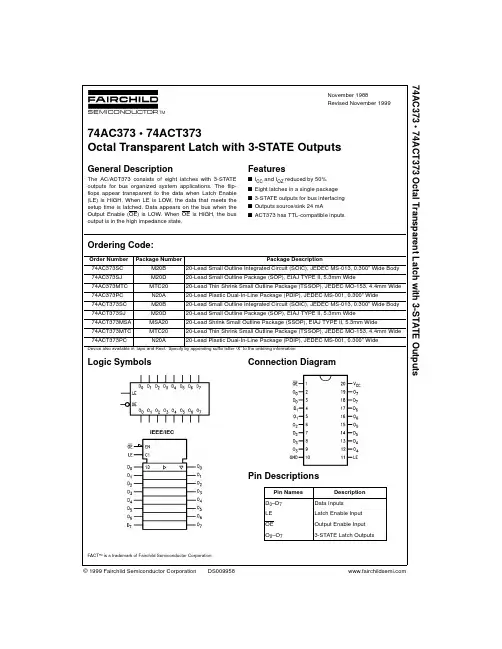
74ACT373SC中文资料
- 格式:pdf
- 大小:110.23 KB
- 文档页数:10
Rev.2.00 Mar 30, 2006 page 1 of 8
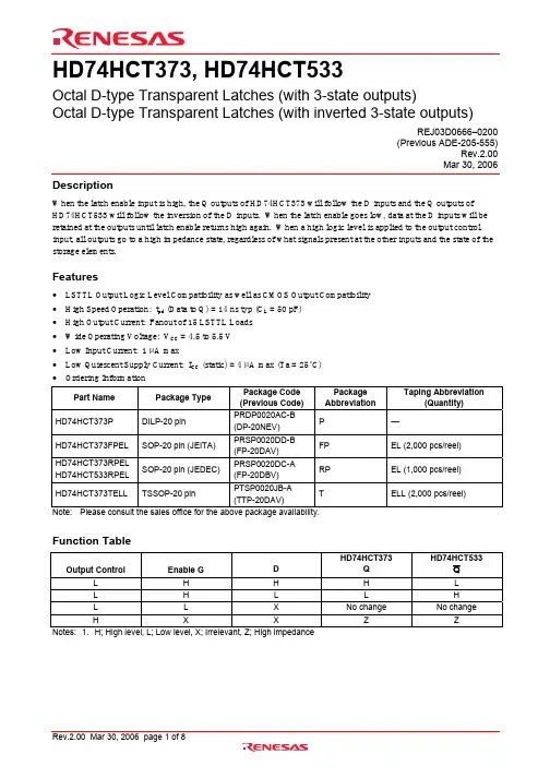
HD74HCT373, HD74HCT533
Octal D-type Transparent Latches (with 3-state outputs)
Octal D-type Transparent Latches (with inverted 3-state outputs)
REJ03D0666–0200
(Previous ADE-205-555) Rev.2.00
Mar 30, 2006
Description
When the latch enable input is high, the Q outputs of HD74HCT373 will follow the D inputs and the Q outputs of
HD74HCT533 will follow the inversion of the D inputs. When the latch enable goes low, data at the D inputs will be
retained at the outputs until latch enable returns high again. When a high logic level is applied to the output control
input, all outputs go to a high impedance state, regardless of what signals present at the other inputs and the state of the
storage elements.
Features
• LSTTL Output Logic Level Compatibility as well as CMOS Output Compatibility
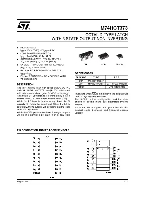
1/11August 2001sHIGH SPEED: tPD = 19ns (TYP.) at VCC = 4.5VsLOW POWER DISSIPATION:ICC = 4µA(MAX.) at TA=25°CsCOMPATIBLE WITH TTL OUTPUTS : VIH = 2V (MIN.) VIL = 0.8V (MAX)sSYMMETRICAL OUTPUT IMPEDANCE:|IOH| = IOL = 6mA (MIN)sBALANCED PROPAGATION DELAYS:tPLH ≅ tPHL sPIN AND FUNCTION COMPATIBLE WITH 74 SERIES 373
DESCRIPTIONThe M74HCT373 is an high speed CMOS OCTALLATCH WITH 3-STATE OUTPUTS fabricatedwith sub-micron silicon gate C2MOS technology.This 8-BIT D-Type latches is controlled by a latchenable input (LE) and output enable input (OE).While the LE input is held at a high level, the Qoutputs will follow the data input. When the LE istaken low, the Q outputs will be latched at the logiclevel of D input data. While the OE input is at low level, the eight outputswill be in a normal logic state (high or low logiclevel) and when OE is in high level the outputs willbe in a high impedance state.The 3-State output configuration and the widechoice of outline make bus organized systemsimple.All inputs are equipped with protection circuitsagainst static discharge and transient excessvoltage.M74HCT373

74系列芯片数据手册大全
74系列芯片数据手册大全
74系列集成电路名称与功能常用74系列标准数字电路的中文名称资料7400 TTL四2输入端四与非门
7401 TTL 集电极开路2输入端四与非门
7402 TTL 2输入端四或非门
7403 TTL 集电极开路2输入端四与非门
7404 TTL 六反相器
7405 TTL 集电极开路六反相器
7406 TTL 集电极开路六反相高压驱动器
7407 TTL 集电极开路六正相高压缓冲驱动器
7408 TTL 2输入端四与门
7409 TTL 集电极开路2输入端四与门
7410 TTL 3输入端3与非门
74107 TTL 带清除主从双J-K触发器
74109 TTL 带预置清除正触发双J-K触发器
7411 TTL 3输入端3与门
74112 TTL 带预置清除负触发双J-K触发器
7412 TTL 开路输出3输入端三与非门
74121 TTL 单稳态多谐振荡器
74122 TTL 可再触发单稳态多谐振荡器
74123 TTL 双可再触发单稳态多谐振荡器
74125 TTL 三态输出高有效四总线缓冲门
74126 TTL 三态输出低有效四总线缓冲门
7413 TTL 4输入端双与非施密特触发器
74132 TTL 2输入端四与非施密特触发器
74133 TTL 13输入端与非门
74136 TTL 四异或门
74138 TTL 3-8线译码器/复工器 74139 TTL 双2-4线译码器/复工器
7414 TTL 六反相施密特触发器
74145 TTL BCD—十进制译码/驱动器
7415 TTL 开路输出3输入端三与门
74150 TTL 16选1数据选择/多路开关
74151 TTL 8选1数据选择器
74153 TTL 双4选1数据选择器
74154 TTL 4线—16线译码器
74155 TTL 图腾柱输出译码器/分配器
74156 TTL 开路输出译码器/分配器
Original Creation Date: 11/18/96Last Update Date: 06/19/97Last Major Revision Date: 04/17/97CN74F373-X REV 1A0MICROCIRCUIT DATA SHEETOCTAL TRANSPARENT LATCH WITH TRI-STATE OUTPUTS General DescriptionThe F373 consists of eight latches with Tri-State outputs for bus organized systemapplications. The flip-flops appear transparent to the data when Latch Enable (LE) isHIGH. When LE is LOW, the data that meets the setup times are latched. Data appear onthe bus when the Output Enable (OE) is LOW. When OE is HIGH, the bus output is in thehigh impedance state. NS Part Numbers74F373DCIndustry Part Number74F373Prime DieM373ProcessingQuality Conformance InspectionSubgrp Description Temp ( C)o1Static tests at +252Static tests at +703Static tests at 04Dynamic tests at +255Dynamic tests at +706Dynamic tests at 07Functional tests at +258AFunctional tests at +708BFunctional tests at 09Switching tests at +2510Switching tests at +7011