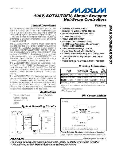
MAX4515EUK-T中文资料
- 格式:pdf
- 大小:391.59 KB
- 文档页数:8
_______________General DescriptionThe MAX4514/MAX4515 are single-pole/single-throw (SPST), CMOS, low-voltage, single-supply analog switches with very low switch on-resistance. The MAX4514 is normally open (NO). The MAX4515 is nor-mally closed (NC).These CMOS switches can operate continuously with a single supply between +2V and +12V. Each switch can handle rail-to-rail analog signals. The off-leakage cur-rent maximum is only 1nA at +25°C or 20nA at +85°C.All digital inputs have 0.8V to 2.4V logic thresholds,ensuring TTL/CMOS-logic compatibility when using a +5V supply.For pin-compatible parts for use with dual supplies, see the MAX4516/MAX4517.________________________ApplicationsBattery-Operated Equipment Audio and Video Signal Routing Low-Voltage Data-Acquisition Systems Communications Circuits PCMCIA Cards Cellular Phones Modems____________________________Featureso Available in SOT23-5 Package o +2V to +12V Single-Supply Operation o Guaranteed On-Resistance:20Ωwith +5V Supply 10Ωwith +12V Supplyo Guaranteed Low Off-Leakage Currents:1nA at +25°C 20nA at +85°C o Guaranteed Low On-Leakage Currents:2nA at +25°C 40nA at +85°C o Low Charge Injection: 10pCo Fast Switching Speed: t ON = 150ns, t OFF = 100ns o Break-Before-Make Operation: t ON > t OFF at +5V o TTL/CMOS-Logic Compatible with +5V SupplyMAX4514/MAX4515Low-Voltage, Low-On-Resistance,SPST, CMOS Analog Switches________________________________________________________________Maxim Integrated Products 1__________________________________________________________Pin Configurations19-1069; Rev 1; 5/05Ordering Information continued at end of data sheet.*Contact factory for dice specifications.For pricing, delivery, and ordering information,please contact Maxim/Dallas Direct!at 1-888-629-4642, or visit Maxim’s website at .M A X 4514/M A X 4515Low-Voltage, Low-On-Resistance,SPST, CMOS Analog SwitchesABSOLUTE MAXIMUM RATINGSELECTRICAL CHARACTERISTICS —+5V Supply(V+ = +4.5V to +5.5V, V INH = 2.4V, V INL = 0.8V, T A = T MIN to T MAX , unless otherwise noted. Typical values are at T A = +25°C.)Stresses beyond those listed under “Absolute Maximum Ratings” may cause permanent damage to the device. These are stress ratings only, and functional operation of the device at these or any other conditions beyond those indicated in the operational sections of the specifications is not implied. Exposure to absolute maximum rating conditions for extended periods may affect device reliability.Note 1:Voltages exceeding V+ or GND on any signal terminal are clamped by internal diodes. Limit forward-diode current tomaximum current rating.(Voltages referenced to GND.)V+..............................................................................-0.3V, +13V Voltage into Any Terminal (Note 1)...............-0.3V to (V+ + 0.3V)or ±20mA (whichever occurs first)Continuous Current into Any Terminal..............................±20mA Peak Current, NO_ or COM_(pulsed at 1ms,10% duty cycle)....................................±30mA ESD per Method 3015.7..................................................>2000V Continuous Power Dissipation (T A = +70°C)8-Pin Plastic DIP (derate 9.09mW/°C above +70°C)....727mW 8-Pin SO (derate 5.88mW/°C above +70°C).................471mW5-Pin SOT23-5 (derate 7.1mW/°C above +70°C).........571mW 8-Pin CERDIP (derate 8.00mW/°C above +70°C).........640mW Operating Temperature RangesMAX4514C_ _/MAX4515C_ _..............................0°C to +70°C MAX4514E_ _/MAX4515E_ _............................-40°C to +85°C MAX4514MJA/MAX4515MJA.........................-55°C to +125°C Storage Temperature Range.............................-65°C to +150°C Lead Temperature (soldering, 10s).................................+300°CMAX4514/MAX4515Low-Voltage, Low-On-Resistance,SPST, CMOS Analog Switches_______________________________________________________________________________________3ELECTRICAL CHARACTERISTICS —+5V Supply (continued)(V+ = +4.5V to +5.5V, V INH = 2.4V, V INL = 0.8V, T A = T MIN to T MAX , unless otherwise noted. Typical values are at T A = +25°C.)ELECTRICAL CHARACTERISTICS —+12V Supply(V+ = +11.4V to +12.6V, V INH = 5V, V INL = 0.8V, T A = T MIN to T MAX , unless otherwise noted. Typical values are at T A = +25°C.)300510023415ON-RESISTANCEvs. V COM OVER TEMPERATUREV COM (V)R O N (Ω)1520251001068102412ON-RESISTANCE vs. V COMV COM (V)RO N (Ω)1030-10-550064810212CHARGE INJECTION vs. V COMV COM (V)Q (p C )15102025__________________________________________Typical Operating Characteristics(V+ = +5V, GND = 0V, T A = +25°C, unless otherwise noted.)M A X 4514/M A X 4515Low-Voltage, Low-On-Resistance,SPST, CMOS Analog Switches 4_______________________________________________________________________________________ELECTRICAL CHARACTERISTICS —+3V Supply(V+ = +3V to +3.6V, T A = T MIN to T MAX , unless otherwise noted. Typical values are at T A = +25°C.)Note 3:Leakage parameters are 100% tested at maximum-rated hot operating temperature, and are guaranteed by correlation at +25°C.Note 4:Guaranteed, not production tested.Note 5:SOT packaged parts are 100% tested at +25°C. Limits at maximum and minimum rated temperature are guaranteed by design and correlation limits at +25°C.MAX4514/MAX4515Low-Voltage, Low-On-Resistance,SPST, CMOS Analog Switches51001010.10.00001-60406080100120-40-20020140ON/OFF-LEAKAGE vs. TEMPERATURETEMPERATURE (°C)O N /O F F L E A K A G E (n A )0.010.0010.00011000.0110100010,000100100,000TOTAL HARMONIC DISTORTIONvs. FREQUENCY0.1FREQUENCY (Hz)T H D (%)1100-10-20-30-50-40-1200.00011101000.0010.010.11000FREQUENCY RESPONSEFREQUENCY (MHz)L O S S (d B )P H A S E (D E G R E E S )-60-70-90-80-100-110605040301020-600-10-30-20-40-501601802000206040064810212t ON /t OFF vs. V SUPPLYV+ SUPPLY (V)t O N /t O F F (n s )10080120140____________________________Typical Operating Characteristics (continued)(V+ = +5V, GND = 0V, T A = +25°C, unless otherwise noted.)______________________________________________________________Pin DescriptionNote:NO, NC, and COM pins are identical and interchangeable. Any may be considered as an input or an output; signals passequally well in both directions.M A X 4514/M A X 4515Low-Voltage, Low-On-Resistance,SPST, CMOS Analog Switches 6_________________________________________________________________________________________________Applications InformationPower-Supply ConsiderationsThe MAX4514/MAX4515 construction is typical of most CMOS analog switches, except that they have only two supply pins: V+ and GND. V+ and GND drive the inter-nal CMOS switches and set their analog voltage limits.Reverse ESD-protection diodes are internally connect-ed between each analog-signal pin and both V+ and GND. One of these diodes conducts if any analog sig-nal exceeds V+ or GND.Virtually all the analog leakage current comes from the ESD diodes to V+ or GND. Although the ESD diodes on a given signal pin are identical and therefore fairly well balanced, they are reverse biased differently. Each is biased by either V+ or GND and the analog signal. This means their leakages will vary as the signal varies. The difference in the two diode leakages to the V+ and GND pins constitutes the analog-signal-path leakage current.All analog leakage current flows between each pin and one of the supply terminals, not to the other switch termi-nal. This is why both sides of a given switch can show leakage currents of the same or opposite polarity.There is no connection between the analog-signal paths and V+ or GND.V+ and G ND also power the internal logic and logic-level translators. The logic-level translators convert the logic levels to switched V+ and G ND signals to drive the analog signal gates.Logic-Level ThresholdsThe logic-level thresholds are CMOS/TTL compatible when V+ is +5V. As V+ is raised, the level threshold increases slightly. When V+ reaches +12V, the level threshold is about 3.0V—above the TTL guaranteed high-level minimum of 2.8V, but still compatible with CMOS outputs.Do not connect the MAX4514/MAX4515’s V+ to +3V and then connect the logic-level pins to logic-level signals that operate from +5V supply. Output levels can exceed +3V and violate the absolute maximum ratings, damaging the part and/or external circuits.High-Frequency PerformanceIn 50Ωsystems, signal response is reasonably flat up to 250MHz (see Typical Operating Characteristics ). Above 20MHz, the on response has several minor peaks that are highly layout dependent. The problem is not in turn-ing the switch on; it’s in turning it off. The off-state switch acts like a capacitor and passes higher frequencies with less attenuation. At 10MHz, off isolation is about -45dB in 50Ωsystems, decreasing (approximately 20dB per decade) as frequency increases. Higher circuit imped-ances also make off isolation decrease. Off isolation is about 3dB above that of a bare IC socket, and is due entirely to capacitive coupling.Figure 1. Charge Injection ______________________________________________Test Circuits/Timing DiagramsMAX4514/MAX4515Low-Voltage, Low-On-Resistance,SPST, CMOS Analog Switches_______________________________________________________________________________________7Figure 2. Switching Times_________________________________Test Circuits/Timing Diagrams (continued)Figure 3. Off-Isolation and On-Loss Figure 4. NO, NC, and COM CapacitanceMaxim cannot assume responsibility f or use of any circuitry other than circuitry entirely embodied in a Maxim product. No circuit patent licenses are implied. Maxim reserves the right to change the circuitry and specifications without notice at any time.8___________________Maxim Integrated Products, 120 San Gabriel Drive, Sunnyvale, CA 94086 (408) 737-7600©2005 Maxim Integrated ProductsPrinted USAis a registered trademark of Maxim Integrated Products, Inc.M A X 4514/M A X 4515Low-Voltage, Low-On-Resistance,SPST, CMOS Analog Switches _Ordering Information (continued)__________________________________________________Tape-and-Reel InformationWB 0K 0t+0.305 -0.102P 0 3.988 ±0.102P 010 40.005P 2 2.007t 0.254W8.001*Contact factory for dice specifications.**Contact factory for availability.___________________Chip TopographyTRANSISTOR COUNT: 19SUBSTRATE IS INTERNALLY CONNECTED TO V+0.031"(0.79mm)。